EP0668508B1 - Electric field sensor - Google Patents
Electric field sensor Download PDFInfo
- Publication number
- EP0668508B1 EP0668508B1 EP94919869A EP94919869A EP0668508B1 EP 0668508 B1 EP0668508 B1 EP 0668508B1 EP 94919869 A EP94919869 A EP 94919869A EP 94919869 A EP94919869 A EP 94919869A EP 0668508 B1 EP0668508 B1 EP 0668508B1
- Authority
- EP
- European Patent Office
- Prior art keywords
- electric field
- antenna elements
- substrate
- field sensor
- phase
- Prior art date
- Legal status (The legal status is an assumption and is not a legal conclusion. Google has not performed a legal analysis and makes no representation as to the accuracy of the status listed.)
- Expired - Lifetime
Links
Images


Classifications
-
- G—PHYSICS
- G01—MEASURING; TESTING
- G01R—MEASURING ELECTRIC VARIABLES; MEASURING MAGNETIC VARIABLES
- G01R15/00—Details of measuring arrangements of the types provided for in groups G01R17/00 - G01R29/00, G01R33/00 - G01R33/26 or G01R35/00
-
- G—PHYSICS
- G01—MEASURING; TESTING
- G01R—MEASURING ELECTRIC VARIABLES; MEASURING MAGNETIC VARIABLES
- G01R15/00—Details of measuring arrangements of the types provided for in groups G01R17/00 - G01R29/00, G01R33/00 - G01R33/26 or G01R35/00
- G01R15/14—Adaptations providing voltage or current isolation, e.g. for high-voltage or high-current networks
- G01R15/24—Adaptations providing voltage or current isolation, e.g. for high-voltage or high-current networks using light-modulating devices
- G01R15/241—Adaptations providing voltage or current isolation, e.g. for high-voltage or high-current networks using light-modulating devices using electro-optical modulators, e.g. electro-absorption
-
- G—PHYSICS
- G01—MEASURING; TESTING
- G01R—MEASURING ELECTRIC VARIABLES; MEASURING MAGNETIC VARIABLES
- G01R29/00—Arrangements for measuring or indicating electric quantities not covered by groups G01R19/00 - G01R27/00
- G01R29/08—Measuring electromagnetic field characteristics
- G01R29/0864—Measuring electromagnetic field characteristics characterised by constructional or functional features
- G01R29/0878—Sensors; antennas; probes; detectors
- G01R29/0885—Sensors; antennas; probes; detectors using optical probes, e.g. electro-optical, luminiscent, glow discharge, or optical interferometers
Definitions
- This invention relates to an electric field sensor for measuring an electric field intensity of an electromagnetic wave or the like.
- Fig. 1 shows a conventional electric field sensor.
- the electric field sensor comprises a sensor head 1 and an antenna 2 connected to the sensor head 1.
- the sensor head 1 has a substrate 3 and an optical modulator 4 attached to the substrate 3.
- the optical modulator 4 comprises an incident optical waveguide 5 formed on the substrate 3, two phase-shift optical waveguides 6 which are formed on the substrate 3 to be branched from the incident optical waveguide 5 and each of which has a variable refractive index varying in response to an electric field intensity applied thereto, an outgoing optical waveguide 7 formed on the substrate 3 to join the phase-shift optical waveguides 6, and two modulation electrodes 8 formed on or in the vicinity of the phase-shift optical waveguides 6.
- the incident optical waveguide 5 is connected to an incident optical fiber 9.
- the outgoing optical waveguide 7 is connected to an outgoing optical fiber 10.
- the antenna 2 has two rod antenna elements 11.
- the rod antenna elements 11 are connected through lead wires 12 to the modulation electrodes 8, respectively.
- the rod antenna elements 11 are arranged to face a direction of an electric field, in other words, to be perpendicular to the phase-shift optical waveguides 6.
- the rod antenna elements 11 are fixed to a package which is not illustrated in the figure.
- the antenna elements face the direction of the electric field during measurement. Accordingly, a draw-out portion of the optical fiber faces a direction of measurement. This possibly results in a damage of the optical fiber.
- the antenna In the conventional electric field sensor, the antenna must be arranged in various directions during measurement because of its strict directivity.
- the two antenna elements extend in the same direction to each other perpendicularly to the direction of the phase shift optical waveguides.
- Fig. 1 is a perspective view of a conventional electric field sensor.
- Fig. 2 is a plan view of one embodiment of this invention.
- Fig. 3 is a perspective view of another embodiment of this invention.
- Fig. 4 is a plan view of still another embodiment of this invention.
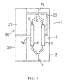
- Fig. 5 is a plan view of a further embodiment of this invention.
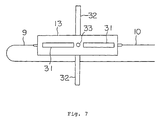
- Fig. 6 is a plan view of an electric field sensor having further antennas
- Fig. 7 is a side view of the sensor in Fig. 6.
- Fig. 8 is a perspective view of a further sensor having a plurality of antennas.
- an electric field sensor comprises a sensor head 1, a package 13 accommodating the sensor head 1, and' an antenna 14 attached to the outside of the package 13 and connected to the sensor head 1.
- the sensor head 1 has a substrate 3 and an optical modulator 4 attached to the substrate 3.
- the optical modulator 4 comprises an incident optical waveguide 5 formed on the substrate 3, two phase-shift optical waveguides 6 which are formed on the substrate 3 to be branched from the incident optical waveguide 5 and each of which has a variable refractive index varying in response to an electric field intensity applied thereto, an outgoing optical waveguide 7 formed on the substrate 3 to join the phase-shift optical waveguides 6, and two modulation electrodes 8 formed on or in the vicinity of the phase-shift optical waveguides 6.
- the incident optical waveguide 5 is connected to an incident optical fiber 9.
- the incident optical fiber 9 is connected to a light source 15.
- the light source 15 comprises a semiconductor laser.
- the outgoing optical waveguide 7 is connected to an outgoing optical fiber 10.
- the outgoing optical fiber 10 is connected to an optical detector 16.
- the antenna 14 comprises two rod antenna elements 17 and 18.
- the rod antenna elements 17 and 18 extend in opposite directions with their one ends located at a center portion of the package 13 and are arranged in parallel to the phase-shift optical waveguides 6.
- the rod antenna elements 17 and 18 are connected through lead' wires 19 and 20 to the modulation electrodes 8, respectively.
- a light beam from the light source 15 is incident through the incident optical fiber 9 to the incident optical waveguide 5 and branched by the two phase-shift optical waveguides 6 into branched beams which are again combined together in the outgoing optical waveguide 7.
- the light beam after being combined in the outgoing optical waveguide 7 is emitted through the outgoing optical fiber 10 to the optical detector 16.
- the modulation electrodes 8 apply predetermined electric fields to the phase-shift optical waveguides 6.
- the refractive indexes of the phase-shift optical waveguides 6 are varied. This results in variation of phases of the light beams transmitted through the phase-shift optical waveguides 6.
- the substrate 3 comprises a LiNbO 3 plate.
- the incident optical waveguide 5, the phase-shift optical waveguides 6, and the outgoing optical waveguide 7 are formed by thermal diffusion of Ti on a Z plane of the substrate 3.
- the incident optical fiber 9 comprises a constant-polarization optical fiber.
- the antenna 14 has two film antenna elements 22 and 23 fixedly attached to a side surface 21 of the package 13.
- the film antenna elements 22 and 23 extend in opposite directions with their one ends located at a center portion of the package 13 and are arranged in parallel to the phase-shift optical waveguides 6.
- the film antenna elements 22 and 23 are connected through lead wires 24 and 25 to the modulation electrodes 8, respectively.
- a still another embodiment illustrated in Fig. 4 has similar components depicted by the same reference numerals as those described in conjunction with the embodiment of Fig. 2.
- an antenna 26 has two film antenna elements 27 and 28 formed on the substrate 3 in parallel to the phase-shift optical waveguides 6.
- the film antenna elements 27 and 28 are arranged on both sides of the phase-shift optical waveguides 6.
- the film antenna elements 27 and 28 are connected through lead wires 29 and 30 to the modulation electrodes, respectively.
- the film antenna elements 27 and 28 may be arranged on one side of the phase-shift optical waveguides 6.
- the electric field sensor according to the embodiments illustrated in Figs. 4 and 5 it is possible to prevent a damage of the optical fiber because the draw-out portion of the optical fiber connected to the electric field sensor does not face the direction of measurement.
- the electric field sensor according to the embodiments in Figs. 4 and 5 are adapted to achieve reduction of size.
- an electric field sensor comprises the sensor head 1, the package 13 accommodating the sensor head 1, and antennas 31, 32, and 33 attached to the outside of the package 13 and connected to the sensor head 1.
- the sensor head 1 comprises a substrate 3 and a plurality of optical modulators 34, 35, and 36 attached to the substrate 3.
- Each of the optical modulators 34, 35, and 36 has the incident optical waveguide 5 formed on the substrate 3, the two phase-shift optical waveguides 6 which are formed on the substrate 3 to be branched from the incident optical waveguide 5 and each of which has a variable refractive index varying in response to the electric field intensity applied thereto, the outgoing optical waveguide 7 formed on the substrate 3 to join the phase-shift optical waveguides 6, and the two modulation electrodes 8 formed on or in the vicinity of the phase-shift optical waveguides 6.
- the incident optical waveguide 5 is connected to the incident optical fiber 9.
- the incident optical fiber 9 is connected to the light source 15.
- the outgoing optical waveguide 7 is connected to the outgoing optical fiber 10.
- the outgoing optical fiber 10 is connected to the optical detector 16.
- the antennas 31, 32, and 33 are arranged to be perpendicular to one another.
- the antennas 31, 32, and 33 are connected through the lead wires to the modulation electrodes 8 of the optical modulators 34, 35, and 36, respectively.
- each of the optical modulators 34, 35, and 36 has the incident optical waveguide 5 formed on the substrate 3, the two phase-shift optical waveguides 6 which are formed on the substrate 3 to be branched from the incident optical waveguide 5 and each of which has a variable refractive index varying in response to the electric field intensity applied thereto, the outgoing optical waveguide 7 formed on the substrate 3 to join the phase-shift optical waveguides 6, and the two modulation electrodes 8 formed on or in the vicinity of the phase-shift optical waveguides 6.
- the sensor head 1 has a common incident optical waveguide 37 connected to the incident optical fiber 9, primary branch optical waveguides 38 and 39 formed on the substrate 3 to be branched from the common incident optical waveguide 37, secondary branch optical waveguides 40 and 41 formed on the substrate 3 to be branched from the primary branch optical waveguide 38, and tertiary branch optical waveguides 42 and 43 formed on the substrate 3 to be branched from the primary branch optical waveguide 39.
- the secondary branch optical waveguide 40 is connected to the incident optical waveguide 5 of the optical modulator 34.
- the secondary branch optical waveguide 41 is connected to the incident optical waveguide 5 of the optical modulator 35.
- the tertiary branch optical waveguide 42 is connected to the incident optical waveguide 5 of the optical modulator 36.
- the tertiary branch optical waveguide 43 is connected through the outgoing optical fiber 10 to the optical detector 16.
- the light beam transmitted through the tertiary branch optical waveguide 43 is emitted through the outgoing optical fiber 10 to the optical detector 16.
- the light beam transmitted through the tertiary optical waveguide 43 is used as a reference light beam to monitor the light beam transmitted through the optical modulators 34, 35, and 36.
- Each of the embodiments illustrated in Figs. 6 through 8 has a plurality of antennas. It is therefore unnecessary to change the orientation in various directions during measurement. In addition, it is possible to carry out measurement independent from the incoming direction of the electromagnetic wave to be measured and from the polarization component.
- This invention is adapted for use in a device for measuring an intensity of an electric field such as an electromagnetic wave and electromagnetic noise.
Description
Claims (6)
- An electric field sensor comprising:characterized in thata sensor head (1) having a substrate (3) and an optical modulator (4) attached to said substrate (3),said optical modulator (4) comprising an incident optical waveguide (5) formed on said substrate (3), two phase-shift optical waveguides (6, 6) which are formed on said substrate (3) to be branched from said incident optical waveguide (5) and each of which has a variable refractive index varying in response to an electric field intensity applied thereto, an outgoing optical waveguide (7) formed on said substrate (3) to join said phase-shift optical waveguides (6, 6) and two modulation electrodes (8, 8) formed on and or in the vicinity of said phase-shift optical waveguides (6, 6);a package (13) accommodating said sensor head (1); andan antenna (14, 26) comprising two antenna elements (17, 18, 22, 23, 27, 28) connected to said two modulation electrodes (8, 8), respectively,
said two antenna elements (17, 18, 22, 23, 27, 28) extend in opposite directions in parallel with said phase-shift optical waveguides (6, 6) with their ends located at a center portion of said package. - An electric field sensor according to claim 1, wherein said two antenna elements are rod antenna elements (17, 18) mounted on an outside of said package (13).
- An electric field sensor according to claim 1, wherein said two antenna elements are film antenna elements (22, 23) formed on an outside surface (21) of said package (13).
- An electric field sensor according to claim 1, wherein said two antenna elements are film antenna elements (27, 28) formed on said substrate (3).
- An electric field sensor according to claim 4, wherein said film antenna elements (27, 28) are disposed at opposite sides with reference to said optical modulator (4), respectively.
- An electric field sensor according to claim 4, wherein said film antenna elements (27, 28) are disposed at the same side with reference to said optical modulator (4).
Applications Claiming Priority (10)
| Application Number | Priority Date | Filing Date | Title |
|---|---|---|---|
| JP5167857A JPH0720177A (en) | 1993-07-07 | 1993-07-07 | Optical field sensor |
| JP167857/93 | 1993-07-07 | ||
| JP167861/93 | 1993-07-07 | ||
| JP16786193 | 1993-07-07 | ||
| JP16786193A JPH0720178A (en) | 1993-07-07 | 1993-07-07 | Optical field sensor |
| JP16785793 | 1993-07-07 | ||
| JP53256/94 | 1994-02-25 | ||
| JP5325694 | 1994-02-25 | ||
| JP6053256A JPH07239356A (en) | 1994-02-25 | 1994-02-25 | Photoelectric field sensor |
| PCT/JP1994/001110 WO1995002193A1 (en) | 1993-07-07 | 1994-07-07 | Electric field sensor |
Publications (3)
| Publication Number | Publication Date |
|---|---|
| EP0668508A1 EP0668508A1 (en) | 1995-08-23 |
| EP0668508A4 EP0668508A4 (en) | 1996-09-11 |
| EP0668508B1 true EP0668508B1 (en) | 2002-06-05 |
Family
ID=27294891
Family Applications (1)
| Application Number | Title | Priority Date | Filing Date |
|---|---|---|---|
| EP94919869A Expired - Lifetime EP0668508B1 (en) | 1993-07-07 | 1994-07-07 | Electric field sensor |
Country Status (7)
| Country | Link |
|---|---|
| US (1) | US5488677A (en) |
| EP (1) | EP0668508B1 (en) |
| KR (1) | KR100220289B1 (en) |
| CN (1) | CN1052071C (en) |
| CA (1) | CA2144075C (en) |
| DE (1) | DE69430728T2 (en) |
| WO (1) | WO1995002193A1 (en) |
Families Citing this family (27)
| Publication number | Priority date | Publication date | Assignee | Title |
|---|---|---|---|---|
| JP3432957B2 (en) * | 1995-07-05 | 2003-08-04 | 三洋電機株式会社 | Optical modulator and optical fiber communication system |
| JP3411947B2 (en) * | 1995-08-08 | 2003-06-03 | シャープ株式会社 | Radio-to-optical conversion modulator and communication system using the same |
| US6252557B1 (en) * | 1999-09-30 | 2001-06-26 | Lockheed Martin Corporation | Photonics sensor array for wideband reception and processing of electromagnetic signals |
| US6686800B2 (en) | 2001-02-13 | 2004-02-03 | Quantum Applied Science And Research, Inc. | Low noise, electric field sensor |
| US7088175B2 (en) * | 2001-02-13 | 2006-08-08 | Quantum Applied Science & Research, Inc. | Low noise, electric field sensor |
| TW583399B (en) * | 2002-12-31 | 2004-04-11 | Ind Tech Res Inst | An optical sensor for electromagnetic field |
| US7015011B2 (en) * | 2003-04-18 | 2006-03-21 | Electronic Biosciences, Llc | Circuit and method to non-invasively detect the electrical potential of a cell or neuron |
| US6961601B2 (en) * | 2003-06-11 | 2005-11-01 | Quantum Applied Science & Research, Inc. | Sensor system for measuring biopotentials |
| CA2541981A1 (en) * | 2003-10-07 | 2005-06-09 | Quantum Applied Science And Research, Inc. | Integrated sensor system for measuring electric and/or magnetic field vector components |
| US7173437B2 (en) * | 2004-06-10 | 2007-02-06 | Quantum Applied Science And Research, Inc. | Garment incorporating embedded physiological sensors |
| US7245956B2 (en) * | 2004-07-15 | 2007-07-17 | Quantum Applied Science & Research, Inc. | Unobtrusive measurement system for bioelectric signals |
| US20060041196A1 (en) * | 2004-08-17 | 2006-02-23 | Quasar, Inc. | Unobtrusive measurement system for bioelectric signals |
| JP4751601B2 (en) * | 2004-09-30 | 2011-08-17 | 住友大阪セメント株式会社 | Light modulator |
| WO2007000947A1 (en) * | 2005-06-29 | 2007-01-04 | Nec Corporation | Electric field sensor, magnetic field sensor, electro-magnetic sensor, and electro-magnetic field measuring system using them |
| US7450790B1 (en) * | 2005-09-27 | 2008-11-11 | The Regents Of The University Of California | Non-electronic radio frequency front-end with immunity to electromagnetic pulse damage |
| WO2007094944A2 (en) * | 2006-02-13 | 2007-08-23 | Battelle Memorial Institute | Millimeter and sub-millimeter wave detection |
| US7486247B2 (en) | 2006-02-13 | 2009-02-03 | Optimer Photonics, Inc. | Millimeter and sub-millimeter wave detection |
| US7898464B1 (en) | 2006-04-11 | 2011-03-01 | Lockheed Martin Corporation | System and method for transmitting signals via photonic excitation of a transmitter array |
| US20080068182A1 (en) * | 2006-09-13 | 2008-03-20 | Brian Watson | Sensor for measuring relative conductivity changes in biological tissue |
| JP5439838B2 (en) * | 2009-02-10 | 2014-03-12 | 富士通オプティカルコンポーネンツ株式会社 | Light modulator |
| JP5487774B2 (en) * | 2009-07-27 | 2014-05-07 | 富士通オプティカルコンポーネンツ株式会社 | Optical device and optical transmitter |
| CN103605006B (en) * | 2013-11-13 | 2016-08-03 | 清华大学 | A kind of adjustable optical electric field sensor of antenna length |
| JP6728596B2 (en) * | 2015-08-21 | 2020-07-22 | セイコーエプソン株式会社 | Light modulator, optical module, and image display device |
| CN106680595B (en) * | 2015-11-11 | 2019-09-10 | 北京卫星环境工程研究所 | Double probe field measurement devices based on integrated light guide |
| CN106672890B (en) * | 2016-12-13 | 2018-12-04 | 北京中科飞龙传感技术有限责任公司 | A kind of encapsulation cover plate and packaging method of sensitivity reinforced electric field sensor |
| CN108957152B (en) * | 2018-07-02 | 2021-06-18 | 昆明理工大学 | Integrated optical waveguide electric field sensor system based on wavelength demodulation and measuring method thereof |
| CN109768391B (en) * | 2018-12-29 | 2020-12-15 | 京信通信技术(广州)有限公司 | Antenna, antenna electric downtilt display system and transmission mechanism thereof |
Family Cites Families (13)
| Publication number | Priority date | Publication date | Assignee | Title |
|---|---|---|---|---|
| DE2516619C2 (en) * | 1975-04-16 | 1983-12-01 | Siemens AG, 1000 Berlin und 8000 München | Device for measuring an electric or magnetic field |
| US4070621A (en) * | 1976-07-23 | 1978-01-24 | The United States Of America As Represented By The Department Of Health, Education And Welfare | Antenna with electro-optical modulator |
| EP0112945B1 (en) * | 1982-12-30 | 1987-05-06 | International Business Machines Corporation | Liquid filled electro-optic display cell and method of filling and sealing same |
| JPS59124366U (en) * | 1983-02-10 | 1984-08-21 | 横河電機株式会社 | light voltmeter |
| JPS59155764A (en) * | 1983-02-24 | 1984-09-04 | Yokogawa Hokushin Electric Corp | Photovoltometer |
| US5021731A (en) * | 1989-02-21 | 1991-06-04 | Metricor, Inc. | Thermo-optical current sensor and thermo-optical current sensing systems |
| JPH0670653B2 (en) * | 1989-03-31 | 1994-09-07 | 日本碍子株式会社 | Light temperature / electric quantity measuring device |
| US5008678A (en) * | 1990-03-02 | 1991-04-16 | Hughes Aircraft Company | Electronically scanning vehicle radar sensor |
| IT1248820B (en) * | 1990-05-25 | 1995-01-30 | Pirelli Cavi Spa | FIELD DIRECTIONAL POLARIMETRIC SENSOR |
| JP2619981B2 (en) * | 1990-11-06 | 1997-06-11 | 株式会社豊田中央研究所 | Electromagnetic field strength measuring device |
| JPH04332878A (en) * | 1991-05-07 | 1992-11-19 | Toyota Central Res & Dev Lab Inc | Electromagnetic field intensity measuring device |
| US5267336A (en) * | 1992-05-04 | 1993-11-30 | Srico, Inc. | Electro-optical sensor for detecting electric fields |
| US5402259A (en) * | 1993-04-23 | 1995-03-28 | Trw Inc. | Linear electroabsorptive modulator and related method of analog modulation of an optical carrier |
-
1994
- 1994-07-07 WO PCT/JP1994/001110 patent/WO1995002193A1/en active IP Right Grant
- 1994-07-07 EP EP94919869A patent/EP0668508B1/en not_active Expired - Lifetime
- 1994-07-07 DE DE69430728T patent/DE69430728T2/en not_active Expired - Fee Related
- 1994-07-07 CN CN94190478A patent/CN1052071C/en not_active Expired - Fee Related
- 1994-07-07 US US08/397,076 patent/US5488677A/en not_active Expired - Lifetime
- 1994-07-07 KR KR1019950700890A patent/KR100220289B1/en not_active IP Right Cessation
- 1994-07-07 CA CA002144075A patent/CA2144075C/en not_active Expired - Fee Related
Also Published As
| Publication number | Publication date |
|---|---|
| EP0668508A1 (en) | 1995-08-23 |
| DE69430728D1 (en) | 2002-07-11 |
| CN1052071C (en) | 2000-05-03 |
| DE69430728T2 (en) | 2002-12-05 |
| CA2144075A1 (en) | 1995-01-19 |
| KR950703153A (en) | 1995-08-23 |
| US5488677A (en) | 1996-01-30 |
| CN1111917A (en) | 1995-11-15 |
| CA2144075C (en) | 2002-01-08 |
| KR100220289B1 (en) | 1999-09-15 |
| WO1995002193A1 (en) | 1995-01-19 |
| EP0668508A4 (en) | 1996-09-11 |
Similar Documents
| Publication | Publication Date | Title |
|---|---|---|
| EP0668508B1 (en) | Electric field sensor | |
| EP0664460B1 (en) | Electric field sensor | |
| US5625284A (en) | Electric field sensor having sensor head with unbalanced electric field shield to shield branched optical waveguides against an applied electric field | |
| FI115077B (en) | Controllable polarization transformer | |
| US7783138B2 (en) | Free-space integrated photodetector with reduced phase tracking error | |
| US5029273A (en) | Integrated optics Pockels cell voltage sensor | |
| CA2149267A1 (en) | Electric field sensor | |
| KR20010013957A (en) | Method and apparatus for switching, amplification, control and modulation | |
| KR100496309B1 (en) | Optical modulation device equipped with a reflector plate slanting against a reflective side plane of an optical waveguide path | |
| US5107535A (en) | Connecting method between waveguide substrate and optical fiber | |
| CA2091499C (en) | Large angle broadband multilayer deflectors | |
| US11125943B2 (en) | Optical modulator and optical measurement apparatus | |
| JP2004212137A (en) | Triaxial photoelectric field sensor | |
| JP2002181861A (en) | Electric field sensor unit | |
| JP2673485B2 (en) | Electric field detection method | |
| JP3404604B2 (en) | Optical electric field sensor | |
| JPH01102506A (en) | Laminated waveguide type optical device element | |
| JPH0315831A (en) | Light deflecting element | |
| JPS60257325A (en) | Photovoltage sensor | |
| JP3145798B2 (en) | Optical magnetic field sensor and magnetic field measuring device | |
| JP3355502B2 (en) | Electric field sensor | |
| JP3673611B2 (en) | Electric field sensor | |
| KR19980016030A (en) | Polymer optical waveguide polarizer | |
| JP3435584B2 (en) | Electric field sensor head and electric field sensor | |
| Chen et al. | A Microprism Array for Large-Scale, Wide-Band Interconnection of Optoelectronic Systems |
Legal Events
| Date | Code | Title | Description |
|---|---|---|---|
| PUAI | Public reference made under article 153(3) epc to a published international application that has entered the european phase |
Free format text: ORIGINAL CODE: 0009012 |
|
| 17P | Request for examination filed |
Effective date: 19950306 |
|
| AK | Designated contracting states |
Kind code of ref document: A1 Designated state(s): DE FR GB IT |
|
| RHK1 | Main classification (correction) |
Ipc: G01R 15/24 |
|
| A4 | Supplementary search report drawn up and despatched | ||
| AK | Designated contracting states |
Kind code of ref document: A4 Designated state(s): DE FR GB IT |
|
| 17Q | First examination report despatched |
Effective date: 19990721 |
|
| GRAG | Despatch of communication of intention to grant |
Free format text: ORIGINAL CODE: EPIDOS AGRA |
|
| GRAG | Despatch of communication of intention to grant |
Free format text: ORIGINAL CODE: EPIDOS AGRA |
|
| GRAH | Despatch of communication of intention to grant a patent |
Free format text: ORIGINAL CODE: EPIDOS IGRA |
|
| GRAH | Despatch of communication of intention to grant a patent |
Free format text: ORIGINAL CODE: EPIDOS IGRA |
|
| GRAA | (expected) grant |
Free format text: ORIGINAL CODE: 0009210 |
|
| AK | Designated contracting states |
Kind code of ref document: B1 Designated state(s): DE FR GB IT |
|
| REG | Reference to a national code |
Ref country code: GB Ref legal event code: FG4D |
|
| REF | Corresponds to: |
Ref document number: 69430728 Country of ref document: DE Date of ref document: 20020711 |
|
| RAP2 | Party data changed (patent owner data changed or rights of a patent transferred) |
Owner name: NEC TOKIN CORPORATION |
|
| ET | Fr: translation filed | ||
| PLBE | No opposition filed within time limit |
Free format text: ORIGINAL CODE: 0009261 |
|
| STAA | Information on the status of an ep patent application or granted ep patent |
Free format text: STATUS: NO OPPOSITION FILED WITHIN TIME LIMIT |
|
| 26N | No opposition filed |
Effective date: 20030306 |
|
| PGFP | Annual fee paid to national office [announced via postgrant information from national office to epo] |
Ref country code: GB Payment date: 20040707 Year of fee payment: 11 |
|
| PGFP | Annual fee paid to national office [announced via postgrant information from national office to epo] |
Ref country code: FR Payment date: 20040708 Year of fee payment: 11 |
|
| PGFP | Annual fee paid to national office [announced via postgrant information from national office to epo] |
Ref country code: DE Payment date: 20040715 Year of fee payment: 11 |
|
| PG25 | Lapsed in a contracting state [announced via postgrant information from national office to epo] |
Ref country code: IT Free format text: LAPSE BECAUSE OF NON-PAYMENT OF DUE FEES;WARNING: LAPSES OF ITALIAN PATENTS WITH EFFECTIVE DATE BEFORE 2007 MAY HAVE OCCURRED AT ANY TIME BEFORE 2007. THE CORRECT EFFECTIVE DATE MAY BE DIFFERENT FROM THE ONE RECORDED. Effective date: 20050707 Ref country code: GB Free format text: LAPSE BECAUSE OF NON-PAYMENT OF DUE FEES Effective date: 20050707 |
|
| PG25 | Lapsed in a contracting state [announced via postgrant information from national office to epo] |
Ref country code: DE Free format text: LAPSE BECAUSE OF NON-PAYMENT OF DUE FEES Effective date: 20060201 |
|
| GBPC | Gb: european patent ceased through non-payment of renewal fee |
Effective date: 20050707 |
|
| PG25 | Lapsed in a contracting state [announced via postgrant information from national office to epo] |
Ref country code: FR Free format text: LAPSE BECAUSE OF NON-PAYMENT OF DUE FEES Effective date: 20060331 |
|
| REG | Reference to a national code |
Ref country code: FR Ref legal event code: ST Effective date: 20060331 |