EP0660938B1 - Full and partial cycle counting apparatus and method - Google Patents
Full and partial cycle counting apparatus and method Download PDFInfo
- Publication number
- EP0660938B1 EP0660938B1 EP93921583A EP93921583A EP0660938B1 EP 0660938 B1 EP0660938 B1 EP 0660938B1 EP 93921583 A EP93921583 A EP 93921583A EP 93921583 A EP93921583 A EP 93921583A EP 0660938 B1 EP0660938 B1 EP 0660938B1
- Authority
- EP
- European Patent Office
- Prior art keywords
- sample period
- leading edge
- signal
- cycles
- output
- Prior art date
- Legal status (The legal status is an assumption and is not a legal conclusion. Google has not performed a legal analysis and makes no representation as to the accuracy of the status listed.)
- Expired - Lifetime
Links
Images

Classifications
-
- G—PHYSICS
- G01—MEASURING; TESTING
- G01R—MEASURING ELECTRIC VARIABLES; MEASURING MAGNETIC VARIABLES
- G01R23/00—Arrangements for measuring frequencies; Arrangements for analysing frequency spectra
- G01R23/02—Arrangements for measuring frequency, e.g. pulse repetition rate; Arrangements for measuring period of current or voltage
- G01R23/10—Arrangements for measuring frequency, e.g. pulse repetition rate; Arrangements for measuring period of current or voltage by converting frequency into a train of pulses, which are then counted, i.e. converting the signal into a square wave
-
- G—PHYSICS
- G01—MEASURING; TESTING
- G01P—MEASURING LINEAR OR ANGULAR SPEED, ACCELERATION, DECELERATION, OR SHOCK; INDICATING PRESENCE, ABSENCE, OR DIRECTION, OF MOVEMENT
- G01P15/00—Measuring acceleration; Measuring deceleration; Measuring shock, i.e. sudden change of acceleration
- G01P15/02—Measuring acceleration; Measuring deceleration; Measuring shock, i.e. sudden change of acceleration by making use of inertia forces using solid seismic masses
- G01P15/08—Measuring acceleration; Measuring deceleration; Measuring shock, i.e. sudden change of acceleration by making use of inertia forces using solid seismic masses with conversion into electric or magnetic values
- G01P15/097—Measuring acceleration; Measuring deceleration; Measuring shock, i.e. sudden change of acceleration by making use of inertia forces using solid seismic masses with conversion into electric or magnetic values by vibratory elements
-
- G—PHYSICS
- G01—MEASURING; TESTING
- G01P—MEASURING LINEAR OR ANGULAR SPEED, ACCELERATION, DECELERATION, OR SHOCK; INDICATING PRESENCE, ABSENCE, OR DIRECTION, OF MOVEMENT
- G01P3/00—Measuring linear or angular speed; Measuring differences of linear or angular speeds
- G01P3/42—Devices characterised by the use of electric or magnetic means
- G01P3/44—Devices characterised by the use of electric or magnetic means for measuring angular speed
- G01P3/48—Devices characterised by the use of electric or magnetic means for measuring angular speed by measuring frequency of generated current or voltage
- G01P3/481—Devices characterised by the use of electric or magnetic means for measuring angular speed by measuring frequency of generated current or voltage of pulse signals
- G01P3/489—Digital circuits therefor
Definitions
- the present invention relates to a method and apparatus for accurately counting the number of cycles and partial cycles occurring in a frequency modulated electrical signal during a sample period. More particularly the invention relates to a method and apparatus for determining the incremental change in velocity experienced by the accelerometer by counting cycles in two outputs of a digital accelerometer during a sample period.
- a type of accelerometer described by a Peters patent US-A-4,712,427 operates to produce four digital outputs. Two of these outputs are in the form of acceleration dependent frequency modulated signals. The other two outputs provide information concerning temperature and calibration coefficients respectively. To calculate the incremental change in velocity being experienced one may determine the changes in frequency between the first two outputs and provide adjustments in accordance with the second two outputs. Determining frequency changes is sometimes accomplished by means of a counter which counts the number of cycles of each output during a sample period. To obtain high accuracy, it is not only necessary to count the number of full cycles during a sample period but also any portions of a cycle which occur during that period. Having the number of full and partial cycles of the two acceleration dependent frequency modulated outputs, the average frequency during the sample period may then be numerically converted by a system processor to calculate the incremental velocity along the sensing axis of the accelerometer.
- a full and partial cycle counting apparatus has been described in the Hulsing II, et al patent US-A-4,786,861 which employs a first counter operable to provide an output count indicative of the number of full cycles in a sampling period defined by two successive strobe signals, a second counter which counts the integer number of high frequency clock cycles occurring during a full cycle of the unknown frequency and a third counter which counts the integer number of high frequency clock cycles during a time period starting with the end of the sample period and ending with the next rising edge of the signal being measured. Subtracting the ratio of the number of high frequency clock cycles during this latter time period to the number of high frequency counts during a full cycle from 1 is indicative of the portion of a full cycle that occurs before the end of the sample period. The ratio defined above indicates the portion of a full cycle that occurs after the start of the next sample period.
- a problem encountered in the above described apparatus arises from the fact that it is necessary to wait until after the end of a sample period to determine the number of high frequency clock periods existing in a portion of a cycle of the signal being measured. As a result, the information used to determine the incremental change in velocity along the sensing axis cannot be sent to the system processor for use until after the completion of the full cycle of the unknown frequency which was initiated prior to the end of the subsequent sample period.
- the apparatus and method known from US-A-3 829 785 provide a measurement of the unknown frequency of a pulsed signal. Account is taken in this measurement of the partial cycles of the signal occurring prior to and at the end of the measurement interval.
- the present invention provides an apparatus and method for determining the number of full and partial cycles occurring during a sample period of a frequency modulated digital electric signal and obtains this information during the sample period so that it may be sent to the system processor immediately after the start of the next sample period.
- a digital accelerometer 10 which may be of the type shown in the above referred to patent US-A-4,712,427 is shown producing 4 outputs, F 1 , F 2 , F T and CC.
- F 1 is the first frequency output indicative of acceleration
- F 2 is the second frequency output indicative of acceleration
- F T is a frequency output indicative of the temperature of the digital accelerometer
- CC is the serial data output of the digital accelerometer calibration coefficients. It will be understood that if the digital accelerometer is experiencing no acceleration, then the frequency of the outputs F 1 and F 2 will each be equal to a respective nominal value but as acceleration is experienced along the sensing axis the frequency of both F 1 and F 2 will change in magnitude.
- the changes in frequency of F 1 and F 2 are of opposite polarity and are approximately proportional to acceleration along the sensing axis.
- the temperature output F T is a frequency modulated digital output used by the system processor to adjust the system for incremental changes in temperature.
- the output CC is a standard serial data output used to transmit the calibration coefficients which are used to reduce the effects of bias error and gain error and the effects of nonlinearity errors, and will not be further described herein.
- the output F 1 is shown being presented on a line 12 to an (ASIC) 14.
- Output F 2 is presented to ASIC 14 on a line 16 while output F T is presented to ASIC 14 on a line 18 and the serial data output CC is presented to ASIC 14 on a line 20.
- a strobe input 22 is shown producing a signal to ASIC 14 via a line 24 and the strobe signal comprises a series of periodic pulses used to determine a sample period for finding the frequency variations of the signals F 1 and F 2 .
- a high frequency clock 25 is also shown producing an input to ASIC 14 by a line 26.
- the strobe signal 22 is asynchronous with respect to high frequency clock 25.
- ASIC 14 contains circuitry which will be described in connection with Figure 3 to produce a plurality of outputs on a line 28 which are presented to a system processor 30.
- the signals on line 28 will be serial or parallel data signals indicative of the various outputs produced by the circuitry of Figure 3 and the system processor 30 will operate on the signals to produce an output on a line 32 indicative of the incremental change in velocity being experienced by the digital accelerometer 10 along the sensing axis.
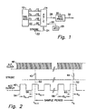
- one of the outputs, F 1 or F 2 of the digital accelerometer 10 is shown as a series of cycles described by a square wave 40 at the lower portion of Figure 2.
- a single sample period is shown existing between the rising edge of a first strobe pulse 42 and the rising edge of the next following strobe pulse 44 and it is during this sample period that it is desired to determine the number of full and partial cycles of the accelerometer output signal 40.
- Also shown in Figure 2 is the output of a high frequency clock shown by a plurality of square wave pulses 46.
- a vertical dash line 50 has been drawn at the rising edge of pulse 42 to define the start of the sample period and a vertical dash line 52 has been drawn at the rising edge of pulse 44 to define the end of the sample period and these two vertical dash lines describe the sample period from time t n-1 to t n .
- a vertical dash line 54 is shown corresponding to the first rising edge of the last complete cycle of the accelerometer output occurring prior to the start of the sample period and a dash line 56 is shown corresponding to the rising edge of the accelerometer output 40 occurring just before the sample period. The distance between lines 54 and 56 is indicative of the time for one complete cycle and this is denoted D n-1 in Figure 2.
- a similar vertical dash line 58 is shown corresponding to the first rising edge of the last complete cycle of the accelerometer output signal 40 occurring before the end of the sample period and a similar dash line 60 is shown corresponding to the last rising edge of the accelerometer output signal 40 occurring before the end of the sample period.
- the distance between lines 58 and 60 is indicative of the time for one complete cycle in the accelerometer output 40 and this has been denoted D n in Figure 2. It should be noted that D n is not necessarily equal to D n-1 since during the sample period the acceleration can cause the compression or expansion of the length of time of a full cycle.
- This value is obtained by a first counter in Figure 3 which receives the accelerometer output signal 40 of Figure 2 and continuously counts the number of leading edges, LE, that occur where each leading edge of accelerometer output signal 40 is a rising edge of signal 40.
- the output value of the LE counter, at the end of each sample period is sent to the system processor.
- the system processor uses the output value of the leading edge counter at the completion of the previous sample period (LE n ) and subtracts from this the output value of the leading edge counter at the start of the previous sample period (LE n-1 ). This difference, less 1, is the number of full cycles in the last complete sample period.
- a second counter counts the number of high frequency clock pulses 46 which occur during the periods D n-1 and D n and which occur during the periods N n-1 and N n .
- N T (LE n -LE n-1 -1) + N n /D n + (1-N n-1 /D n-1)
- N T LE n -LE n-1 + N n /D n - N n-1 /D n-1
- Figure 3 shows a circuit operable to count the various full and partial cycles present in the two frequency modulated acceleration dependent outputs of the digital accelerometer in order to arrive at the values suitable for the system processor to solve equation 2.
- a pulse accumulator enclosed by dash lines 70 receiving a first input from a box 72 labeled F 1 on a line 74.
- Box 72 on line 74 corresponds to the output F 1 identified on line 12 of Figure 1.
- a second input to pulse accumulator 70 is shown being derived from a box 76, a high frequency clock generator, on a line 78 via three branches on lines 80, 82, and 84.
- the output from clock 76 on line 78 will be like that shown as the high frequency clock pulse signal 46 in Figure 2.
- An input from a strobe box 88 is presented on a line 90 as another input to the pulse accumulator 70 and this signal will correspond to the signal represented as the strobe signal with pulses 42 and 44 in Figure 2.
- a reset pulse RS originating from a source (not shown) is presented to various components in the pulse accumulator 70 at terminals labeled RS on lines 92, 93, 94, 95, 96, and 97 in Figure 3 and these signals operate to reset the various components at the beginning of or start up of the operation and will not be further described.
- An enable circuit box 100 is shown in Figure 3 receiving an input from strobe 88 via line 90 and a line 101.
- the enable circuit 100 operates to produce a plurality of separate outputs E 1 , E 2 , E 3 , E 4 , E 5 , E 6 , E 7 , and E 8 for use by various of the components in Figure 3 as will be explained.
- a first of the outputs E 1 of enable circuit 100 is connected to a terminal 106 at the top of accumulator 70 but, for simplicity, the line showing the connection is not drawn.
- output E 2 is connected to line 107 and output E 3 is connected to line 108 by connecting lines not shown.
- a disenable box 110 is shown in Figure 3 receiving an input E 8 from the enable box 100 over a line 112 and receiving an input from the strobe box 88 over line 114 to produce an output on a line 116 as an input to pulse accumulator 70 for purpose to be explained later.
- a synchronizer box 120 receiving the first frequency F 1 on line 74 and receiving a clock input from clock 76 on line 80.
- the synchronizer 120 which may be of standard design, operates to provide a logic 1 output pulse as an output signal F S1 on a line 122 with a pulse width equal to 1 high frequency clock period; the logic 1 output pulse is initiated on the first rising edge of the high frequency clock following a rising edge occurence on F 1 , on line 74.
- the synchronizer 120 operates to alter the leading edges of the signal in F 1 so that they occur simultaneously with the leading edge of a clock signal.
- the output F S1 on line 122 will not have leading edges of the variable frequency input occurring randomly through one of the clock cycles but rather they will occur as close as possible after the clock rising edge.
- the output on line 122 of the synchronizer 120 is presented to a leading edge counter shown as box 125 which also receives an input from the clock 76 over line 82 and which operates, after initially being cleared by the reset signal on line 93, to count the leading edges in the signal F S1 . It does this by utilizing, for example, 16 synchronous D-flip flops which provide a parallel output on a line 130 digitally representative of the number of rising edges of the F S1 signal which is accumulated in the counter 125.
- Utilizing 16 D-flip flops gives the counter the capability of counting 2 16 or 65,536 leading edges which is far more than the number of leading edges possible in the signal F S1 during a sample period.
- the parallel output which is constantly changing with each rising edge of the input signal on line 122 is presented by line 130 to a leading edge store or memory box 133 which also contains 16 D-flip flops that are set in accordance with the signal on line 130.
- the logic states of the 16 D-flip flop outputs in the leading edge storage 133 are set to equal the logic state of the leading edge counter 125 16 bit parallel output over line 130 and these logic states are held until released to the system processor.
- the enable circuit 100 which receives an input from the strobe 88 over lines 90 and 101 operates to produce the output E 1 in a timed sequence to the leading edge store box 133 over line 106 at a predetermined time after the end of a sample period as determined by the occurrence of a strobe signal from box 88.
- This signal E 1 over line 106 allows the leading edge store box 133 to release the information it has stored in the D-flip flops therein as a serial or parallel output signal LE 1 on line 150.
- This output signal on line 150 will provide the information indicative of the number of leading edges accumulated in the leading edge counter 125 after the end of the previous sample period. This information is then presented to the system processor for use in solving equation 2 above.
- the synchronized output F S1 from the synchronizer 120 is presented by a line 152 and a line 154 to one of the inputs of an or gate 156 whose other input is received via line 95 from the reset signal.
- a logic 1 state from either the reset input or from the synchronized signal F S1 will produce a logic 1 output state from or gate 156 on a line 158.
- a signal on line 158 is presented to a second leading edge counter 160 and operates to reset the 16 D-flip flops therein if in the logic 1 state and will allow them to start counting if in the logic 0 state.
- the second leading edge counter 160 also receives the high frequency clock output from clock box 76 over lines 78 and 84.
- the flip flops in leading edge counter 160 will produce a parallel output indicative of the number of leading edges counted in the high frequency clock signal. Since this count begins starting with each leading edge in the synchronized signal F S1 the LE counter 160 will provide a parallel output on a line 162 indicative of the number of high frequency clock cycles that have occurred since the last leading edge of the synchronized output F S1 ⁇
- This signal is presented to an "N" store box 165 which, like the leading edge store box 133, contains 16 D-flip flops which will be set by the output of the leading edge counter 160.
- This count is set by the signal from the strobe 88 via lines 90, inverter 140, line 142, and a line 167 at which time the count is held in the N store box 165.
- This signal is released in serial or parallel fashion on output line 168 upon the occurrence of a E 2 signal on line 107.
- the E 2 signal to N store box 165 will not occur at the same time as the E 1 signal on line 106 above described but rather, all of the signals E 1 -E 8 are in timed sequence so as to allow the output 168 from the N store box 165 to be released at a different time than the output 150 from the leading edge store box 133. This occurs very rapidly, however, and the entire output from all of the various store boxes of the circuit of Figure 3 can be presented to the system processor in far less than the time of a sample period between two strobe pulses.
- the output on line 168 is indicative of N 1 which is the number of high frequency clock cycles occurring from the time of the last leading edge in the synchronized signal F S1 prior to the occurrence of the rising edge of the strobe pulse, 52 in Figure 2.
- N 1 is the number of high frequency clock cycles occurring from the time of the last leading edge in the synchronized signal F S1 prior to the occurrence of the rising edge of the strobe pulse, 52 in Figure 2.
- the N 1 output on line 168 will be used by the system processor 30 of Figure 1 in solving the equation 2 above.
- the synchronized output F S1 from the synchronizer 120 is also presented via lines 152 and a line 170 to one of the inputs of an and gate 172 whose other input is received from the disenabler 110 via line 116, inverter 174 and a line 176.
- a logic 1 state exists at the output from and gate 172 on a line 180 whenever a logic 1 state exists in both the synchronized output F S1 and the inverted disenable signal from inverter 174 on line 176.
- the disenabler 110 is seen to receive an input E 8 from the enabler 100 on a line 112 and it operates to provide an output on line 116 which will be a logic 1 state until such time as the enabler 100 provides a signal indicating that the two outputs D 1 and D 2 from the D store boxes such as 186 and the D store box within pulse accumulator 200 to be described have presented their outputs to the system processor.
- the purpose of this is to prevent a logic 1 state output on line 180 until after the system processor has received all of the information stored in the D store boxes for the previous sample period.
- the signal on line 180 is presented to an inverter 182 to provide an output on line 184 to a D store box 186 which also receives the output from the leading edge counter 160 via lines 162 and a line 190.
- the D store box 186 like the leading edge store and the N store boxes above described contains 16 D-flip flops which follow the output from the leading edge counter 160 so as to store the information indicative of the number of high frequency clock cycles occurring since the last leading edge in the synchronized signal F S1 until such time as an input on line 184 causes the D store 186 to hold or store the value of the leading edge counter 160.
- the output states of the D-flip flops in the D store box 186 are held in storage upon the occurrence of a logic 1 state on line 184 and like the LE store box 133 and the N store box 165 will release the D 1 signal stored in serial or parallel fashion on output line 194 upon the occurrence of the "E 3 " signal on line 108. Thereafter, both the D store box 186 and the D store box within pulse accumulator 200, will not be loaded by the output from the respective LE counter during the time from the last leading edge of the strobe signal on line 114 until such time as the disenabler 110 has received an "E 8 " signal from the enabler circuit 100 telling it that the sequence of sending the contents of the D store boxes to the system processor is completed.
- the D store boxes will again assume the values of the outputs of the LE counters at the next leading edge occurence of the F s1 signal. It is seen that the D store box receives information concerning a whole cycle only.
- the E 3 signal on line 108 enables the contents of the D store box 186 to be released in serial or parallel fashion, the D storage box will be holding the count from the last complete cycle in the F S1 signal prior to the occurrence of the completion of the sample period determined by the next leading edge of the strobe signal.
- This D 1 signal is released in serial or parallel fashion on a line 194 in a sequence with the previously described signals LE 1 and N 1 from lines 150 and 168.
- serial outputs on line 150, 168, and 194 are presented to the system processor in a way that do not overlap by virtue of the timing of the E 1 , E 2 and E 3 signals and that these serial outputs are indicative of LE 1 , N 1 , and D 1 for use by the system processor in determining the solution to the equation 2 above.
- the information transmitted to the system processor at the start of the last sample period is, in fact, this information.
- the system processor therefore stores the information at the end of a sample period and then receives the information from the end of the next sample period and has all of the necessary information for use in solving equation 2 for the first signal F 1 .
- Pulse accumulator 200 is the same as pulse accumulator 70 and receives the same reset signals on lines 202, 203, and 204 as was received by the pulse accumulator 70. Pulse accumulator 200 also receives a second frequency input from box 210 via an input line 212 to provide the pulse accumulator 200 with a second frequency input signal, F 2 , shown in Figure 1. Box 210 on line 212 corresponds to the output F 2 identified on line 16 of Figure 1.
- Pulse accumulator 200 also receives inputs E 4 , Eg and E 6 from the enable circuit 100 over a lines 214, 215 and 216 and an input from the disenable circuit 110 via lines 116 and a line 217, a clock input signal from the clock 76 via lines 78 and 218 and a strobe signal from the strobe 88 via lines 90 and 220. Accordingly the pulse accumulator 200, which contains the same circuitry as shown in connection with pulse accumulator 70, will operate in the same manner to produce three outputs on lines 222, 224, and 226 indicative of the values LE 2 , N 2 , and D 2 to the system processor 30 in a manner similar to that shown in connection with the pulse accumulator 70. The pulse accumulator 200 will also have transmitted information produced after the last sample period to the system processor and accordingly the system processor will have the LE n-1 N n-1 and D n-1 values available necessary for use in solving the equation 2, above for the second signal F 2 .
- the two pulse accumulators 70 and 200 of Figure 3 provide the necessary information for the system processor 30 of Figure 1 to solve equation 2 for both F 1 and F 2 and then to numerically determine and produce an output signal indicative of the incremental change in velocity along the sensing axis on line 32 in Figure 1. It should also be noticed that this information can be transmitted to the system processor at a point in time just after the occurrence of a strobe pulse 44 without waiting for the accumulation of further data thereafter as was necessary in the above referred to prior art patent US-A-4 786 861.
- FIG. 3 a system for determining the number of full cycles in a frequency modulated signal indicative of the temperature of the digital accelerometer is shown comprising a third pulse accumulator shown by dash lines 240 receiving an input from the source of the frequency modulated signal indicative of temperature box 242 whose output is on a line 244. Box 242 on line 244 corresponds to the output F T identified on line 18 of Figure 1.
- this signal is fed to a synchronizer 250 so that after a reset signal from line 252 is received, synchronizer 250 may alter the leading edge of the signal on line 244 so that it coincides with the next leading edge of a high frequency clock cycle presented from clock circuit 76 via line 78 and 256 to provide an output on a line 258 indicative of a synchronized signal F ST .
- This signal is fed to a leading edge counter 262 which also receives a high frequency clock input via lines 78 and 264 so that after being reset by a reset signal on line 266, leading edge counter 262 provides an output on a line 268 indicative of the number of leading edges which occur in the signal F ST .
- the loading of the output states of the 16 D-flip flops within the temperature store box 272 is controlled by a signal from the strobe box 88 via lines 90 and 276, inverter 278 and a line 280 so that the accumulated count from the leading edge counter 262 is loaded and stored at the end of each sample period. This count is released in serial or parallel fashion on a line 284 upon the occurrence of an enable signal E 7 on line 286 to the T store box 272.
- a signal LE T is presented to the system processor via line 284, to determine the incremental change in frequency of the F T signal during a sample period.
- N T LE n -LE n-1 -1
Landscapes
- Physics & Mathematics (AREA)
- General Physics & Mathematics (AREA)
- Measuring Frequencies, Analyzing Spectra (AREA)
- Transmission And Conversion Of Sensor Element Output (AREA)
Abstract
Description
- The present invention relates to a method and apparatus for accurately counting the number of cycles and partial cycles occurring in a frequency modulated electrical signal during a sample period. More particularly the invention relates to a method and apparatus for determining the incremental change in velocity experienced by the accelerometer by counting cycles in two outputs of a digital accelerometer during a sample period.
- In the art of sensing acceleration, a type of accelerometer described by a Peters patent US-A-4,712,427 operates to produce four digital outputs. Two of these outputs are in the form of acceleration dependent frequency modulated signals. The other two outputs provide information concerning temperature and calibration coefficients respectively. To calculate the incremental change in velocity being experienced one may determine the changes in frequency between the first two outputs and provide adjustments in accordance with the second two outputs. Determining frequency changes is sometimes accomplished by means of a counter which counts the number of cycles of each output during a sample period. To obtain high accuracy, it is not only necessary to count the number of full cycles during a sample period but also any portions of a cycle which occur during that period. Having the number of full and partial cycles of the two acceleration dependent frequency modulated outputs, the average frequency during the sample period may then be numerically converted by a system processor to calculate the incremental velocity along the sensing axis of the accelerometer.
- A full and partial cycle counting apparatus has been described in the Hulsing II, et al patent US-A-4,786,861 which employs a first counter operable to provide an output count indicative of the number of full cycles in a sampling period defined by two successive strobe signals, a second counter which counts the integer number of high frequency clock cycles occurring during a full cycle of the unknown frequency and a third counter which counts the integer number of high frequency clock cycles during a time period starting with the end of the sample period and ending with the next rising edge of the signal being measured. Subtracting the ratio of the number of high frequency clock cycles during this latter time period to the number of high frequency counts during a full cycle from 1 is indicative of the portion of a full cycle that occurs before the end of the sample period. The ratio defined above indicates the portion of a full cycle that occurs after the start of the next sample period.
- A problem encountered in the above described apparatus, arises from the fact that it is necessary to wait until after the end of a sample period to determine the number of high frequency clock periods existing in a portion of a cycle of the signal being measured. As a result, the information used to determine the incremental change in velocity along the sensing axis cannot be sent to the system processor for use until after the completion of the full cycle of the unknown frequency which was initiated prior to the end of the subsequent sample period.
- The apparatus and method known from US-A-3 829 785 provide a measurement of the unknown frequency of a pulsed signal. Account is taken in this measurement of the partial cycles of the signal occurring prior to and at the end of the measurement interval.
- The present invention provides an apparatus and method for determining the number of full and partial cycles occurring during a sample period of a frequency modulated digital electric signal and obtains this information during the sample period so that it may be sent to the system processor immediately after the start of the next sample period.
-
- Figure 1 shows a block diagram of the system involving the digital accelerometer, the application specific integrated circuit (ASIC) which contains the counting apparatus of the present invention and, the system processor;
- Figure 2 is a timing diagram showing the relationship between one of the outputs of the digital accelerometer, the high frequency clock and the asynchronous strobe input defining a sample period; and,
- Figure 3 is a block schematic diagram of the apparatus for accurately counting the quantity of full and partial cycles occurring during a sample period in the outputs of the digital accelerometer.
- In Figure 1 a
digital accelerometer 10 which may be of the type shown in the above referred to patent US-A-4,712,427 is shown producing 4 outputs, F1, F2, FT and CC. F1 is the first frequency output indicative of acceleration, F2 is the second frequency output indicative of acceleration, FT is a frequency output indicative of the temperature of the digital accelerometer, and CC is the serial data output of the digital accelerometer calibration coefficients. It will be understood that if the digital accelerometer is experiencing no acceleration, then the frequency of the outputs F1 and F2 will each be equal to a respective nominal value but as acceleration is experienced along the sensing axis the frequency of both F1 and F2 will change in magnitude. The changes in frequency of F1 and F2 are of opposite polarity and are approximately proportional to acceleration along the sensing axis. The temperature output FT is a frequency modulated digital output used by the system processor to adjust the system for incremental changes in temperature. The output CC is a standard serial data output used to transmit the calibration coefficients which are used to reduce the effects of bias error and gain error and the effects of nonlinearity errors, and will not be further described herein. - The output F1 is shown being presented on a line 12 to an (ASIC) 14. Output F2 is presented to ASIC 14 on a
line 16 while output FT is presented toASIC 14 on aline 18 and the serial data output CC is presented to ASIC 14 on aline 20. - A
strobe input 22 is shown producing a signal toASIC 14 via aline 24 and the strobe signal comprises a series of periodic pulses used to determine a sample period for finding the frequency variations of the signals F1 and F2. Ahigh frequency clock 25 is also shown producing an input toASIC 14 by aline 26. Thestrobe signal 22 is asynchronous with respect tohigh frequency clock 25. - ASIC 14 contains circuitry which will be described in connection with Figure 3 to produce a plurality of outputs on a
line 28 which are presented to asystem processor 30. The signals online 28 will be serial or parallel data signals indicative of the various outputs produced by the circuitry of Figure 3 and thesystem processor 30 will operate on the signals to produce an output on aline 32 indicative of the incremental change in velocity being experienced by thedigital accelerometer 10 along the sensing axis. - Referring to Figure 2, one of the outputs, F1 or F2 of the digital accelerometer 10 (of Figure 1) is shown as a series of cycles described by a square wave 40 at the lower portion of Figure 2. A single sample period is shown existing between the rising edge of a
first strobe pulse 42 and the rising edge of the next followingstrobe pulse 44 and it is during this sample period that it is desired to determine the number of full and partial cycles of the accelerometer output signal 40. Also shown in Figure 2 is the output of a high frequency clock shown by a plurality ofsquare wave pulses 46. A vertical dash line 50 has been drawn at the rising edge ofpulse 42 to define the start of the sample period and avertical dash line 52 has been drawn at the rising edge ofpulse 44 to define the end of the sample period and these two vertical dash lines describe the sample period from time tn-1 to tn. Avertical dash line 54 is shown corresponding to the first rising edge of the last complete cycle of the accelerometer output occurring prior to the start of the sample period and adash line 56 is shown corresponding to the rising edge of the accelerometer output 40 occurring just before the sample period. The distance betweenlines vertical dash line 58 is shown corresponding to the first rising edge of the last complete cycle of the accelerometer output signal 40 occurring before the end of the sample period and asimilar dash line 60 is shown corresponding to the last rising edge of the accelerometer output signal 40 occurring before the end of the sample period. The distance betweenlines lines 56 and 50, which distance represents a portion of a time for a full cycle is represented in Figure 2 by the designator Nn-1 and similarly the distance betweenlines 60 andline 52, which also represents a portion of a time for a full cycle, is designated Nn. - It will be apparent that the total number of cycles of the accelerometer output signal 40 occurring between lines 50 and 52 (the sample period) will be given by the number of full cycles occurring during this period and adding to that the portion represented by Nn and the portion represented by a full cycle less Nn-1.
- This value is obtained by a first counter in Figure 3 which receives the accelerometer output signal 40 of Figure 2 and continuously counts the number of leading edges, LE, that occur where each leading edge of accelerometer output signal 40 is a rising edge of signal 40. The output value of the LE counter, at the end of each sample period is sent to the system processor. The system processor uses the output value of the leading edge counter at the completion of the previous sample period (LEn) and subtracts from this the output value of the leading edge counter at the start of the previous sample period (LEn-1). This difference, less 1, is the number of full cycles in the last complete sample period. A second counter counts the number of high
frequency clock pulses 46 which occur during the periods Dn-1 and Dn and which occur during the periods Nn-1 and Nn. More specifically it will be apparent from Figure 2 that the total number of cycles occurring during a sample period will be given by the number of rising edges less 1 plus the size of the fractional cycle which will be given by the values Nn/Dn+(1-Nn-1/Dn-1). Thus the accurate count for the number of complete cycles and portions of a cycle NT will be given by the expression:
- This expression can be simplified to:

- Figure 3 shows a circuit operable to count the various full and partial cycles present in the two frequency modulated acceleration dependent outputs of the digital accelerometer in order to arrive at the values suitable for the system processor to solve
equation 2. - Turning now to Figure 3 a pulse accumulator enclosed by
dash lines 70 is shown receiving a first input from abox 72 labeled F1 on a line 74.Box 72 on line 74 corresponds to the output F1 identified on line 12 of Figure 1. A second input topulse accumulator 70 is shown being derived from abox 76, a high frequency clock generator, on aline 78 via three branches onlines clock 76 online 78 will be like that shown as the high frequencyclock pulse signal 46 in Figure 2. An input from astrobe box 88 is presented on aline 90 as another input to thepulse accumulator 70 and this signal will correspond to the signal represented as the strobe signal withpulses pulse accumulator 70 at terminals labeled RS onlines - An enable
circuit box 100 is shown in Figure 3 receiving an input fromstrobe 88 vialine 90 and aline 101. The enablecircuit 100 operates to produce a plurality of separate outputs E1, E2, E3, E4, E5, E6, E7, and E8 for use by various of the components in Figure 3 as will be explained. A first of the outputs E1 of enablecircuit 100 is connected to aterminal 106 at the top ofaccumulator 70 but, for simplicity, the line showing the connection is not drawn. In similar fashion, output E2 is connected toline 107 and output E3 is connected to line 108 by connecting lines not shown. - A
disenable box 110 is shown in Figure 3 receiving an input E8 from theenable box 100 over aline 112 and receiving an input from thestrobe box 88 over line 114 to produce an output on aline 116 as an input topulse accumulator 70 for purpose to be explained later. - Referring now to the interior of the
pulse accumulator 70, asynchronizer box 120 is shown receiving the first frequency F1 on line 74 and receiving a clock input fromclock 76 online 80. After being initially reset by the reset signal online 92 thesynchronizer 120, which may be of standard design, operates to provide alogic 1 output pulse as an output signal FS1 on aline 122 with a pulse width equal to 1 high frequency clock period; thelogic 1 output pulse is initiated on the first rising edge of the high frequency clock following a rising edge occurence on F1, on line 74. Thesynchronizer 120 operates to alter the leading edges of the signal in F1 so that they occur simultaneously with the leading edge of a clock signal. Therefore, the output FS1 online 122 will not have leading edges of the variable frequency input occurring randomly through one of the clock cycles but rather they will occur as close as possible after the clock rising edge. The output online 122 of thesynchronizer 120 is presented to a leading edge counter shown asbox 125 which also receives an input from theclock 76 overline 82 and which operates, after initially being cleared by the reset signal online 93, to count the leading edges in the signal FS1. It does this by utilizing, for example, 16 synchronous D-flip flops which provide a parallel output on aline 130 digitally representative of the number of rising edges of the FS1 signal which is accumulated in thecounter 125. Utilizing 16 D-flip flops gives the counter the capability of counting 216 or 65,536 leading edges which is far more than the number of leading edges possible in the signal FS1 during a sample period. The parallel output which is constantly changing with each rising edge of the input signal online 122 is presented byline 130 to a leading edge store ormemory box 133 which also contains 16 D-flip flops that are set in accordance with the signal online 130. When a signal is received from thestrobe 88 overlines 90 through aninverter 140 andlines leading edge storage 133 are set to equal the logic state of theleading edge counter 125 16 bit parallel output overline 130 and these logic states are held until released to the system processor. - The enable
circuit 100 which receives an input from thestrobe 88 overlines edge store box 133 overline 106 at a predetermined time after the end of a sample period as determined by the occurrence of a strobe signal frombox 88. This signal E1 overline 106 allows the leadingedge store box 133 to release the information it has stored in the D-flip flops therein as a serial or parallel output signal LE1 online 150. This output signal online 150 will provide the information indicative of the number of leading edges accumulated in theleading edge counter 125 after the end of the previous sample period. This information is then presented to the system processor for use in solvingequation 2 above. - The synchronized output FS1 from the
synchronizer 120 is presented by aline 152 and aline 154 to one of the inputs of an orgate 156 whose other input is received vialine 95 from the reset signal. Alogic 1 state from either the reset input or from the synchronized signal FS1 will produce alogic 1 output state from orgate 156 on aline 158. A signal online 158 is presented to a secondleading edge counter 160 and operates to reset the 16 D-flip flops therein if in thelogic 1 state and will allow them to start counting if in the logic 0 state. The secondleading edge counter 160 also receives the high frequency clock output fromclock box 76 overlines edge counter 160 will produce a parallel output indicative of the number of leading edges counted in the high frequency clock signal. Since this count begins starting with each leading edge in the synchronized signal FS1 theLE counter 160 will provide a parallel output on aline 162 indicative of the number of high frequency clock cycles that have occurred since the last leading edge of the synchronized output FS1· This signal is presented to an "N"store box 165 which, like the leadingedge store box 133, contains 16 D-flip flops which will be set by the output of theleading edge counter 160. This count is set by the signal from thestrobe 88 vialines 90,inverter 140,line 142, and aline 167 at which time the count is held in theN store box 165. This signal is released in serial or parallel fashion onoutput line 168 upon the occurrence of a E2 signal online 107. The E2 signal toN store box 165 will not occur at the same time as the E1 signal online 106 above described but rather, all of the signals E1-E8 are in timed sequence so as to allow theoutput 168 from theN store box 165 to be released at a different time than theoutput 150 from the leadingedge store box 133. This occurs very rapidly, however, and the entire output from all of the various store boxes of the circuit of Figure 3 can be presented to the system processor in far less than the time of a sample period between two strobe pulses. Accordingly it is seen that the output online 168 is indicative of N1 which is the number of high frequency clock cycles occurring from the time of the last leading edge in the synchronized signal FS1 prior to the occurrence of the rising edge of the strobe pulse, 52 in Figure 2. The N1 output online 168 will be used by thesystem processor 30 of Figure 1 in solving theequation 2 above. - The synchronized output FS1 from the
synchronizer 120 is also presented vialines 152 and aline 170 to one of the inputs of an andgate 172 whose other input is received from thedisenabler 110 vialine 116,inverter 174 and aline 176. Alogic 1 state exists at the output from andgate 172 on aline 180 whenever alogic 1 state exists in both the synchronized output FS1 and the inverted disenable signal frominverter 174 online 176. Thedisenabler 110 is seen to receive an input E8 from theenabler 100 on aline 112 and it operates to provide an output online 116 which will be alogic 1 state until such time as theenabler 100 provides a signal indicating that the two outputs D1 and D2 from the D store boxes such as 186 and the D store box withinpulse accumulator 200 to be described have presented their outputs to the system processor. The purpose of this is to prevent alogic 1 state output online 180 until after the system processor has received all of the information stored in the D store boxes for the previous sample period. - The signal on
line 180 is presented to aninverter 182 to provide an output online 184 to aD store box 186 which also receives the output from theleading edge counter 160 vialines 162 and aline 190. TheD store box 186 like the leading edge store and the N store boxes above described contains 16 D-flip flops which follow the output from theleading edge counter 160 so as to store the information indicative of the number of high frequency clock cycles occurring since the last leading edge in the synchronized signal FS1 until such time as an input online 184 causes theD store 186 to hold or store the value of theleading edge counter 160. The output states of the D-flip flops in theD store box 186 are held in storage upon the occurrence of alogic 1 state online 184 and like theLE store box 133 and theN store box 165 will release the D1 signal stored in serial or parallel fashion onoutput line 194 upon the occurrence of the "E3" signal online 108. Thereafter, both theD store box 186 and the D store box withinpulse accumulator 200, will not be loaded by the output from the respective LE counter during the time from the last leading edge of the strobe signal on line 114 until such time as thedisenabler 110 has received an "E8" signal from theenabler circuit 100 telling it that the sequence of sending the contents of the D store boxes to the system processor is completed. At that time the D store boxes will again assume the values of the outputs of the LE counters at the next leading edge occurence of the Fs1 signal. It is seen that the D store box receives information concerning a whole cycle only. At the time the E3 signal online 108 enables the contents of theD store box 186 to be released in serial or parallel fashion, the D storage box will be holding the count from the last complete cycle in the FS1 signal prior to the occurrence of the completion of the sample period determined by the next leading edge of the strobe signal. This D1 signal is released in serial or parallel fashion on aline 194 in a sequence with the previously described signals LE1 and N1 fromlines - It is thus seen that serial outputs on
line equation 2 above. It should be noted that although no signal indicative of LEn-1, Nn-1 or Dn-1 has been produced by thepulse accumulator 70, the information transmitted to the system processor at the start of the last sample period is, in fact, this information. The system processor therefore stores the information at the end of a sample period and then receives the information from the end of the next sample period and has all of the necessary information for use in solvingequation 2 for the first signal F1. - In the middle of Figure 3 a second pulse accumulator is shown by
dash lines 200.Pulse accumulator 200 is the same aspulse accumulator 70 and receives the same reset signals onlines pulse accumulator 70.Pulse accumulator 200 also receives a second frequency input frombox 210 via aninput line 212 to provide thepulse accumulator 200 with a second frequency input signal, F2, shown in Figure 1.Box 210 online 212 corresponds to the output F2 identified online 16 of Figure 1.Pulse accumulator 200 also receives inputs E4, Eg and E6 from the enablecircuit 100 over alines disenable circuit 110 vialines 116 and aline 217, a clock input signal from theclock 76 vialines strobe 88 vialines pulse accumulator 200, which contains the same circuitry as shown in connection withpulse accumulator 70, will operate in the same manner to produce three outputs onlines system processor 30 in a manner similar to that shown in connection with thepulse accumulator 70. Thepulse accumulator 200 will also have transmitted information produced after the last sample period to the system processor and accordingly the system processor will have the LEn-1 Nn-1 and Dn-1 values available necessary for use in solving theequation 2, above for the second signal F2. - It is thus seen that the two
pulse accumulators system processor 30 of Figure 1 to solveequation 2 for both F1 and F2 and then to numerically determine and produce an output signal indicative of the incremental change in velocity along the sensing axis online 32 in Figure 1. It should also be noticed that this information can be transmitted to the system processor at a point in time just after the occurrence of astrobe pulse 44 without waiting for the accumulation of further data thereafter as was necessary in the above referred to prior art patent US-A-4 786 861. - Finally in Figure 3 a system for determining the number of full cycles in a frequency modulated signal indicative of the temperature of the digital accelerometer is shown comprising a third pulse accumulator shown by dash lines 240 receiving an input from the source of the frequency modulated signal indicative of
temperature box 242 whose output is on aline 244.Box 242 online 244 corresponds to the output FT identified online 18 of Figure 1. As was the case in connection withpulse accumulator 70 this signal is fed to asynchronizer 250 so that after a reset signal fromline 252 is received,synchronizer 250 may alter the leading edge of the signal online 244 so that it coincides with the next leading edge of a high frequency clock cycle presented fromclock circuit 76 vialine line 258 indicative of a synchronized signal FST. This signal is fed to aleading edge counter 262 which also receives a high frequency clock input vialines edge counter 262 provides an output on aline 268 indicative of the number of leading edges which occur in the signal FST. Since it is not necessary to be quite so accurate with respect to the temperature signal, no further action is necessary with respect to the signal FST and the number of full cycles which are indicated by counting the leading edges online 258 is sufficient information for the system to be properly adjusted in accordance with temperature. The number of leading edges from theleading edge counter 262 is presented to atemperature store box 272 and is stored in the 16 D-flip flops therein. - The loading of the output states of the 16 D-flip flops within the
temperature store box 272 is controlled by a signal from thestrobe box 88 vialines inverter 278 and aline 280 so that the accumulated count from theleading edge counter 262 is loaded and stored at the end of each sample period. This count is released in serial or parallel fashion on aline 284 upon the occurrence of an enable signal E7 online 286 to theT store box 272. Thus, in addition to the LE1, N1, D1, LE2, N2, D2 information received by thesystem processor 30 in Figure 1, a signal LET is presented to the system processor vialine 284, to determine the incremental change in frequency of the FT signal during a sample period. To calculate this, the system processor must determine the number of full cycles NT, occurring in the FT signal during a sample period. Equation 3 defines the total number of full cycles occurring during a sample period as:
digital accelerometer 10 indictive of acceleration F1 and F2. - It is therefore seen that I have provided a counting circuit operable to provide information indicative of the number of complete cycles and portions of a cycle existing in a signal in a way which cause the information to be transmitted to a system processor. Many variations will occur to those skilled in the art and I do not wish to be limited to the specific disclosures included herein but we shall only be limited by the following claims.
Claims (10)
- Apparatus for determining the number of full cycles and any fraction of a cycle Nt in an output signal F1 during a sample period, the signal F1 consisting of a plurality of cycles and each cycle having a leading edge comprising: clock means (76) producing a high frequency clock pulse; and counting means (125, 160) operable to count the number LE, of leading edge occurrences during the sample period, to count the number of clock cycles Nn-1, occurring between the last leading edge occurrence prior to the start of the sample period and the start of the sample period, to count the number of clock cycles Nn, occurring between the last leading edge occurrence prior to the end of the sample period and the end of the sample period, and to count the number of clock cycles, D, occurring in the period between two consecutive leading edges, wherein the counting means includes means (186) to count a first D value, Dn-1, just prior to the start of the sample period and a second D value, Dn, just prior to the end of the sample period and the output indicative of Nt is in accordance with the equation

- Apparatus according to claim 1, wherein the counting means includes means (133) to store the number LEn-1 of leading edge occurrences in F1 at the start of the sample period and the number LEn of leading edge occurrences in F1 at the end of the sample period with LE being determined by LEn-LEn-1.
- Apparatus according to claim 1 futher comprising means (88) to generate a first pulse to mark the start of the sample period and a second pulse to mark the end of the sample period.
- Apparatus according to claim 1, wherein the signal F1 is an output of a digital accelerometer having a sensing axis and Nt is indicative of the incremental change in velocity along the sensing axis.
- Apparatus according to claim 4, wherein the digital accelerometer has a second output F2 and further including apparatus (200) for determining the number of full cycles and any fraction of a cycle Mt in F2 during the sample period, the signal F2 consisting of a plurality of cycles with each cycle having a leading edge and the counting means is operable to count the number LE', of leading edge occurrences during the sample period, to count the number of clock cycles N'n-1, occurring between the last leading edge occurrence prior to the start of the sample period and the start of the sample period, to count the number of clock cycles M'n, occurring between the last leading edge occurrence prior to the end of the sample period and the end of the sample period, counting the number of clock cycles D', between two consecutive leading edges, wherein the counting means includes means to count a first D' value D'n-1, just prior to the start of the sample period and a second D' value D'n, just prior to the end of the sample period and the output indicative of N't is in accordance with the equation

- Apparatus according to claim 5, wherein the counting means includes means to store the number LE'n-1 of leading edge occurrences in F2 at the start of the sample period and the number LE'n of leading edge occurrences in F2 at the end of the sample period with LE' being determined by LE'n-LE'n-1.
- Apparatus according to claim 5 further comprising processor means (30) connected to receive the outputs indicative of Nt and N't and operable to produce a resultant output indicative of the incremental change in velocity along the sensing axis.
- Apparatus according to claim 7, further comprising circuit means (250, 262, 272, 278) receiving an output signal FT which varies in frequency with temperature and operable to produce a signal LET to the processor so as to modify the calculation of incremental velocity along the sensing axis as a function of temperature.
- Apparatus according to claim 8, wherein the signal FT is a plurality of cycles and the circuit means includes counting means (262) to count the number of cycles in FT during the sample period to produce LET.
- The method of determining the number of cycles and portions of a cycle Nt in a signal F1 during a sample period with each cycle having a leading edge comprising the steps of:A) producing first and second strobe pulses to define a sample period;B) producing a plurality of clock cycles during the sample period;C) counting the number of leading edge occurrences LE in F1 during the sample period;D) counting the number of clock cycles Nn-1 between the last leading edge in F1 prior to the start of the sample period and the first strobe pulse;E) counting the number of clock cycles Nn between the last leading edge in F1 prior to the end of the sample period and the second strobe pulse; andF) counting the number of clock cycles D during two consecutive leading edges in F1 ;G) counting the number of clock cycles Dn-1 occurring between the last two leading edges in F1 prior to the start ofthe sample period;H) counting the number of clock cycles Dn occurring between the last two leading edges in F1 prior to the end of the sample period; andI) solving for Nt according to the equation

Applications Claiming Priority (3)
| Application Number | Priority Date | Filing Date | Title |
|---|---|---|---|
| US07/945,560 US5323437A (en) | 1992-09-16 | 1992-09-16 | Full and partial cycle counting apparatus and method |
| US945560 | 1992-09-16 | ||
| PCT/US1993/008691 WO1994007150A1 (en) | 1992-09-16 | 1993-09-15 | Full and partial cycle counting apparatus and method |
Publications (2)
| Publication Number | Publication Date |
|---|---|
| EP0660938A1 EP0660938A1 (en) | 1995-07-05 |
| EP0660938B1 true EP0660938B1 (en) | 1997-01-22 |
Family
ID=25483281
Family Applications (1)
| Application Number | Title | Priority Date | Filing Date |
|---|---|---|---|
| EP93921583A Expired - Lifetime EP0660938B1 (en) | 1992-09-16 | 1993-09-15 | Full and partial cycle counting apparatus and method |
Country Status (6)
| Country | Link |
|---|---|
| US (2) | US5323437A (en) |
| EP (1) | EP0660938B1 (en) |
| JP (1) | JP3278679B2 (en) |
| CA (1) | CA2133837C (en) |
| DE (1) | DE69307715T2 (en) |
| WO (1) | WO1994007150A1 (en) |
Families Citing this family (6)
| Publication number | Priority date | Publication date | Assignee | Title |
|---|---|---|---|---|
| GB2328749B (en) * | 1997-08-29 | 2001-05-09 | Tvi Europ Ltd | A method for calibrating a speed or distance measuring device |
| US7046964B1 (en) * | 2001-05-21 | 2006-05-16 | Counter Technologies, Llc | Method and apparatus for determining the frequency of a radio signal during periods of stability and monitoring communications with a radio receiver |
| US7204123B2 (en) * | 2004-03-26 | 2007-04-17 | Honeywell International Inc. | Accuracy enhancement of a sensor during an anomalous event |
| US7915936B2 (en) | 2007-02-19 | 2011-03-29 | Honeywell International Inc. | Output signal error detection, circumvention, signal reconstruction and recovery |
| EP2369438B1 (en) * | 2010-02-24 | 2014-02-26 | Fujitsu Semiconductor Limited | Calibration method of a real time clock signal |
| FR3113950A1 (en) * | 2020-09-09 | 2022-03-11 | Commissariat A L'energie Atomique Et Aux Energies Alternatives | Frequency measurement |
Family Cites Families (10)
| Publication number | Priority date | Publication date | Assignee | Title |
|---|---|---|---|---|
| DE2220878C3 (en) * | 1972-04-28 | 1982-04-22 | Philips Patentverwaltung Gmbh, 2000 Hamburg | Circuit arrangement for digital frequency measurement |
| DE2842450C2 (en) * | 1978-09-29 | 1982-08-19 | MITEC Moderne Industrietechnik GmbH, 8012 Ottobrunn | Method for measuring the time intervals between two electrical signals |
| US4434470A (en) * | 1981-02-09 | 1984-02-28 | The Bendix Corporation | Speed measurement system with means for calculating the exact time period of a known quantity of speed pulses |
| JPS57144465A (en) * | 1981-02-28 | 1982-09-07 | Hitachi Ltd | Speed detecting method |
| US4613950A (en) * | 1983-09-22 | 1986-09-23 | Tektronix, Inc. | Self-calibrating time interval meter |
| US4712427A (en) * | 1985-10-21 | 1987-12-15 | Sundstrand Data Control, Inc. | Vibrating beam accelerometer with velocity change output |
| US4764694A (en) * | 1987-04-22 | 1988-08-16 | Genrad, Inc. | Interpolating time-measurement apparatus |
| US4908784A (en) * | 1987-08-04 | 1990-03-13 | Wave Technologies, Inc. | Method and apparatus for asynchronous time measurement |
| US4786861A (en) * | 1987-09-01 | 1988-11-22 | Sundstrand Data Control, Inc. | Frequency counting apparatus and method |
| US5097490A (en) * | 1991-01-14 | 1992-03-17 | Sundstrand Data Control, Inc. | Apparatus and method for improving the resolution with which a test signal is counted |
-
1992
- 1992-09-16 US US07/945,560 patent/US5323437A/en not_active Ceased
-
1993
- 1993-09-15 DE DE69307715T patent/DE69307715T2/en not_active Expired - Fee Related
- 1993-09-15 CA CA002133837A patent/CA2133837C/en not_active Expired - Fee Related
- 1993-09-15 WO PCT/US1993/008691 patent/WO1994007150A1/en not_active Ceased
- 1993-09-15 JP JP50826594A patent/JP3278679B2/en not_active Expired - Fee Related
- 1993-09-15 EP EP93921583A patent/EP0660938B1/en not_active Expired - Lifetime
-
1995
- 1995-05-01 US US08/432,498 patent/USRE35296E/en not_active Expired - Lifetime
Also Published As
| Publication number | Publication date |
|---|---|
| US5323437A (en) | 1994-06-21 |
| JP3278679B2 (en) | 2002-04-30 |
| CA2133837A1 (en) | 1994-03-31 |
| DE69307715T2 (en) | 1997-07-10 |
| USRE35296E (en) | 1996-07-16 |
| WO1994007150A1 (en) | 1994-03-31 |
| DE69307715D1 (en) | 1997-03-06 |
| JPH08501631A (en) | 1996-02-20 |
| CA2133837C (en) | 2001-04-17 |
| EP0660938A1 (en) | 1995-07-05 |
Similar Documents
| Publication | Publication Date | Title |
|---|---|---|
| US4485452A (en) | Speed measurement system | |
| US4433919A (en) | Differential time interpolator | |
| CA1278041C (en) | Frequency counting apparatus and method | |
| EP0177557B1 (en) | Counting apparatus and method for frequency sampling | |
| US3626307A (en) | Counting system for measuring a difference between frequencies of two signals | |
| US4107600A (en) | Adaptive frequency to digital converter system | |
| US4224568A (en) | Frequency to digital converter | |
| US5323437A (en) | Full and partial cycle counting apparatus and method | |
| US4033633A (en) | Frequency control, and sensing circuit | |
| US5525899A (en) | Physical quantity change detection device which detects change by detecting a phase difference between two pulses | |
| US4722094A (en) | Digital rate detection circuit | |
| SU1023274A1 (en) | Pulse video signal center of gravity position determination method | |
| JP2559237Y2 (en) | Serial data sampling signal generator | |
| JP2827446B2 (en) | Motor speed detection method | |
| SU960653A1 (en) | Device for measuring frequency signal fluctuation | |
| SU945971A1 (en) | Pulse shaper | |
| SU1095089A1 (en) | Digital frequency meter | |
| SU744677A1 (en) | Device for counting the quantity of objects of equal mass | |
| SU408218A1 (en) | DIGITAL DEVICE FOR DIFFERENCE MEASUREMENT | |
| SU924667A2 (en) | Digital dynamic servo system | |
| SU1083155A1 (en) | Digital time-interval counter | |
| SU1027633A1 (en) | Single pulse signal shape digital registering device | |
| SU917172A1 (en) | Digital meter of time intervals | |
| SU1208515A1 (en) | Apparatus for measuring frequency deviation | |
| SU1277141A1 (en) | Dividing device |
Legal Events
| Date | Code | Title | Description |
|---|---|---|---|
| PUAI | Public reference made under article 153(3) epc to a published international application that has entered the european phase |
Free format text: ORIGINAL CODE: 0009012 |
|
| 17P | Request for examination filed |
Effective date: 19950310 |
|
| AK | Designated contracting states |
Kind code of ref document: A1 Designated state(s): DE FR GB IT SE |
|
| GRAG | Despatch of communication of intention to grant |
Free format text: ORIGINAL CODE: EPIDOS AGRA |
|
| GRAH | Despatch of communication of intention to grant a patent |
Free format text: ORIGINAL CODE: EPIDOS IGRA |
|
| GRAH | Despatch of communication of intention to grant a patent |
Free format text: ORIGINAL CODE: EPIDOS IGRA |
|
| 17Q | First examination report despatched |
Effective date: 19960710 |
|
| GRAA | (expected) grant |
Free format text: ORIGINAL CODE: 0009210 |
|
| AK | Designated contracting states |
Kind code of ref document: B1 Designated state(s): DE FR GB IT SE |
|
| PG25 | Lapsed in a contracting state [announced via postgrant information from national office to epo] |
Ref country code: IT Free format text: LAPSE BECAUSE OF FAILURE TO SUBMIT A TRANSLATION OF THE DESCRIPTION OR TO PAY THE FEE WITHIN THE PRE;WARNING: LAPSES OF ITALIAN PATENTS WITH EFFECTIVE DATE BEFORE 2007 MAY HAVE OCCURRED AT ANY TIME BEFORE 2007. THE CORRECT EFFECTIVE DATE MAY BE DIFFERENT FROM THE ONE RECORDED.SCRIBED TIME-LIMIT Effective date: 19970122 |
|
| ET | Fr: translation filed | ||
| REF | Corresponds to: |
Ref document number: 69307715 Country of ref document: DE Date of ref document: 19970306 |
|
| PG25 | Lapsed in a contracting state [announced via postgrant information from national office to epo] |
Ref country code: SE Effective date: 19970422 |
|
| PLBE | No opposition filed within time limit |
Free format text: ORIGINAL CODE: 0009261 |
|
| STAA | Information on the status of an ep patent application or granted ep patent |
Free format text: STATUS: NO OPPOSITION FILED WITHIN TIME LIMIT |
|
| 26N | No opposition filed | ||
| REG | Reference to a national code |
Ref country code: GB Ref legal event code: IF02 |
|
| PGFP | Annual fee paid to national office [announced via postgrant information from national office to epo] |
Ref country code: GB Payment date: 20060804 Year of fee payment: 14 |
|
| PGFP | Annual fee paid to national office [announced via postgrant information from national office to epo] |
Ref country code: FR Payment date: 20060906 Year of fee payment: 14 |
|
| PGFP | Annual fee paid to national office [announced via postgrant information from national office to epo] |
Ref country code: DE Payment date: 20060929 Year of fee payment: 14 |
|
| GBPC | Gb: european patent ceased through non-payment of renewal fee |
Effective date: 20070915 |
|
| PG25 | Lapsed in a contracting state [announced via postgrant information from national office to epo] |
Ref country code: DE Free format text: LAPSE BECAUSE OF NON-PAYMENT OF DUE FEES Effective date: 20080401 |
|
| REG | Reference to a national code |
Ref country code: FR Ref legal event code: ST Effective date: 20080531 |
|
| PG25 | Lapsed in a contracting state [announced via postgrant information from national office to epo] |
Ref country code: FR Free format text: LAPSE BECAUSE OF NON-PAYMENT OF DUE FEES Effective date: 20071001 |
|
| PG25 | Lapsed in a contracting state [announced via postgrant information from national office to epo] |
Ref country code: GB Free format text: LAPSE BECAUSE OF NON-PAYMENT OF DUE FEES Effective date: 20070915 |
|
| P01 | Opt-out of the competence of the unified patent court (upc) registered |
Effective date: 20230525 |