EP0655874A2 - Schnelles abstimmbares Kanalentnahmefilter - Google Patents
Schnelles abstimmbares Kanalentnahmefilter Download PDFInfo
- Publication number
- EP0655874A2 EP0655874A2 EP94308237A EP94308237A EP0655874A2 EP 0655874 A2 EP0655874 A2 EP 0655874A2 EP 94308237 A EP94308237 A EP 94308237A EP 94308237 A EP94308237 A EP 94308237A EP 0655874 A2 EP0655874 A2 EP 0655874A2
- Authority
- EP
- European Patent Office
- Prior art keywords
- output
- routing device
- input
- optical
- frequency
- Prior art date
- Legal status (The legal status is an assumption and is not a legal conclusion. Google has not performed a legal analysis and makes no representation as to the accuracy of the status listed.)
- Withdrawn
Links
Images

Classifications
-
- G—PHYSICS
- G02—OPTICS
- G02B—OPTICAL ELEMENTS, SYSTEMS OR APPARATUS
- G02B6/00—Light guides; Structural details of arrangements comprising light guides and other optical elements, e.g. couplings
- G02B6/10—Light guides; Structural details of arrangements comprising light guides and other optical elements, e.g. couplings of the optical waveguide type
- G02B6/12—Light guides; Structural details of arrangements comprising light guides and other optical elements, e.g. couplings of the optical waveguide type of the integrated circuit kind
- G02B6/12007—Light guides; Structural details of arrangements comprising light guides and other optical elements, e.g. couplings of the optical waveguide type of the integrated circuit kind forming wavelength selective elements, e.g. multiplexer, demultiplexer
- G02B6/12009—Light guides; Structural details of arrangements comprising light guides and other optical elements, e.g. couplings of the optical waveguide type of the integrated circuit kind forming wavelength selective elements, e.g. multiplexer, demultiplexer comprising arrayed waveguide grating [AWG] devices, i.e. with a phased array of waveguides
- G02B6/12019—Light guides; Structural details of arrangements comprising light guides and other optical elements, e.g. couplings of the optical waveguide type of the integrated circuit kind forming wavelength selective elements, e.g. multiplexer, demultiplexer comprising arrayed waveguide grating [AWG] devices, i.e. with a phased array of waveguides characterised by the optical interconnection to or from the AWG devices, e.g. integration or coupling with lasers or photodiodes
- G02B6/12021—Comprising cascaded AWG devices; AWG multipass configuration; Plural AWG devices integrated on a single chip
-
- G—PHYSICS
- G02—OPTICS
- G02B—OPTICAL ELEMENTS, SYSTEMS OR APPARATUS
- G02B6/00—Light guides; Structural details of arrangements comprising light guides and other optical elements, e.g. couplings
- G02B6/24—Coupling light guides
- G02B6/26—Optical coupling means
- G02B6/28—Optical coupling means having data bus means, i.e. plural waveguides interconnected and providing an inherently bidirectional system by mixing and splitting signals
- G02B6/293—Optical coupling means having data bus means, i.e. plural waveguides interconnected and providing an inherently bidirectional system by mixing and splitting signals with wavelength selective means
- G02B6/29379—Optical coupling means having data bus means, i.e. plural waveguides interconnected and providing an inherently bidirectional system by mixing and splitting signals with wavelength selective means characterised by the function or use of the complete device
- G02B6/2938—Optical coupling means having data bus means, i.e. plural waveguides interconnected and providing an inherently bidirectional system by mixing and splitting signals with wavelength selective means characterised by the function or use of the complete device for multiplexing or demultiplexing, i.e. combining or separating wavelengths, e.g. 1xN, NxM
- G02B6/29382—Optical coupling means having data bus means, i.e. plural waveguides interconnected and providing an inherently bidirectional system by mixing and splitting signals with wavelength selective means characterised by the function or use of the complete device for multiplexing or demultiplexing, i.e. combining or separating wavelengths, e.g. 1xN, NxM including at least adding or dropping a signal, i.e. passing the majority of signals
-
- G—PHYSICS
- G02—OPTICS
- G02B—OPTICAL ELEMENTS, SYSTEMS OR APPARATUS
- G02B6/00—Light guides; Structural details of arrangements comprising light guides and other optical elements, e.g. couplings
- G02B6/24—Coupling light guides
- G02B6/26—Optical coupling means
- G02B6/28—Optical coupling means having data bus means, i.e. plural waveguides interconnected and providing an inherently bidirectional system by mixing and splitting signals
- G02B6/293—Optical coupling means having data bus means, i.e. plural waveguides interconnected and providing an inherently bidirectional system by mixing and splitting signals with wavelength selective means
- G02B6/29379—Optical coupling means having data bus means, i.e. plural waveguides interconnected and providing an inherently bidirectional system by mixing and splitting signals with wavelength selective means characterised by the function or use of the complete device
- G02B6/29395—Optical coupling means having data bus means, i.e. plural waveguides interconnected and providing an inherently bidirectional system by mixing and splitting signals with wavelength selective means characterised by the function or use of the complete device configurable, e.g. tunable or reconfigurable
-
- H—ELECTRICITY
- H04—ELECTRIC COMMUNICATION TECHNIQUE
- H04J—MULTIPLEX COMMUNICATION
- H04J14/00—Optical multiplex systems
- H04J14/02—Wavelength-division multiplex systems
- H04J14/0201—Add-and-drop multiplexing
- H04J14/0202—Arrangements therefor
- H04J14/021—Reconfigurable arrangements, e.g. reconfigurable optical add/drop multiplexers [ROADM] or tunable optical add/drop multiplexers [TOADM]
- H04J14/02126—Multicast switch arrangements
-
- H—ELECTRICITY
- H04—ELECTRIC COMMUNICATION TECHNIQUE
- H04Q—SELECTING
- H04Q11/00—Selecting arrangements for multiplex systems
- H04Q11/0001—Selecting arrangements for multiplex systems using optical switching
- H04Q11/0005—Switch and router aspects
-
- H—ELECTRICITY
- H04—ELECTRIC COMMUNICATION TECHNIQUE
- H04Q—SELECTING
- H04Q11/00—Selecting arrangements for multiplex systems
- H04Q11/0001—Selecting arrangements for multiplex systems using optical switching
- H04Q11/0005—Switch and router aspects
- H04Q2011/0007—Construction
- H04Q2011/0013—Construction using gating amplifiers
-
- H—ELECTRICITY
- H04—ELECTRIC COMMUNICATION TECHNIQUE
- H04Q—SELECTING
- H04Q11/00—Selecting arrangements for multiplex systems
- H04Q11/0001—Selecting arrangements for multiplex systems using optical switching
- H04Q11/0005—Switch and router aspects
- H04Q2011/0007—Construction
- H04Q2011/0015—Construction using splitting combining
-
- H—ELECTRICITY
- H04—ELECTRIC COMMUNICATION TECHNIQUE
- H04Q—SELECTING
- H04Q11/00—Selecting arrangements for multiplex systems
- H04Q11/0001—Selecting arrangements for multiplex systems using optical switching
- H04Q11/0005—Switch and router aspects
- H04Q2011/0007—Construction
- H04Q2011/0022—Construction using fibre gratings
-
- H—ELECTRICITY
- H04—ELECTRIC COMMUNICATION TECHNIQUE
- H04Q—SELECTING
- H04Q11/00—Selecting arrangements for multiplex systems
- H04Q11/0001—Selecting arrangements for multiplex systems using optical switching
- H04Q11/0005—Switch and router aspects
- H04Q2011/0007—Construction
- H04Q2011/0032—Construction using static wavelength routers (e.g. arrayed waveguide grating router [AWGR] )
-
- H—ELECTRICITY
- H04—ELECTRIC COMMUNICATION TECHNIQUE
- H04Q—SELECTING
- H04Q11/00—Selecting arrangements for multiplex systems
- H04Q11/0001—Selecting arrangements for multiplex systems using optical switching
- H04Q11/0005—Switch and router aspects
- H04Q2011/0037—Operation
- H04Q2011/0039—Electrical control
Definitions
- This invention relates to optical communications systems. More particularly, this invention relates to a fast tunable channel dropping filter used in optical communications systems.
- the capacity and speed of communications systems may be increased by transmitting information in optical form over networks composed of optically transmissive nodes, fibers, and the like.
- High capacity optical communications systems require that many optical signals be frequency division multiplexed in the components of an optical network.
- Receivers must be configured such that a desired optical frequency or band of frequencies may be retrieved from a group of many optical frequencies. This necessitates the provision of suitable optical filters such as a tunable channel dropping filter for dividing out one or more component frequencies from a multiplexed signal composed of a large number of frequencies.
- optical filter in accordance with this invention may be based upon photonic integrated circuitry which can provide very sharp transitions between the various passbands.
- this example of the invention comprises three frequency routing devices, one which functions as an input device and two which function as output devices.
- the first frequency routing device has one input for receiving the input signal and at least N outputs, where N corresponds to the number of frequencies that compose the input signal.
- the N outputs of the first frequency routing device are each coupled to an optical switch.
- Each optical switch has a first output coupled in consecutive order to one of the N inputs of the first output frequency routing device and a second output coupled in consecutive order to one of the N inputs of the second output frequency routing device.
- a controller is employed to selectively switch the optical switches between first and second states for directing each optical frequency component demultiplexed by the first frequency routing device to the first 15 and second output frequency routing device, respectively.
- the filter employs only two frequency output devices.
- the input frequency routing device has an input for receiving a signal composed of a plurality of multiplexed optical frequencies and a plurality of outputs.
- the output frequency routing device has a plurality of inputs and at least two outputs. Each of the outputs of the input frequency routing device corresponds in a consecutive order to one of the inputs of the output frequency routing device.
- a switch is employed for selectively directing demultiplexed optical frequency components of the signal from each of the outputs of the input frequency routing device to either the corresponding input of the output routing device or an input of the output routing device adjacent to the corresponding input.
- the plurality of multiplexed optical frequencies is arranged into at least two multiplexed output signals which are each directed to a different one of the outputs of the output frequency routing device.
- those frequency components directed to the corresponding input will be directed to a first output waveguide of the output frequency routing device while those frequency components directed to the adjacent input will be directed to a second output waveguide of the output frequency routing device.
- the mechanism employed for directing the frequency components to the appropriate input of the output frequency routing device may be composed of a plurality of waveguides, optical switches and optical couplers.
- Each waveguide connects one of the outputs of the input device to the corresponding input of the output device through an optical switch and an optical coupler are arranged in series with each of the waveguides.
- the optical switch directs the demultiplexed frequency component to the optical coupler and the input waveguide of the output device in series therewith.
- the optical switch directs the demultiplexed frequency component to the adjacent optical coupler 15 and the adjacent input waveguide of the output device.
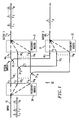
- FIG. 1 is a diagram of an example of an optical tunable channel dropping filter in accordance with this invention.
- FIGS. 2(a) and 2(b) are diagrams of the frequency routing devices employed in the optical channel dropping filter of this invention.
- FIG. 3 is a diagram of an alternative example of an optical tunable channel dropping filter in accordance with this invention.
- FIG. 4 is a diagram illustrating the details of the frequency routing devices shown in FIG. 2.
- FIG. 1 shows an example of the tunable channel dropping filter of the present invention. It is composed of three frequency routing devices 30, 31 and 32 coupled by waveguides and optical switches. These structures may be monolithically integrated on a semiconductive wafer. They may be created by known photolithographic techniques.
- the frequency routing devices employed in the present invention operate as multiplexers and demultiplexers of optical frequencies. The details of their construction and operation are more fully described in U.S. Patent Nos. 5,002,350 and 5,136,671 to Dragone, the entire contents of which are hereby incorporated by reference into this application. Before the tunable filter of the present invention is described, the pertinent features of the frequency routing devices will be reviewed.
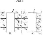
- FIGS. 2(a) and (b) show a functional illustration of a routing device 12 of the type employed in the present invention.
- the routing device may have N input waveguides and M output waveguides to form an NxM frequency routing device.
- the routing device 12 shown in Fig. 1(a) has four input waveguides 161, 162, 163, 164 and four output waveguides 181 182, 183, 184.
- the output waveguide to which a particular frequency component will be directed is a function of the frequency and the particular input waveguide to which the frequency component is directed.
- the routing device 12 can be configured to demultiplex preselected input optical frequencies directed to any of its input waveguides. For example, as seen in FIG.
- frequency F1 will be directed to output waveguide 181
- frequency F2 will be directed to output waveguide 182
- frequency F3 will be directed to output waveguide 183
- frequency F4 will be directed to output waveguide 184.
- FIG. 2(b) illustrates the manner in which the optical signal is demultiplexed by the frequency routing device seen in FIG. 2(a) if it is directed to the second input waveguide 162 rather than the first input waveguide 161.
- frequency F1 will be directed to output waveguide 182
- frequency F2 will be directed to output waveguide 183
- frequency F3 will be directed to output waveguide 184
- frequency F4 will be directed back up to output waveguide 181 since the routing device 12 only has four output waveguides.
- the routing device 12 is provided with a fifth output waveguide 185 (shown in dashed lines in FIG. 2(b) ) to form a 4x5 routing device, frequency F4 will appear on this fifth output waveguide instead of on the first output waveguide 181.
- routing devices discussed above are symmetrical in operation. For example, assuming the routing device shown in FIG. 2(a) is a 5x5 routing device, if frequencies F1, F2, F3, F4 are directed to waveguides 181, 182, 184 and 185, respectively (which now function as input waveguides), frequencies F1 and F2 will be output on waveguide 161 and frequencies F3 and F4 will be output on waveguide 162.
- FIGS. 1 and 2 A general property of the frequency routing device seen in FIG. 2, which is configured to demultiplex and multiplex a given set of frequency components, is suggested by FIGS. 1 and 2. Specifically, if an optical signal is directed to any selected input waveguide 16 i , the first frequency component of the signal will appear on output waveguide 181. Subsequent frequency components will appear on the successive output waveguides (i.e., the second frequency component will appear on output waveguide 18 (i+1) , the third frequency component will appear on output waveguide 18 (i+2) , etc.).
- the tunable channel dropping filter 35 of the present invention is composed of three frequency routing devices 30, 31 and 32.
- the first routing device 30 in which the input signal is directed is a 1xN routing device, where N is the number of frequencies contained in the multiplexed input signal.
- the second and third routing devices 31 and 32 are each Nx1 routing devices.
- the N output waveguides 181,182, ..., 18 N of the first routing device 30 are each coupled to an optical switch 211, 212, ..., 21 N , respectively.
- Each optical switch has two outputs.
- the first output of the switches 211, 212, ..., 21 N are connected to the inputs 161, 162, ..., 16 N , respectively, of the second routing device 31.
- the second output of the switches 211, 212, ..., 21 N are connected to the inputs 161, 162, ..., respectively, of the third routing device 32.
- the first output is coupled to input waveguide 16 i of the second routing device 31 and its second output is coupled to input waveguide 16 i of the third routing device 32.
- the signal that is input to the optical switch from the first routing device 30 will be ultimately directed to the output of either the second routing device 31 or the third routing device 32 based on the state of the switch.
- Such optical switches and the corresponding control means are known devices and hence will not be discussed further.
- the tunable channel dropping filter 35 operates as follows.
- a multiplexed signal composed of frequencies F1, F2, ... F N is input to the first frequency routing device 30.
- the first routing device 30 demultiplexes the input signal so that each frequency F i is directed to output waveguide 18 i .
- each frequency F i will be directed to the input waveguide 16 i of either the second or third routing device 31 or 32.
- optical switch 21 i is in a first state
- frequency F i will be directed to input waveguide 16 i of the second routing device 31.
- frequency F i will be directed to input waveguide 16 i of the third routing device 32.
- Those individual frequencies F i which are directed to the corresponding inputs 16 i of the second routing device 31 will be multiplexed so that a single multiplexed signal is directed to the output waveguide 181 of the second routing device 31.
- those individual frequencies F j which are directed to the corresponding inputs 16 j of the third routing device 32 will be multiplexed so that a single multiplexed signal is directed to the output waveguide 181 of the third routing device 32.
- a multiplexed signal directed to the input of the filter 35 has its individual frequency components directed to one of two output waveguides in accordance with the state of the optical switch through which each frequency component must pass.
- Each optical switch 211, 222, ..., 22 N can be switched between states independently of the remaining optical switches by employing appropriate control means. As a result, the frequency components of the optical input signal can be divided between the two output waveguides in any manner desired.
- optical switches 211, 213, .... and 21 N are in a first state so that frequencies F1, F3, ..., F N are directed as a multiplexed signal to the output waveguide 181 of the second routing device 31.
- Optical switch 212 is in a second state and thus frequency F2 is directed to the output waveguide 181 of the third routing device 32.
- the multiplexed output signal directed to output waveguide 181 of the second frequency routing device 31 corresponds to the input signal except that one frequency or channel (i.e., frequency F2) has been dropped from the signal.
- FIG 3 shows an alternative example of the invention which requires only two frequency routing devices but which employs both optical switches and optical couplers.
- these components may be all monolithically integrated on a single semiconductive wafer.
- the first routing device 230 is a 1x(N-1) routing device and the second routing device 231 is an Nx2 routing device.
- N the number of routing devices
- the output waveguides 2181, 2182, ..., 218 (N-1) of the first routing device 230 are connected to the optical switches 2211, 2212, ..., 221 (N-1) , respectively.
- the first output 218 i of each optical switch 221 i is connected to the input waveguide 216 i of the second routing device 231 via an optical coupler 237 i such as a 3dB optical coupler which is inserted in series with the input waveguide 216 i .
- the second output of each optical switch 221 i is connected to the input waveguide 216 (i+1) of the second routing device 231 via the optical coupler 237 (i+1) that is in series with the input waveguide 216 (i+1) .
- each output waveguide of the first routing device is coupled in consecutive order to the corresponding input of the second routing device via the first output of the optical switch in series therewith.
- Each output waveguide of the first routing device is also coupled in consecutive order to the subsequent or adjacent input of the second routing device via the second output of the optical switch in series therewith.
- the example of the tunable channel dropping filter 235 shown in FIG. 3 operates as follows.
- the multiplexed signal composed of frequencies F1, F2, ..., F (N-1) is demultiplexed by the first frequency routing device 230 so that each F i is directed to output waveguide 218 j .
- each frequency F i will be directed to either input waveguide 216 i or adjacent input waveguide 216 (i+1) of the second routing device 231 through the optical couplers.
- frequency F i will be directed to input waveguide 216 i of the second routing device 231.
- frequency F i will be directed to input waveguide 216 (i+1) of the second routing device 231.
- Those individual frequencies F i which are directed to the corresponding inputs 216 i of the second routing device 231 will be multiplexed by the second routing device 231 so that a single multiplexed signal is directed to the first output waveguide 2181 of the second routing device 231.
- those individual frequencies F j appearing on output waveguides 218 j of the first routing device 230 which are directed to the adjacent inputs 216 (j+1) of the second routing device 231 will be multiplexed by the second routing device 231 so that a single multiplexed signal is directed to the second output waveguide 2182 of the second routing device 231.
- a multiplexed signal directed to the input of the filter 235 shown in FIG. 3 has its individual frequency components directed to one of two output waveguides in accordance with the state of the optical switch through which each frequency component must pass.
- optical switches 2211, 2213,... 221 (N-2) are all shown in a first state so that frequencies F1, F3, ..., F (N-2) are directed as a multiplexed signal to the output waveguide 2181 of the second routing device 231.
- Optical switches 2212 and 221 (N-1) are in a second state and thus frequencies F2 and F (N-1) are directed to the output waveguide 2182 of the second routing device 231.
- the multiplexed output signal directed to output waveguide 2181 of the second frequency routing device 231 corresponds to the input signal except that two frequencies or channels (i.e., frequencies F2 and F (N-1) ) have been dropped from the signal.
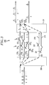
- FIG. 4 shows the pertinent details of the frequency routing devices employed in the invention. All of these devices may have identical configurations except for, possibly, the differing numbers of input and output waveguides that are employed.
- Each frequency routing device contains a plurality of input waveguides 26 connected to a free space region 28.
- a plurality of output waveguides 40 extends from the free space region 28 and is connected to an optical grading 42.
- the optical grading 42 comprises a plurality of unequal length waveguides which provides a predetermined amount of path length difference to a corresponding plurality of input waveguides 44 connected to another free space region 46.
- the free space region 46 is connected to a plurality of output waveguides 38.
- These frequency routing devices operate as multiplexers and demultiplexers of optical frequencies.
- the input waveguide 16 corresponds to one of the input waveguides 26 shown in FIG. 4.
- the output waveguide 181 corresponds to one of the output waveguides 38 shown in FIG. 4.
- the output waveguide 181 corresponds to one of the output waveguides 38 shown in FIG. 4.
- The.example of the filter shown in FIG. 3 employs the frequency routing device shown in FIG. 4 in a manner similar to that discussed in connection with the filter shown in FIG. 1.
Landscapes
- Physics & Mathematics (AREA)
- General Physics & Mathematics (AREA)
- Optics & Photonics (AREA)
- Engineering & Computer Science (AREA)
- Computer Networks & Wireless Communication (AREA)
- Microelectronics & Electronic Packaging (AREA)
- Signal Processing (AREA)
- Optical Communication System (AREA)
- Optical Integrated Circuits (AREA)
Applications Claiming Priority (2)
| Application Number | Priority Date | Filing Date | Title |
|---|---|---|---|
| US08/153,523 US5493625A (en) | 1993-11-16 | 1993-11-16 | Fast tunable channel dropping filter |
| US153523 | 1993-11-16 |
Publications (2)
| Publication Number | Publication Date |
|---|---|
| EP0655874A2 true EP0655874A2 (de) | 1995-05-31 |
| EP0655874A3 EP0655874A3 (de) | 1996-02-21 |
Family
ID=22547575
Family Applications (1)
| Application Number | Title | Priority Date | Filing Date |
|---|---|---|---|
| EP94308237A Withdrawn EP0655874A3 (de) | 1993-11-16 | 1994-11-09 | Schnelles abstimmbares Kanalentnahmefilter. |
Country Status (6)
| Country | Link |
|---|---|
| US (1) | US5493625A (de) |
| EP (1) | EP0655874A3 (de) |
| JP (1) | JPH07202802A (de) |
| KR (1) | KR950016058A (de) |
| AU (1) | AU7774594A (de) |
| CA (1) | CA2130789C (de) |
Cited By (5)
| Publication number | Priority date | Publication date | Assignee | Title |
|---|---|---|---|---|
| FR2752119A1 (fr) * | 1996-07-31 | 1998-02-06 | Kokusai Denshin Denwa Co Ltd | Equipement optique de connexion croisee et equipement d'addition/de supression de signaux incluant un tel equipement optique de connexion croisee |
| EP0720408A3 (de) * | 1994-12-28 | 1999-08-18 | AT&T Corp. | Abstimmbarer optischer Einfüge-/Abzweigfilter für beliebige Kanalanordnungen |
| EP0932060A3 (de) * | 1998-01-27 | 2001-04-18 | Agilent Technologies, Inc. | Wählbares Wellenlängenkanalfilter für optische WDM Systeme |
| FR2821504A1 (fr) * | 2001-02-23 | 2002-08-30 | Cit Alcatel | Dispositif d'extraction de frequence |
| US20220385373A1 (en) * | 2021-05-28 | 2022-12-01 | Fujitsu Limited | Wavelength converter, optical communication apparatus, and optical waveguide substrate |
Families Citing this family (24)
| Publication number | Priority date | Publication date | Assignee | Title |
|---|---|---|---|---|
| US6233077B1 (en) | 1995-05-11 | 2001-05-15 | Ciena Corporation | Remodulating channel selectors for WDM optical communication systems |
| US9191117B2 (en) * | 1995-05-11 | 2015-11-17 | Ciena Corporation | High-speed optical transponder systems |
| US5715076A (en) * | 1995-05-11 | 1998-02-03 | Ciena Corporation | Remodulating channel selectors for WDM optical communication systems |
| JP3006670B2 (ja) * | 1995-08-18 | 2000-02-07 | 日本電気株式会社 | 光海底分岐装置およびその伝送路切替方法 |
| US6097517A (en) * | 1995-09-01 | 2000-08-01 | Oki Electric Industry Co., Ltd. | Wavelength router |
| US5680490A (en) * | 1995-09-08 | 1997-10-21 | Lucent Technologies Inc. | Comb splitting system and method for a multichannel optical fiber communication network |
| US5710846A (en) * | 1996-03-26 | 1998-01-20 | Rf Systems, Inc. | Self-calibrating optical fiber switch |
| JPH1093164A (ja) * | 1996-09-17 | 1998-04-10 | Kokusai Denshin Denwa Co Ltd <Kdd> | 多波長光源及び離散波長可変光源 |
| US5742414A (en) * | 1996-09-24 | 1998-04-21 | At&T Corp. | Multiplicity of services via a wavelength division router |
| US5953141A (en) * | 1996-10-03 | 1999-09-14 | International Business Machines Corporation | Dynamic optical add-drop multiplexers and wavelength-routing networks with improved survivability and minimized spectral filtering |
| US6271949B1 (en) * | 1996-12-18 | 2001-08-07 | Nec Corporation | Optical communication system using wavelength-division multiplexed light |
| US6724995B1 (en) | 1996-12-23 | 2004-04-20 | Tellabs Denmark A/S | Bidirectional router and a method of bidirectional amplification |
| US5940556A (en) * | 1997-03-07 | 1999-08-17 | Ifos | Fiber-optic mode-routed add-drop filter |
| WO1998049587A1 (en) * | 1997-05-01 | 1998-11-05 | Trustees Of The Stevens Institute Of Technology | Method and apparatus for modulation of guided plasmons |
| US6005995A (en) * | 1997-08-01 | 1999-12-21 | Dicon Fiberoptics, Inc. | Frequency sorter, and frequency locker for monitoring frequency shift of radiation source |
| US6301031B2 (en) * | 1997-09-02 | 2001-10-09 | Agere Systems Optoelectronics Guardian Corp. | Method and apparatus for wavelength-channel tracking and alignment within an optical communications system |
| US6285477B1 (en) * | 1997-09-17 | 2001-09-04 | Kokusai Denshin Denwa Kabushiki Kaisha | Multi-wavelength light source and discrete-wavelength-variable light source |
| US6400478B1 (en) | 1998-04-02 | 2002-06-04 | Sorrento Networks, Inc. | Wavelength-division-multiplexed optical transmission system with expanded bidirectional transmission capacity over a single fiber |
| US6091869A (en) * | 1998-04-30 | 2000-07-18 | Telefonaktiebolaget Lm Ericsson | Low loss, optical add/drop WDM node |
| US6263125B1 (en) * | 1998-05-19 | 2001-07-17 | Lynx Photonic Networks Inc | Integrated optical switch array |
| US6782203B2 (en) * | 1998-08-31 | 2004-08-24 | Lucent Technologies Inc. | Scalable optical demultiplexing arrangement for wide band dense wavelength division multiplexed systems |
| US6721508B1 (en) | 1998-12-14 | 2004-04-13 | Tellabs Operations Inc. | Optical line terminal arrangement, apparatus and methods |
| US6498682B2 (en) | 1998-12-28 | 2002-12-24 | At&T Corp. | Tunable add/drop filter |
| US20030020926A1 (en) * | 2001-05-15 | 2003-01-30 | Nicolae Miron | Tunable band pass optical filter unit with a tunable band pass interferometer |
Family Cites Families (9)
| Publication number | Priority date | Publication date | Assignee | Title |
|---|---|---|---|---|
| US4673270A (en) * | 1985-06-28 | 1987-06-16 | Amp Incorporated | Channel add/drop filter-coupler |
| US4890893A (en) * | 1989-03-02 | 1990-01-02 | Bell Communications Research, Inc. | Dark fiber switched bandwidth filter |
| JP2692316B2 (ja) * | 1989-11-20 | 1997-12-17 | 日本電気株式会社 | 波長分割光交換機 |
| US5002350A (en) * | 1990-02-26 | 1991-03-26 | At&T Bell Laboratories | Optical multiplexer/demultiplexer |
| US5093876A (en) * | 1990-07-27 | 1992-03-03 | At&T Bell Laboratories | WDM systems incorporating adiabatic reflection filters |
| US5136671A (en) * | 1991-08-21 | 1992-08-04 | At&T Bell Laboratories | Optical switch, multiplexer, and demultiplexer |
| US5233453A (en) * | 1992-04-29 | 1993-08-03 | International Business Machines Corporation | Space-division switched waveguide array filter and method using same |
| US5339157A (en) * | 1993-02-19 | 1994-08-16 | At&T Bell Laboratories | Rapidly tunable integrated optical filter |
| US5309534A (en) * | 1993-02-24 | 1994-05-03 | At&T Bell Laboratories | Optical filter having multiple interferometric stages |
-
1993
- 1993-11-16 US US08/153,523 patent/US5493625A/en not_active Expired - Lifetime
-
1994
- 1994-08-24 CA CA002130789A patent/CA2130789C/en not_active Expired - Fee Related
- 1994-11-07 KR KR1019940029024A patent/KR950016058A/ko not_active Ceased
- 1994-11-09 AU AU77745/94A patent/AU7774594A/en not_active Abandoned
- 1994-11-09 EP EP94308237A patent/EP0655874A3/de not_active Withdrawn
- 1994-11-16 JP JP6305709A patent/JPH07202802A/ja active Pending
Cited By (7)
| Publication number | Priority date | Publication date | Assignee | Title |
|---|---|---|---|---|
| EP0720408A3 (de) * | 1994-12-28 | 1999-08-18 | AT&T Corp. | Abstimmbarer optischer Einfüge-/Abzweigfilter für beliebige Kanalanordnungen |
| FR2752119A1 (fr) * | 1996-07-31 | 1998-02-06 | Kokusai Denshin Denwa Co Ltd | Equipement optique de connexion croisee et equipement d'addition/de supression de signaux incluant un tel equipement optique de connexion croisee |
| EP0932060A3 (de) * | 1998-01-27 | 2001-04-18 | Agilent Technologies, Inc. | Wählbares Wellenlängenkanalfilter für optische WDM Systeme |
| FR2821504A1 (fr) * | 2001-02-23 | 2002-08-30 | Cit Alcatel | Dispositif d'extraction de frequence |
| US7058302B2 (en) | 2001-02-23 | 2006-06-06 | Alcatel | Frequency extractor |
| EP1235377A3 (de) * | 2001-02-23 | 2008-11-12 | Alcatel Lucent | Vorrichtung zum Frequenz Abführen |
| US20220385373A1 (en) * | 2021-05-28 | 2022-12-01 | Fujitsu Limited | Wavelength converter, optical communication apparatus, and optical waveguide substrate |
Also Published As
| Publication number | Publication date |
|---|---|
| JPH07202802A (ja) | 1995-08-04 |
| CA2130789A1 (en) | 1995-05-17 |
| US5493625A (en) | 1996-02-20 |
| KR950016058A (ko) | 1995-06-17 |
| EP0655874A3 (de) | 1996-02-21 |
| CA2130789C (en) | 1998-09-22 |
| AU7774594A (en) | 1995-05-25 |
Similar Documents
| Publication | Publication Date | Title |
|---|---|---|
| EP0655874A2 (de) | Schnelles abstimmbares Kanalentnahmefilter | |
| US5339157A (en) | Rapidly tunable integrated optical filter | |
| EP0649040B1 (de) | Optischer Bandpass-Filter | |
| US5542010A (en) | Rapidly tunable wideband integrated optical filter | |
| US5493434A (en) | Photonic frequency division multiplexed FIFO buffer | |
| US5526153A (en) | Optical channel adding/dropping filter | |
| CA2163059C (en) | Tunable add/drop optical filter providing arbitrary channel arrangements | |
| EP0702253A2 (de) | Frequenzablenkungsvorrichtung mit breitem und im wesentlichen flachen Durchlassband | |
| JP3705710B2 (ja) | 光クロスコネクト装置及びスイッチング装置 | |
| EP0726691A2 (de) | Kombinierter Wellenlängenrouter und Vermittlungseinrichtung für ein optisches Wellenlängenmultiplex-Kommunikationssystem | |
| JP3448182B2 (ja) | 全光ファイバ製光ルータ | |
| JP4388681B2 (ja) | 追加/ドロップ光多重化装置とチャンネルを付加する方法 | |
| EP1116346B1 (de) | Abstimmbarer einfüge-/ausblendmultiplexer | |
| US6782156B2 (en) | Interleaved band demultiplexing/multiplexing system | |
| SE518532C2 (sv) | Våglängdsselektiv anordning respektive väljare samt förfarande därvid | |
| US6292605B1 (en) | Reconfigurable optical filtering apparatus and a drop-and-insert multiplexer incorporating such apparatus | |
| US20020186431A1 (en) | Method of organizing wavelength channels in a wavelength-division multiplexed network as well as an optical wavelength-division multiplexed network, optical hub, optical add/drop multiplexer and optical filter bank therefor | |
| JPH0846569A (ja) | 周波数チャネル選択フィルタ | |
| JPH0349238B2 (de) | ||
| JPH01187537A (ja) | 波長変換スイッチ | |
| JP2000188571A (ja) | 波長多重光切換装置 |
Legal Events
| Date | Code | Title | Description |
|---|---|---|---|
| PUAI | Public reference made under article 153(3) epc to a published international application that has entered the european phase |
Free format text: ORIGINAL CODE: 0009012 |
|
| AK | Designated contracting states |
Kind code of ref document: A2 Designated state(s): DE FR GB IT NL SE |
|
| PUAL | Search report despatched |
Free format text: ORIGINAL CODE: 0009013 |
|
| AK | Designated contracting states |
Kind code of ref document: A3 Designated state(s): DE FR GB IT NL SE |
|
| 17P | Request for examination filed |
Effective date: 19960812 |
|
| STAA | Information on the status of an ep patent application or granted ep patent |
Free format text: STATUS: THE APPLICATION HAS BEEN WITHDRAWN |
|
| 18W | Application withdrawn |
Withdrawal date: 20010124 |