EP0654875A1 - Elektronische Simulation zur Kompensation von Wärmeeffekten in Diodenlaser - Google Patents
Elektronische Simulation zur Kompensation von Wärmeeffekten in Diodenlaser Download PDFInfo
- Publication number
- EP0654875A1 EP0654875A1 EP94308554A EP94308554A EP0654875A1 EP 0654875 A1 EP0654875 A1 EP 0654875A1 EP 94308554 A EP94308554 A EP 94308554A EP 94308554 A EP94308554 A EP 94308554A EP 0654875 A1 EP0654875 A1 EP 0654875A1
- Authority
- EP
- European Patent Office
- Prior art keywords
- laser
- signal
- resistor
- circuit
- control signal
- Prior art date
- Legal status (The legal status is an assumption and is not a legal conclusion. Google has not performed a legal analysis and makes no representation as to the accuracy of the status listed.)
- Granted
Links
- 230000000694 effects Effects 0.000 title claims abstract description 78
- 238000004088 simulation Methods 0.000 title abstract description 15
- 239000003990 capacitor Substances 0.000 claims abstract description 18
- 238000012937 correction Methods 0.000 abstract description 32
- 238000010438 heat treatment Methods 0.000 description 15
- 230000008859 change Effects 0.000 description 5
- 238000000034 method Methods 0.000 description 5
- 230000000630 rising effect Effects 0.000 description 5
- 230000000712 assembly Effects 0.000 description 4
- 238000000429 assembly Methods 0.000 description 4
- 108091008695 photoreceptors Proteins 0.000 description 4
- 238000010586 diagram Methods 0.000 description 3
- 230000004913 activation Effects 0.000 description 2
- 230000032683 aging Effects 0.000 description 1
- 230000003679 aging effect Effects 0.000 description 1
- 238000013459 approach Methods 0.000 description 1
- 230000002457 bidirectional effect Effects 0.000 description 1
- 238000001816 cooling Methods 0.000 description 1
- 230000007423 decrease Effects 0.000 description 1
- 230000001419 dependent effect Effects 0.000 description 1
- 238000013461 design Methods 0.000 description 1
- 230000009977 dual effect Effects 0.000 description 1
- 230000004907 flux Effects 0.000 description 1
- 238000004093 laser heating Methods 0.000 description 1
- 230000007774 longterm Effects 0.000 description 1
- 238000012986 modification Methods 0.000 description 1
- 230000004048 modification Effects 0.000 description 1
- 230000002250 progressing effect Effects 0.000 description 1
- 230000035945 sensitivity Effects 0.000 description 1
- 239000000758 substrate Substances 0.000 description 1
Images


Classifications
-
- H—ELECTRICITY
- H01—ELECTRIC ELEMENTS
- H01S—DEVICES USING THE PROCESS OF LIGHT AMPLIFICATION BY STIMULATED EMISSION OF RADIATION [LASER] TO AMPLIFY OR GENERATE LIGHT; DEVICES USING STIMULATED EMISSION OF ELECTROMAGNETIC RADIATION IN WAVE RANGES OTHER THAN OPTICAL
- H01S5/00—Semiconductor lasers
- H01S5/06—Arrangements for controlling the laser output parameters, e.g. by operating on the active medium
- H01S5/062—Arrangements for controlling the laser output parameters, e.g. by operating on the active medium by varying the potential of the electrodes
- H01S5/06209—Arrangements for controlling the laser output parameters, e.g. by operating on the active medium by varying the potential of the electrodes in single-section lasers
- H01S5/06216—Pulse modulation or generation
-
- H—ELECTRICITY
- H01—ELECTRIC ELEMENTS
- H01S—DEVICES USING THE PROCESS OF LIGHT AMPLIFICATION BY STIMULATED EMISSION OF RADIATION [LASER] TO AMPLIFY OR GENERATE LIGHT; DEVICES USING STIMULATED EMISSION OF ELECTROMAGNETIC RADIATION IN WAVE RANGES OTHER THAN OPTICAL
- H01S5/00—Semiconductor lasers
- H01S5/06—Arrangements for controlling the laser output parameters, e.g. by operating on the active medium
- H01S5/068—Stabilisation of laser output parameters
-
- H—ELECTRICITY
- H01—ELECTRIC ELEMENTS
- H01S—DEVICES USING THE PROCESS OF LIGHT AMPLIFICATION BY STIMULATED EMISSION OF RADIATION [LASER] TO AMPLIFY OR GENERATE LIGHT; DEVICES USING STIMULATED EMISSION OF ELECTROMAGNETIC RADIATION IN WAVE RANGES OTHER THAN OPTICAL
- H01S5/00—Semiconductor lasers
- H01S5/40—Arrangement of two or more semiconductor lasers, not provided for in groups H01S5/02 - H01S5/30
- H01S5/4025—Array arrangements, e.g. constituted by discrete laser diodes or laser bar
Definitions
- This invention relates generally to laser diodes and more particularly concerns an electronic simulation in which thermal effects are modeled and used for correcting laser diode output.
- a single beam laser diode assembly has a single diode and usually, in a scanning system, the diode is driven by a train of image pixel information.
- the pixel information is used to drive the diode and therefore stimulate laser flux emission where there is a white pixel in a write white system.
- a laser is turned on to create white space on a page. Intensity of the light beam is directly proportional to the output power of the laser.
- the temperature of the diode should be kept at a constant level.
- the temperature of the diode fluctuates, which in turn causes the output power of the diode and the intensity of the light beam to fluctuate.
- a multiple beam diode assembly has at least two diodes in close proximity on a common substrate. Each diode is driven by a separate train of image pixel information. Again, as the pixels change, the temperature of each diode fluctuates. However, in a multiple diode system, the changing temperature of a diode also causes a temperature fluctuation in adjacent diodes. The temperature fluctuations of the adjacent diodes cause the output power and the intensity of the light beams in those adjacent diodes also to fluctuate.
- a tri-level system may use one or more diodes with at least one diode operating at full on, full off, and partially on.
- One example of an application using a single diode tri-level system is the printing of black and white documents with a highlight color. Tri-level systems suffer from the same heating effects both in the full on and the partially on modes of the laser.
- the intensity variation in a diode over time is shown due to heating and cooling effects.
- a first laser beam 10 is left turned on while a second laser beam 12 from an adjacent laser is cycled from a full on position to a full off position using a step function. While the second laser beam 12 is on, heating effects on the first beam 10 cause the intensity to drift downward and finally stabilize at a lower value.
- the change in intensity is the drift d c .
- a similar curve is produced from self-heating effects in the second laser 12 when it is turned on. The self-heating effects are seen in the falling time constant t fs .
- the rising time constant t rc or the falling time constant t fc when compared to falling time constant t fs , produced from self-heating, is larger.
- the difference in the output intensity is the drift d s
- the drift d c is smaller than the drift d s .
- the intensity of the first beam 10 drifts upward and stabilizes at a higher value.
- the amount the intensity changes is the intensity drift d c .
- the amount of time needed for the intensity to drift and stabilize is a rising time constant t rc .
- rising time constant t rc and falling time constant t fc are nearly the same. This is important in designing a simulator since both the rising time constant t rc and falling time constant t fc can then be adequately modeled using a single circuit for both. A more accurate but more complicated circuit could be built to model the rising time constant t rc and the falling time constant t fc independently of each other.
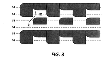
- FIG 2 shows the half tone pattern when it is correctly printed with no heating effects.
- Scan lines s1 and s5 are all black.
- Scan lines s2, s3, and s6 are alternating blocks of black and white.
- Scan line s4 is all white.
- the laser is turned on to create white space and turned off to create black space.
- Rectangle R1 is the first white rectangle printed on scan line s2.
- Figure 3 is the pattern shown in Figure 2 when it is printed with a single laser diode experiencing self-heating effects.
- a laser remains off the entire time since the entire line is black.
- the laser starts scanning in the off position but shortly turns on when it enters rectangle R1.
- the spot intensity is at its peak and gradually diminishes and stabilizes as shown in Figure 1.
- the resulting change in spot size from large to small will create sloping edges E on rectangle R1. Every time the laser turns on, the same sloping edges E will be produced until the intensity and spot size stabilize.
- One method for compensating for laser drift would be to use a direct, real time feedback system.
- direct feedback systems have the disadvantages of being very expensive to construct, requiring extremely fast components to effectively calculate and provide a real time corrective signal, and requiring additional light paths in the printing system. Therefore, some other method must be found.
- the present invention uses the idea that laser drift can be modeled accurately enough to generate an appropriate correction signal.
- the laser drift can be computed using the model.
- the correction of the laser drift can then be implemented and presented to the model to observe the correction effects.
- the important requirement is to make a model which faithfully models the physics of the actual heating effects of the laser.
- a compensation method based on a simulation of the laser heating effects has the advantages of being inexpensive and reliable while requiring no additional light paths and being easy to install and adapt to many different printing systems.
- video data input signal 20 on line 22 is applied to a thermal effects simulator 24.
- the automatic gain control signal 30 on line 32 adjusts to control the light laser 40 due to long term effects such as aging of the photoreceptor.
- the video data input signal 20 is used to activate a switch which turns a laser 40 on or off according to the desired printed pattern.
- the video data input signal 20 becomes positive corresponding to white space on a printed page and the laser 40 is turned on .
- the thermal effects simulator 24 responds to the video data input signal 20 and the automatic gain control signal 30 by outputting a signal linearly proportional to the automatic gain control signal 30 when modulated by the effects of simulated temperature rise.
- the new signal transmitted by the thermal effects simulator 24 is the thermal effects correction signal 26 on line 28 and is used to compensate for thermal droop effects.
- the thermal effects correction signal 26 and the automatic gain control signal 30 on line 32 are both applied to an adder 34.
- the automatic gain control signal 30 is determined by photoreceptor sensitivity and other system factors. Since, over time, the photoreceptor becomes less sensitive, the signal must be increased to increase the laser 40 output.
- a laser control signal 36 on line 38 is emitted by an adder 34 to be applied to laser 40.
- the laser control signal 36 contains both the thermal effects correction signal 26, to correct for thermal effects, and the automatic gain control signal 30, to correct for photoreceptor aging effects.
- the thermal effects simulator 24 contains circuitry which appropriately simulates laser droop and generates a correction signal.
- the simlator is programmed or implemented with a standard time constant. Using the falling time constant t fs , the thermal effects simulator 24 can compensate for the drift d s in intensity (as shown in Figure 1) by increasing the thermal effects correction signal 26. The increased thermal effects correction signal 26 will cause an increase in intensity of the laser.
- the circuit in Figure 4 applies a first order corrective increase in the current to compensate for a downward drift in laser intensity.
- the laser will respond to the increased current by increasing its ouput, which will also generate more heat causing additional thermal effects.
- a circuit shown in Figure 5, can be used to compensate for higher order thermal effects.
- the laser control signal 36 is applied to the thermal effects simulator 24 rather than the automatic gain control signal 30.
- the thermal effects correction signal 26 is equal to zero.
- the thermal effects simulator 24 responds, the thermal effects correction signal 26 rises and is added to the automatic gain control signal 30 to form the laser control signal 36.
- the laser control signal 36 rises, it is fed back to the thermal effects simulator 24 which can then increase the thermal effects correction signal 26 further to compensate for the additional thermal effects.
- the circuitry inside the thermal effects simulator 24, shown in Figures 4-5, is shown in Figure 6.
- the video data input signal 20 on line 22 is connected directly to a two pole switch S that switches between the laser control signal 36 on line 38 or the automatic gain control signal 30 on line 32 and ground 42.
- the two pole switch S is shown connected to ground 42.
- the thermal effects correction signal 26 and one side of a capacitor 46 are then connected to ground 42 through the resistor 44. The other side of the capacitor 46 is always connected to ground 48.
- the thermal effects correction signal 26 is zero since it is pulled to ground 42.
- FIG 7 shows the identical circuit with the two pole switch S connected to the laser control signal 36. This happens when the video data input signal 20 goes high (in our write white system).
- the thermal effects correction signal 26 is now connected to the laser control signal 36 through the RC circuit consisting of the resistor 44 and the capacitor 46.
- the values of the resistor 44 and the capacitor 46 are chosen to produce a time constant for the RC circuit that is equivalent to the falling time constant t fs shown in Figure 1. As the capacitor 46 charges, a small signal that is proportional to the laser control signal 36 on line 38, appears on line 28.
- thermal effects correction signal 26 shown in Figure 8 There are many ways, known in the art, to create the thermal effects correction signal 26 shown in Figure 8.
- the RC circuit could be replaced with an equivalent RL circuit, multiple RC or RL circuits, or any combination thereof, as known in the art.
- the signal could be approximated digitally, using a miroprocessor, ROM, RAM, or other digital circuit, as known in the art, as shown in Figure 9.
- the ideal thermal effects correction signal 26 is shown as a fine dotted line while the actual thermal effects correction signal 26 is shown as a solid line.
- the resistor 44 has been replaced with a variable resistor 44. Since this resistor 44 sets the value of the time constant of the RC circuit to be equal to the time constant t fs of the circuit, changing this resistor provides adjustability in the RC circuit.
- a variable resistor 50 has been connected to the two pole switch S between the two pole switch S and the resistor 44 at node 45.
- the other end of the resistor 50 is shown connected to a voltage source 52.
- the resistor 50 affects the offset adjustment of the thermal effects correction signal 26. By changing the value of the resistor 50 the offset adjustment can be set.
- Resistor 51 has been added between to receive laser control signal 36 prior to two pole switch S to insure correct operation of resistor 50 to provide a voltage change at node 45 when it is adjusted. Offset adjustment is used since laser output is not directly proportional to laser input current. The offset adjustment then adds an appropriate amount of current to achieve the desired laser output.
- variable resistor 54 is shown connected between the thermal effects correction signal 26 on line 28 and the junction between resistor 44 and capacitor 46.
- Variable resistor 54 is bidirectionally connected to the adder 34 through the thermal effects correction signal 26 on line 28.
- the other end of the variable resistor 54 is connected to ground 56.
- the resistor 54 affects the scaling factor used to create the thermal effects correction signal 26. By changing the value of the resistor 50 the scaling factor can be adjusted.
- the two pole switch S may be implemented using a multiplier, and outputs should be adequately buffered to avoid an undue load on individual points in the circuit.
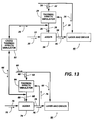
- FIG. 13 a circuit to compensate for cross heating effects is shown.
- the thermal effects simulators 24, 64 of two adjacent laser systems are bidirectionally connected to a third cross thermal effects simulator 82, designed to compensate for cross thermal effects, through the thermal effects correction signals 26, 66.
- Each laser system is comprised of a video data input signal 20, 60 which is fed to its respective thermal effects simulator 24, 64 on line 22, 62 and a laser and driver assembly 40,80.
- the thermal effects simulators 24, 64 also receive input from its respective laser control signals 36, 76 on lines 38, 78.
- the thermal effects simulators 24, 64 then produce thermal effects correction signals 26, 66 on lines 28, 68 which is sent to adders 34, 74 to be combined with automatic gain control signals 30, 70 in adders 34,74.
- the adders 34,74 produce laser control signals 36, 76 which controls the lasers in the laser and driver assemblies 40, 80, respectively.
- the resultant correction current will have the same shape as the curve shown in Figure 8.
- Figure 14 illustrates a simple version of the circuit inside the thermal effects simulator 82.
- Two series resistors 84, 86 are connected to the bidirectional outputs of the thermal effects simulator 82.
- a capacitor 88 is connected to ground 90 on one end and between the two series resistors 84, 86 on the other end.
- Resistor 86 is used to set a time constant for one assembly and resistor 84 is used to set a time constant for the other assembly. Since both resistors 84, 86 are variable resistors then the time constants can be adjusted by varying the resistance.
- Figure 15 shows a variation of Figure 14.
- Resistor 92 is added between capacitor 88 and the junction of resistor 86 and resistor 84 to provide better tunability of time constants.
- thermal effects correction signal 26 shown in Figure 14 there are many ways, known in the art, to create the thermal effects correction signal 26 shown in Figure 14.
- the RC circuit could be replaced with an equivalent LC circuit, as known in the art, or the signal could be approximated digitally, using a miroprocessor, ROM, RAM, or other digital circuit, as known in the art.
Landscapes
- Physics & Mathematics (AREA)
- Condensed Matter Physics & Semiconductors (AREA)
- General Physics & Mathematics (AREA)
- Electromagnetism (AREA)
- Optics & Photonics (AREA)
- Semiconductor Lasers (AREA)
- Laser Beam Printer (AREA)
Applications Claiming Priority (2)
| Application Number | Priority Date | Filing Date | Title |
|---|---|---|---|
| US08/155,323 US5465264A (en) | 1993-11-22 | 1993-11-22 | Electronic simulation for compensating laser diode thermal effects |
| US155323 | 1993-11-22 |
Publications (2)
| Publication Number | Publication Date |
|---|---|
| EP0654875A1 true EP0654875A1 (de) | 1995-05-24 |
| EP0654875B1 EP0654875B1 (de) | 1998-09-30 |
Family
ID=22554975
Family Applications (1)
| Application Number | Title | Priority Date | Filing Date |
|---|---|---|---|
| EP94308554A Expired - Lifetime EP0654875B1 (de) | 1993-11-22 | 1994-11-21 | Elektronische Simulation zur Kompensation von Wärmeeffekten in Diodenlaser |
Country Status (5)
| Country | Link |
|---|---|
| US (1) | US5465264A (de) |
| EP (1) | EP0654875B1 (de) |
| JP (1) | JPH07193305A (de) |
| CA (1) | CA2132474C (de) |
| DE (1) | DE69413648T2 (de) |
Cited By (1)
| Publication number | Priority date | Publication date | Assignee | Title |
|---|---|---|---|---|
| EP0963016A2 (de) * | 1998-06-03 | 1999-12-08 | Hewlett-Packard Company | Regelung einen Diodenlaserleistungskompensator |
Families Citing this family (49)
| Publication number | Priority date | Publication date | Assignee | Title |
|---|---|---|---|---|
| US7263291B2 (en) * | 2002-07-09 | 2007-08-28 | Azna Llc | Wavelength division multiplexing source using multifunctional filters |
| US7663762B2 (en) * | 2002-07-09 | 2010-02-16 | Finisar Corporation | High-speed transmission system comprising a coupled multi-cavity optical discriminator |
| US6963685B2 (en) * | 2002-07-09 | 2005-11-08 | Daniel Mahgerefteh | Power source for a dispersion compensation fiber optic system |
| US7054538B2 (en) * | 2002-10-04 | 2006-05-30 | Azna Llc | Flat dispersion frequency discriminator (FDFD) |
| US7742542B2 (en) * | 2002-11-06 | 2010-06-22 | Finisar Corporation | Phase correlated quadrature amplitude modulation |
| US7280721B2 (en) * | 2002-11-06 | 2007-10-09 | Azna Llc | Multi-ring resonator implementation of optical spectrum reshaper for chirp managed laser technology |
| US7558488B2 (en) * | 2002-11-06 | 2009-07-07 | Finisar Corporation | Reach extension by using external Bragg grating for spectral filtering |
| US7536113B2 (en) * | 2002-11-06 | 2009-05-19 | Finisar Corporation | Chirp managed directly modulated laser with bandwidth limiting optical spectrum reshaper |
| US7564889B2 (en) * | 2002-11-06 | 2009-07-21 | Finisar Corporation | Adiabatically frequency modulated source |
| US7505694B2 (en) * | 2002-11-06 | 2009-03-17 | Finisar Corporation | Thermal chirp compensation systems for a chirp managed directly modulated laser (CML™) data link |
| US7613401B2 (en) * | 2002-12-03 | 2009-11-03 | Finisar Corporation | Optical FM source based on intra-cavity phase and amplitude modulation in lasers |
| US7925172B2 (en) * | 2002-12-03 | 2011-04-12 | Finisar Corporation | High power, low distortion directly modulated laser transmitter |
| US7609977B2 (en) * | 2002-12-03 | 2009-10-27 | Finisar Corporation | Optical transmission using semiconductor optical amplifier (SOA) |
| US7809280B2 (en) * | 2002-12-03 | 2010-10-05 | Finisar Corporation | Chirp-managed, electroabsorption-modulated laser |
| US7907648B2 (en) * | 2002-12-03 | 2011-03-15 | Finisar Corporation | Optical FM source based on intra-cavity phase and amplitude modulation in lasers |
| US7474859B2 (en) * | 2002-12-03 | 2009-01-06 | Finisar Corporation | Versatile compact transmitter for generation of advanced modulation formats |
| US7480464B2 (en) * | 2002-12-03 | 2009-01-20 | Finisar Corporation | Widely tunable, dispersion tolerant transmitter |
| US7542683B2 (en) | 2002-12-03 | 2009-06-02 | Finisar Corporation | Chirp Managed Laser (CML) transmitter |
| US7813648B2 (en) * | 2002-12-03 | 2010-10-12 | Finisar Corporation | Method and apparatus for compensating for fiber nonlinearity in a transmission system |
| US7860404B2 (en) * | 2002-12-03 | 2010-12-28 | Finisar Corporation | Optical FM source based on intra-cavity phase and amplitude modulation in lasers |
| US8792531B2 (en) | 2003-02-25 | 2014-07-29 | Finisar Corporation | Optical beam steering for tunable laser applications |
| US7630425B2 (en) * | 2003-02-25 | 2009-12-08 | Finisar Corporation | Optical beam steering for tunable laser applications |
| US7639955B2 (en) * | 2004-09-02 | 2009-12-29 | Finisar Corporation | Method and apparatus for transmitting a signal using a chirp managed laser (CML) and an optical spectrum reshaper (OSR) before an optical receiver |
| US20070012860A1 (en) * | 2005-05-05 | 2007-01-18 | Daniel Mahgerefteh | Optical source with ultra-low relative intensity noise (RIN) |
| US7595681B2 (en) | 2006-05-19 | 2009-09-29 | International Business Machines Corporation | Method and apparatus for compensating for variances of a buried resistor in an integrated circuit |
| US7962322B2 (en) * | 2006-05-19 | 2011-06-14 | International Business Machines Corporation | Design structure for compensating for variances of a buried resistor in an integrated circuit |
| US7886237B2 (en) * | 2006-05-19 | 2011-02-08 | International Business Machines Corporation | Method of generating a functional design structure |
| US7697186B2 (en) * | 2006-10-24 | 2010-04-13 | Finisar Corporation | Spectral response modification via spatial filtering with optical fiber |
| WO2008080171A1 (en) | 2006-12-22 | 2008-07-03 | Finisar Corporation | Optical transmitter having a widely tunable directly modulated laser and periodic optical spectrum reshaping element |
| US7941057B2 (en) | 2006-12-28 | 2011-05-10 | Finisar Corporation | Integral phase rule for reducing dispersion errors in an adiabatically chirped amplitude modulated signal |
| US8131157B2 (en) * | 2007-01-22 | 2012-03-06 | Finisar Corporation | Method and apparatus for generating signals with increased dispersion tolerance using a directly modulated laser transmitter |
| WO2008097928A1 (en) | 2007-02-02 | 2008-08-14 | Finisar Corporation | Temperature stabilizing packaging for optoelectronic components in a transmitter module |
| US7991291B2 (en) | 2007-02-08 | 2011-08-02 | Finisar Corporation | WDM PON based on DML |
| US8027593B2 (en) | 2007-02-08 | 2011-09-27 | Finisar Corporation | Slow chirp compensation for enhanced signal bandwidth and transmission performances in directly modulated lasers |
| US7697847B2 (en) * | 2007-04-02 | 2010-04-13 | Finisar Corporation | Dispersion compensator for frequency reshaped optical signals |
| US7991297B2 (en) * | 2007-04-06 | 2011-08-02 | Finisar Corporation | Chirped laser with passive filter element for differential phase shift keying generation |
| US8204386B2 (en) * | 2007-04-06 | 2012-06-19 | Finisar Corporation | Chirped laser with passive filter element for differential phase shift keying generation |
| US7760777B2 (en) * | 2007-04-13 | 2010-07-20 | Finisar Corporation | DBR laser with improved thermal tuning efficiency |
| US7778295B2 (en) * | 2007-05-14 | 2010-08-17 | Finisar Corporation | DBR laser with improved thermal tuning efficiency |
| US8160455B2 (en) | 2008-01-22 | 2012-04-17 | Finisar Corporation | Method and apparatus for generating signals with increased dispersion tolerance using a directly modulated laser transmitter |
| US8260143B2 (en) | 2008-03-12 | 2012-09-04 | Hypres, Inc. | Digital radio frequency tranceiver system and method |
| US7869473B2 (en) * | 2008-03-21 | 2011-01-11 | Finisar Corporation | Directly modulated laser with isolated modulated gain electrode for improved frequency modulation |
| US8260150B2 (en) * | 2008-04-25 | 2012-09-04 | Finisar Corporation | Passive wave division multiplexed transmitter having a directly modulated laser array |
| US8199785B2 (en) | 2009-06-30 | 2012-06-12 | Finisar Corporation | Thermal chirp compensation in a chirp managed laser |
| JP5659476B2 (ja) * | 2009-09-25 | 2015-01-28 | ソニー株式会社 | 補正回路、駆動回路および発光装置 |
| JP2012209501A (ja) * | 2011-03-30 | 2012-10-25 | Sony Corp | 補正回路、駆動回路、発光装置、および電流パルス波形の補正方法 |
| US9083148B2 (en) * | 2012-01-11 | 2015-07-14 | Kongsberg Seatex As | Real time equivalent model, device and apparatus for control of master oscillator power amplifier laser |
| US8957934B2 (en) * | 2012-11-21 | 2015-02-17 | Ricoh Company, Ltd. | Light source drive circuit, optical scanning apparatus, semiconductor drive circuit, and image forming apparatus |
| JP6946748B2 (ja) * | 2017-05-29 | 2021-10-06 | 株式会社島津製作所 | レーザ装置 |
Citations (6)
| Publication number | Priority date | Publication date | Assignee | Title |
|---|---|---|---|---|
| JPS6064853A (ja) * | 1983-09-21 | 1985-04-13 | Hitachi Ltd | レ−ザダイオ−ド駆動方式 |
| JPS62118590A (ja) * | 1985-11-18 | 1987-05-29 | Fujitsu Ltd | 半導体レ−ザの駆動方法 |
| JPS63229636A (ja) * | 1987-03-19 | 1988-09-26 | Fuji Photo Film Co Ltd | レ−ザ光源の駆動方法および装置 |
| EP0350327A2 (de) * | 1988-07-08 | 1990-01-10 | Xerox Corporation | Halbleiterlaser-Vielfachanordnungen |
| US5140605A (en) * | 1991-06-27 | 1992-08-18 | Xerox Corporation | Thermally stabilized diode laser structure |
| WO1993018563A1 (en) * | 1992-03-02 | 1993-09-16 | Ecrm Trust | Method and apparatus for stabilizing laser diode energy output |
-
1993
- 1993-11-22 US US08/155,323 patent/US5465264A/en not_active Expired - Lifetime
-
1994
- 1994-09-20 CA CA002132474A patent/CA2132474C/en not_active Expired - Fee Related
- 1994-11-14 JP JP6278746A patent/JPH07193305A/ja not_active Abandoned
- 1994-11-21 DE DE69413648T patent/DE69413648T2/de not_active Expired - Fee Related
- 1994-11-21 EP EP94308554A patent/EP0654875B1/de not_active Expired - Lifetime
Patent Citations (6)
| Publication number | Priority date | Publication date | Assignee | Title |
|---|---|---|---|---|
| JPS6064853A (ja) * | 1983-09-21 | 1985-04-13 | Hitachi Ltd | レ−ザダイオ−ド駆動方式 |
| JPS62118590A (ja) * | 1985-11-18 | 1987-05-29 | Fujitsu Ltd | 半導体レ−ザの駆動方法 |
| JPS63229636A (ja) * | 1987-03-19 | 1988-09-26 | Fuji Photo Film Co Ltd | レ−ザ光源の駆動方法および装置 |
| EP0350327A2 (de) * | 1988-07-08 | 1990-01-10 | Xerox Corporation | Halbleiterlaser-Vielfachanordnungen |
| US5140605A (en) * | 1991-06-27 | 1992-08-18 | Xerox Corporation | Thermally stabilized diode laser structure |
| WO1993018563A1 (en) * | 1992-03-02 | 1993-09-16 | Ecrm Trust | Method and apparatus for stabilizing laser diode energy output |
Non-Patent Citations (3)
| Title |
|---|
| PATENT ABSTRACTS OF JAPAN vol. 11, no. 338 (E - 553) 5 November 1987 (1987-11-05) * |
| PATENT ABSTRACTS OF JAPAN vol. 13, no. 32 (P - 817) 25 January 1989 (1989-01-25) * |
| PATENT ABSTRACTS OF JAPAN vol. 9, no. 202 (M - 405) 20 August 1985 (1985-08-20) * |
Cited By (2)
| Publication number | Priority date | Publication date | Assignee | Title |
|---|---|---|---|---|
| EP0963016A2 (de) * | 1998-06-03 | 1999-12-08 | Hewlett-Packard Company | Regelung einen Diodenlaserleistungskompensator |
| EP0963016A3 (de) * | 1998-06-03 | 2003-08-13 | Hewlett-Packard Company, A Delaware Corporation | Regelung einen Diodenlaserleistungskompensator |
Also Published As
| Publication number | Publication date |
|---|---|
| JPH07193305A (ja) | 1995-07-28 |
| EP0654875B1 (de) | 1998-09-30 |
| DE69413648D1 (de) | 1998-11-05 |
| CA2132474A1 (en) | 1995-05-23 |
| US5465264A (en) | 1995-11-07 |
| DE69413648T2 (de) | 1999-04-15 |
| CA2132474C (en) | 1998-11-24 |
Similar Documents
| Publication | Publication Date | Title |
|---|---|---|
| US5465264A (en) | Electronic simulation for compensating laser diode thermal effects | |
| US5093654A (en) | Thin-film electroluminescent display power supply system for providing regulated write voltages | |
| US6400418B1 (en) | Image display device | |
| JP3840794B2 (ja) | レーザ駆動装置 | |
| EP0762568A1 (de) | Mikroprozessorgesteuerte thermoelektrische Abkühler und Laserleistungskontrollgerät | |
| JPH07506931A (ja) | レーザ・ダイオードのエネルギ出力を安定化する方法および装置 | |
| EP0051978A2 (de) | Verfahren zum Einstellen der Dichte bei einer Bildreproduktion | |
| DE2749404B2 (de) | Automatische Vorspannungssteuerschaltung für einen modulierbaren Injektionslaser | |
| US5313482A (en) | Method and circuit arrangement for correcting the light power output of a laser diode | |
| JPS59158676A (ja) | 画像寸法制御回路 | |
| JP2641190B2 (ja) | ラスタ幅調整装置 | |
| KR970704303A (ko) | Akb 대웅 스크린 그리드 전원을 갖는 비디오 표시 시스템 | |
| EP0149730A2 (de) | Kathodenstrahlanzeigeeinrichtungen mit Steuerungen für variable Formate | |
| FI105620B (fi) | Kytkentäsovitelma epälineaarisen siirtofunktion approksimoimiseksi | |
| JPH05276528A (ja) | ブラックレベル設定回路を具える表示装置 | |
| KR960009592A (ko) | 다중모드 모니터의 자동 빔전류 조성회로 및 그 방법 | |
| US4796267A (en) | Laser control circuit | |
| US4633145A (en) | Brightness control circuit for display apparatus with color picture tube | |
| US5404367A (en) | Scanner droop and cross talk correction | |
| CN111354300A (zh) | 一种驱动电路、驱动方法及显示装置 | |
| US5446475A (en) | Thermal print head with regulation of the amount of energy applied to its heating points | |
| JPH07193731A (ja) | 波形応答改善回路 | |
| US3325724A (en) | Voltage stabilizer employing a photosensitive resistance element | |
| US7161411B2 (en) | Circuit, method and system for generating a non-linear transfer characteristic | |
| KR930010029B1 (ko) | 시간축 회로 및 텔레비젼 수상기 |
Legal Events
| Date | Code | Title | Description |
|---|---|---|---|
| PUAI | Public reference made under article 153(3) epc to a published international application that has entered the european phase |
Free format text: ORIGINAL CODE: 0009012 |
|
| AK | Designated contracting states |
Kind code of ref document: A1 Designated state(s): DE FR GB IT |
|
| 17P | Request for examination filed |
Effective date: 19951124 |
|
| 17Q | First examination report despatched |
Effective date: 19960812 |
|
| GRAG | Despatch of communication of intention to grant |
Free format text: ORIGINAL CODE: EPIDOS AGRA |
|
| GRAG | Despatch of communication of intention to grant |
Free format text: ORIGINAL CODE: EPIDOS AGRA |
|
| GRAH | Despatch of communication of intention to grant a patent |
Free format text: ORIGINAL CODE: EPIDOS IGRA |
|
| GRAH | Despatch of communication of intention to grant a patent |
Free format text: ORIGINAL CODE: EPIDOS IGRA |
|
| GRAA | (expected) grant |
Free format text: ORIGINAL CODE: 0009210 |
|
| AK | Designated contracting states |
Kind code of ref document: B1 Designated state(s): DE FR GB IT |
|
| REF | Corresponds to: |
Ref document number: 69413648 Country of ref document: DE Date of ref document: 19981105 |
|
| ET | Fr: translation filed | ||
| PLBE | No opposition filed within time limit |
Free format text: ORIGINAL CODE: 0009261 |
|
| STAA | Information on the status of an ep patent application or granted ep patent |
Free format text: STATUS: NO OPPOSITION FILED WITHIN TIME LIMIT |
|
| 26N | No opposition filed | ||
| REG | Reference to a national code |
Ref country code: GB Ref legal event code: IF02 |
|
| PGFP | Annual fee paid to national office [announced via postgrant information from national office to epo] |
Ref country code: FR Payment date: 20021108 Year of fee payment: 9 |
|
| PGFP | Annual fee paid to national office [announced via postgrant information from national office to epo] |
Ref country code: GB Payment date: 20021120 Year of fee payment: 9 |
|
| PGFP | Annual fee paid to national office [announced via postgrant information from national office to epo] |
Ref country code: DE Payment date: 20021121 Year of fee payment: 9 |
|
| PG25 | Lapsed in a contracting state [announced via postgrant information from national office to epo] |
Ref country code: GB Free format text: LAPSE BECAUSE OF NON-PAYMENT OF DUE FEES Effective date: 20031121 |
|
| PG25 | Lapsed in a contracting state [announced via postgrant information from national office to epo] |
Ref country code: DE Free format text: LAPSE BECAUSE OF NON-PAYMENT OF DUE FEES Effective date: 20040602 |
|
| GBPC | Gb: european patent ceased through non-payment of renewal fee |
Effective date: 20031121 |
|
| PG25 | Lapsed in a contracting state [announced via postgrant information from national office to epo] |
Ref country code: FR Free format text: LAPSE BECAUSE OF NON-PAYMENT OF DUE FEES Effective date: 20040730 |
|
| REG | Reference to a national code |
Ref country code: FR Ref legal event code: ST |
|
| PG25 | Lapsed in a contracting state [announced via postgrant information from national office to epo] |
Ref country code: IT Free format text: LAPSE BECAUSE OF NON-PAYMENT OF DUE FEES Effective date: 20051121 |