US7161411B2 - Circuit, method and system for generating a non-linear transfer characteristic - Google Patents
Circuit, method and system for generating a non-linear transfer characteristic Download PDFInfo
- Publication number
- US7161411B2 US7161411B2 US10/467,754 US46775404A US7161411B2 US 7161411 B2 US7161411 B2 US 7161411B2 US 46775404 A US46775404 A US 46775404A US 7161411 B2 US7161411 B2 US 7161411B2
- Authority
- US
- United States
- Prior art keywords
- current mirror
- circuit
- transfer characteristic
- current
- circuits
- Prior art date
- Legal status (The legal status is an assumption and is not a legal conclusion. Google has not performed a legal analysis and makes no representation as to the accuracy of the status listed.)
- Expired - Fee Related
Links
- 238000012546 transfer Methods 0.000 title claims abstract description 84
- 238000000034 method Methods 0.000 title claims abstract description 17
- 230000003247 decreasing effect Effects 0.000 claims description 2
- 238000010586 diagram Methods 0.000 description 8
- 238000013459 approach Methods 0.000 description 5
- 230000003321 amplification Effects 0.000 description 3
- 238000003199 nucleic acid amplification method Methods 0.000 description 3
- 238000012937 correction Methods 0.000 description 2
- 238000012886 linear function Methods 0.000 description 2
- 240000000136 Scabiosa atropurpurea Species 0.000 description 1
- 230000001419 dependent effect Effects 0.000 description 1
- 230000000694 effects Effects 0.000 description 1
- 238000012986 modification Methods 0.000 description 1
- 230000004048 modification Effects 0.000 description 1
- 230000002277 temperature effect Effects 0.000 description 1
Images


Classifications
-
- G—PHYSICS
- G06—COMPUTING; CALCULATING OR COUNTING
- G06G—ANALOGUE COMPUTERS
- G06G7/00—Devices in which the computing operation is performed by varying electric or magnetic quantities
- G06G7/12—Arrangements for performing computing operations, e.g. operational amplifiers
- G06G7/26—Arbitrary function generators
- G06G7/28—Arbitrary function generators for synthesising functions by piecewise approximation
Definitions
- the present invention relates to a circuit, method, and system in which a transfer characteristic can be generated according to the specific requirements of an application.
- the transfer characteristic can be in the form of a power (Ax n ), quadratic (Ax n +BX n-1 . . . ), logarithmic (log A B), or any other non-linear form that is approximated by a sum of piece-wise-linear (PWL) functions.
- a transfer characteristic of power r (where r can be any real number, for instance from 1.5 to 4.5) is desirable for the horizontal dynamic focus (HDF) section of the scanning processor. This could previously only be realized by cascading several multipliers together, and the power of this transfer characteristic is limited by r being an integer. Moreover, the complexity of using the multiplier configuration will increase if a higher power transfer characteristic is to be realized.
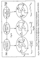
- the first configuration uses multipliers and switches and is shown in FIG. 1 .
- Switch S 1 is used to select the input to the second multiplier block such that the overall transfer characteristic can either have a power of 3 or 4.
- Switch S 2 selects the output signal either from the first or second multiplier block so as to obtain the correct transfer characteristic.
- the system comprises basic multiplier cells that are only able to produce a transfer characteristic in the form of (Input r ), where the power, r, is limited to an integer number. If a system needs a power that is a real number (i.e., 2.6), a designer will tend to implement the multiplier to provide a power of 2 or 3 as an approximation. If a power of higher order, for example 7 or 8, is to be designed, then the circuit geometry will increase in size and/or complexity. Furthermore, if the system is required to be able to select from a range of power terms, numerous switches have to be implemented to select the inputs for each multiplier, and also to select the desired signal at the output. This will further increase the size of the system.
- the second configuration consists of logarithmic-exponential transforms and an amplifier.
- This new representation shows that this system can be implemented using another approach.
- This approach mainly consists of 3 sections, and the block diagram for each section is shown in FIG. 2 a .
- a logarithmic transform has to be supplied to the input, where the result of the transform is (ln(Input)).
- r a constant value
- an exponential transform is done.
- FIG. 2 b A basic logarithmic amplifier is shown in FIG. 2 b .
- This basic logarithmic amplifier consists of an operational amplifier, an input resistor, R in , that is used to convert the voltage input, V input , to a current input, I s , and an NPN transistor that is used to convert the current input to a logarithmic voltage output, V output . From the transfer function of this logarithmic block as shown in FIG. 2 b , it can be seen that the output is dependent on the process parameter, I s .
- this logarithmic amplifier employs negative feedback, which means that the issue of control stability should be considered.
- this circuit exhibits a strong temperature dependence due to the thermal voltage, V T as well as V in /R in or Is. This dependence can be significantly reduced by using various compensation techniques. These compensation techniques may require extra components to be added, which would increase the circuit geometry.
- the disclosed embodiments of the present invention provide a circuit for generating a non-linear transfer characteristic.
- the circuit includes a plurality of current mirror sub-circuits operating in parallel within the circuit, each current mirror sub-circuit having an offset current applied to an output terminal of an output-side transistor of the current mirror sub-circuit for determining an output current of the current mirror sub-circuit, whereby the transfer characteristic is generated by setting the offset current of each current mirror sub-circuit at respective predetermined levels and summing the respective output currents of the current mirror sub-circuits.
- the embodiments of the present invention also provide a method for generating a non-linear transfer characteristic, including the steps of providing a circuit having a plurality of current mirror sub-circuits operating in parallel within the circuit, each current mirror sub-circuit having an offset current applied to an output terminal of an output-side transistor of the current mirror sub-circuit for determining an output current of the current mirror sub-circuit; and generating the transfer characteristic by setting the offset current of each current mirror sub-circuit at respective predetermined levels and summing the respective output currents of the current mirror sub-circuits.
- the offset current of each current mirror sub-circuit is adjustable to modify the transfer characteristic.
- the transistors of each current mirror sub-circuit are NPN bipolar junction transistors (BJTs).
- the transistors are PNP BJTs.
- the circuit is made up of a combination of NPN and PNP current mirror subcircuits.
- the transistors are NMOS or PMOS.
- positive slope components of the transfer characteristic are provided by NPN current mirror sub-circuits and negative slope components of the transfer characteristic are provided by PNP current mirror sub-circuits.
- positive slope components of the transfer characteristic are provided by PNP current mirror sub-circuits and negative slope components of the transfer characteristic are provided by NPN current mirror subcircuits.
- the embodiments of the present invention also include a system for generating a non-linear transfer characteristic, including a plurality of current mirror circuits in parallel, each current mirror circuit having an offset current applied to an output terminal of an output-side transistor of the current mirror circuit for controlling an output current thereof, wherein the offset current of each current mirror circuit is set to a respective predetermined level, and whereby the transfer characteristic is generated by summing the respective output currents of the current mirror circuits.
- the current mirror circuit of the present invention can be used in conjunction with a plurality of other current mirror circuits for generating a transfer characteristic, the circuit including matched input and output transistors connected in current mirror configuration, the output transistor having an offset current applied to an emitter terminal thereof for adjusting an output current of the current mirror circuit, whereby the output current can be summed with output currents of the other current mirror circuits to generate a piece-wise linear transfer characteristic.
- the system is a horizontal dynamic focus adjustment system for use in a cathode ray tube.
- range limits can be set as necessary, for example for a EW Pincushion curve with a W-shape form (East-West geometry correction), r 1 may be 1.5 and r 2 may be 2.5.
- r 1 may be 2.0 and r 2 may be 4.5.
- the invention does not employ negative feedback, and therefore the stability issue does not come into play. Fewer components are needed to realize the same transfer characteristic, and it does not depend on the process parameter, I s .
- the invention allows an end user of a CRT system to adjust the transfer characteristic, and hence the image displayed by the CRT, by adjusting an external offset current control.
- FIG. 1 is a block diagram of a prior art system for generating a non-linear transfer characteristic
- FIG. 2 a is a block diagram of a prior art logarithmic exponential configuration for generating a transfer characteristic
- FIG. 2 b is a schematic circuit diagram of the configuration shown in FIG. 2 a;
- FIG. 3 is an example transfer characteristic of a non-linear function
- FIG. 4 are four examples of non-linear transfer characteristics formed in a piece-wise linear manner
- FIG. 5 is a diagram of a current mirror circuit in accordance with an embodiment of the invention.
- FIG. 6 is a diagram of an example transfer characteristic of the current mirror circuit of FIG. 5 ;
- FIG. 7 is a block diagram of a system formed in accordance with an embodiment of the invention.
- FIG. 8 illustrates example transfer characteristics generated in accordance with an embodiment of the invention.
- a basic idea of the invention is to sum several piece-wise linear functions to obtain the desired transfer characteristics.
- Any function for example, logarithmic, quadratic, etc, can be approximated in the following form:
- u(t ⁇ t 0 ) is a unit step function of magnitude 1 when t>t 0 and zero otherwise.
- any kind of transfer characteristic can be approximated. It is desirable to control two parameters of each of these PWL functions: the time of the conduction corners, (i.e., t 0 , t 1 , t 2 , etc.) as shown in FIG. 3 , and also the slope at each corner.
- the circuit configuration of a current mirror, which forms the basic cell of the invention, is shown in FIG. 5 .
- the input stage consists of an NPN transistor, Q 1 , and an emitter resistor (R in ).
- the output stage consists of an NPN transistor, Q 2 , an emitter resistor (R out ), and a current source (I offset ) that is applied to the emitter of Q 2 .
- the ratio of both the transistors and resistors set the amplification factor or slope, and the I offset current is used to set the conduction corner.
- the output of the basic cell can be connected easily to other cells because of the open configuration of the circuit.
- NPN transistor cells as well as PNP transistor cells can be used to build a larger circuit having the desired transfer characteristic.
- transfer characteristics as shown in FIGS. 4 c and 4 d can be implemented with the PNP cell realizing the negative branch of the PWL function.
- the input of the basic cell is considered to be a current signal.
- the input current drives a current output of a positive or negative slope according to the cell characteristics and is generated by an input system such as a voltage-to-current converter or a transconductance system.
- N-type and P-type MOS transistors can be used with equal effect.
- the transfer characteristic is governed by a linear part and a non-linear part, given respectively by:
- Equation (3) models the conduction corner as the output transistor starts to conduct, at which point the output current is small relative to the input current.
- the potential at the base and emitter of Q 1 When an input current is present, the potential at the base and emitter of Q 1 will increase. A voltage comparison at the base and emitter of Q 2 determines whether Q 2 conducts. The potential at the emitter is set by I offset R out , and this setpoint can be changed easily through the offset current. Q 2 will start to conduct when I in R in is greater than I offset R out . The output current of this basic cell will be summed together with other cells to form the output current of the system. The number of branches in the PWL function, and hence the number of basic cells required, will depend on the complexity of the desired transfer characteristic.
- the transfer characteristic of a basic current mirror cell is shown in FIG. 6 .
- Bold lines indicate the theoretical PWL branch while dotted lines show the actual transfer characteristic of the basic cell.
- I offset By modulating the offset current I offset , it is possible to change the transfer characteristic, thereby providing a controllable adjustment.
- the output branch By increasing I offset , the output branch will shift to the right. Similarly by decreasing I offset , the output branch can be shifted to the left.
- the dotted line gives the actual transfer characteristic of the basic cell.
- the transfer characteristic of the basic cell is the same as the theoretical PWL branch except at the conduction corner. The non-linearity of the transistor effectively allows the curve to be smoothed at the conduction corner.
- W-, S-, and C-corrections can be implemented in the horizontal or vertical directions (as appropriate) for controlling the display on a CRT screen.
- FIG. 7 A block diagram of a system of an embodiment of the invention is shown in FIG. 7 .
- the input as a voltage source, V in , and hence a transconductance circuit is needed to convert the voltage input to a current input, I in .
- I in then acts as the input to a circuit comprising basic PNP or NPN cells, or both, depending on the transfer desired characteristic.
- the output is then fed into an amplitude control circuit to obtain the same magnitude at the maximum input signal for each different transfer characteristic.
- the necessity of the amplitude control circuit can be seen from FIG. 6 .
- I offset the output current amplitude is altered.
- three adjustment signals are used, namely I offset1 , I offset2 and I offset3 .
- I offset1 By modulating I offset1 the power (V in r , r is the power) of the proposed invention can be changed from r 1 to r 2 where r 1 and r 2 can be any arbitrary positive real numbers.
- I offset1 a particularly interesting aspect is that I offset2 , I offset3 can be a combination of the first I offset1 . In this way, it is possible to generate a complete transfer characteristic that is easily adjustable by way of a single or multiple current controls.
Landscapes
- Physics & Mathematics (AREA)
- Mathematical Physics (AREA)
- Engineering & Computer Science (AREA)
- Theoretical Computer Science (AREA)
- Software Systems (AREA)
- Computer Hardware Design (AREA)
- General Physics & Mathematics (AREA)
- Amplifiers (AREA)
Abstract
Description
f(Input)=Inputr(=e r(ln(Input)) In: natural log
f(t)=1(t−1)u(t−1)−(t−2)u(t−2)+2(t−3)u(t−3)−2(t−4)u(t−4)
I in R in−(I out +I offset)R out =V T ln[(I out /I in)(A E1 /A E2)] (1)
where: VT is the thermal voltage of the transistors; Iin, Iout are the current mirror input and output currents, respectively; AE1, AE2 are the emitter areas of Q1 and Q2, respectively. If MOS type devices are used instead of BJTs, the above equation will follow the model of the relevant MOS device used.
- Assumption 1: Taking the emitter area of both the input and output transistors to be the same. Hence AE1 will be equal to AE2.
- Assumption 2: At the point where the output transistor starts to conduct, Iout is small compared to Ioffset.
- Assumption 3: If RoutIoffset>RinIin, the output transistor cannot conduct, hence Iin<RoutIoffset/Rin.
Claims (31)
Applications Claiming Priority (1)
| Application Number | Priority Date | Filing Date | Title |
|---|---|---|---|
| PCT/SG2001/000025 WO2002067183A1 (en) | 2001-02-20 | 2001-02-20 | Circuit, method and system for generating a non-linear transfer characteristic |
Publications (2)
| Publication Number | Publication Date |
|---|---|
| US20040178840A1 US20040178840A1 (en) | 2004-09-16 |
| US7161411B2 true US7161411B2 (en) | 2007-01-09 |
Family
ID=20428907
Family Applications (1)
| Application Number | Title | Priority Date | Filing Date |
|---|---|---|---|
| US10/467,754 Expired - Fee Related US7161411B2 (en) | 2001-02-20 | 2001-02-20 | Circuit, method and system for generating a non-linear transfer characteristic |
Country Status (4)
| Country | Link |
|---|---|
| US (1) | US7161411B2 (en) |
| EP (1) | EP1364335B1 (en) |
| DE (1) | DE60116741D1 (en) |
| WO (1) | WO2002067183A1 (en) |
Cited By (2)
| Publication number | Priority date | Publication date | Assignee | Title |
|---|---|---|---|---|
| US20060244399A1 (en) * | 2002-09-30 | 2006-11-02 | Cirot Eric Y S | Horizontal and vertical dynamic correction in crt monitors |
| WO2020058883A1 (en) * | 2018-09-19 | 2020-03-26 | Sendyne Corporation | Improved analog computing implementing amplitude rescaling for solving non-linear differential equations and methods of use |
Families Citing this family (1)
| Publication number | Priority date | Publication date | Assignee | Title |
|---|---|---|---|---|
| US11385267B2 (en) * | 2019-02-14 | 2022-07-12 | Psemi Corporation | Power detector with wide dynamic range |
Citations (4)
| Publication number | Priority date | Publication date | Assignee | Title |
|---|---|---|---|---|
| US4525682A (en) | 1984-02-07 | 1985-06-25 | Zenith Electronics Corporation | Biased current mirror having minimum switching delay |
| US4814724A (en) * | 1986-07-15 | 1989-03-21 | Toko Kabushiki Kaisha | Gain control circuit of current mirror circuit type |
| EP0481277A2 (en) | 1990-10-15 | 1992-04-22 | National Semiconductor Corporation | Current source |
| US5627486A (en) * | 1994-11-29 | 1997-05-06 | Linear Technology Corporation | Current mirror circuits and methods with guaranteed off state and amplifier circuits using same |
-
2001
- 2001-02-20 DE DE60116741T patent/DE60116741D1/en not_active Expired - Fee Related
- 2001-02-20 US US10/467,754 patent/US7161411B2/en not_active Expired - Fee Related
- 2001-02-20 WO PCT/SG2001/000025 patent/WO2002067183A1/en active IP Right Grant
- 2001-02-20 EP EP01914316A patent/EP1364335B1/en not_active Expired - Lifetime
Patent Citations (4)
| Publication number | Priority date | Publication date | Assignee | Title |
|---|---|---|---|---|
| US4525682A (en) | 1984-02-07 | 1985-06-25 | Zenith Electronics Corporation | Biased current mirror having minimum switching delay |
| US4814724A (en) * | 1986-07-15 | 1989-03-21 | Toko Kabushiki Kaisha | Gain control circuit of current mirror circuit type |
| EP0481277A2 (en) | 1990-10-15 | 1992-04-22 | National Semiconductor Corporation | Current source |
| US5627486A (en) * | 1994-11-29 | 1997-05-06 | Linear Technology Corporation | Current mirror circuits and methods with guaranteed off state and amplifier circuits using same |
Non-Patent Citations (1)
| Title |
|---|
| Miropol'skiy, Y., "A Squarer," Telecommunications and Radio Engineering 46(6):70-72, Jun. 1991. |
Cited By (3)
| Publication number | Priority date | Publication date | Assignee | Title |
|---|---|---|---|---|
| US20060244399A1 (en) * | 2002-09-30 | 2006-11-02 | Cirot Eric Y S | Horizontal and vertical dynamic correction in crt monitors |
| US7777432B2 (en) * | 2002-09-30 | 2010-08-17 | Stmicroelectronics Asia Pacific Pte. Ltd. | Horizontal and vertical dynamic correction in CRT monitors |
| WO2020058883A1 (en) * | 2018-09-19 | 2020-03-26 | Sendyne Corporation | Improved analog computing implementing amplitude rescaling for solving non-linear differential equations and methods of use |
Also Published As
| Publication number | Publication date |
|---|---|
| EP1364335B1 (en) | 2006-01-18 |
| EP1364335A1 (en) | 2003-11-26 |
| US20040178840A1 (en) | 2004-09-16 |
| DE60116741D1 (en) | 2006-04-06 |
| WO2002067183A1 (en) | 2002-08-29 |
Similar Documents
| Publication | Publication Date | Title |
|---|---|---|
| US7813150B2 (en) | Compensation for parameter variations in a feedback circuit | |
| US6373330B1 (en) | Bandgap circuit | |
| JP2971552B2 (en) | Display device | |
| US5389893A (en) | Circuit for a controllable amplifier | |
| US7161411B2 (en) | Circuit, method and system for generating a non-linear transfer characteristic | |
| JPH0478208B2 (en) | ||
| US7145389B2 (en) | Temperature controlled, log-linear gain control circuit for amplifiers | |
| US4633144A (en) | Dynamic focus signal shaper | |
| US6466085B2 (en) | Amplifier circuit and preconditioning circuit for use in amplifier circuit | |
| US5814952A (en) | Device for correcting the ramp linearity of saw-tooth signals | |
| US5886677A (en) | Frame size regulating circuit | |
| KR101258281B1 (en) | Voltage to current converter and method for converting | |
| US6614284B1 (en) | PNP multiplier | |
| US5748041A (en) | AGC amplifier circuit using triple-tail cell | |
| US5942861A (en) | Front/back porch voltage-regulator of vertical focus control signal | |
| JPH0722247B2 (en) | Feedback amplifier | |
| US5153528A (en) | Gain control type amplifying apparatus | |
| JP2784803B2 (en) | Line signal generator | |
| KR930010029B1 (en) | Timebase circuit | |
| JPH07107323A (en) | Video display device | |
| JP2624338B2 (en) | Automatic duty adjustment circuit | |
| US11664799B2 (en) | Analog switch circuit and control circuit and control method thereof | |
| JP2752020B2 (en) | Gamma correction circuit for liquid crystal display | |
| JPH07202593A (en) | Voltage current conversion circuit | |
| JPS6327461Y2 (en) |
Legal Events
| Date | Code | Title | Description |
|---|---|---|---|
| AS | Assignment |
Owner name: STMICROELECTRONICS ASIA PACIFIC PTE LTD., SINGAPOR Free format text: ASSIGNMENT OF ASSIGNORS INTEREST;ASSIGNORS:CIROT, ERIC YVES SERGE;TAN, SZE KWANG;PADALA, MALLIKARJUNA RAO;REEL/FRAME:015445/0157;SIGNING DATES FROM 20040218 TO 20040229 |
|
| FEPP | Fee payment procedure |
Free format text: PAYOR NUMBER ASSIGNED (ORIGINAL EVENT CODE: ASPN); ENTITY STATUS OF PATENT OWNER: LARGE ENTITY |
|
| FEPP | Fee payment procedure |
Free format text: PAYER NUMBER DE-ASSIGNED (ORIGINAL EVENT CODE: RMPN); ENTITY STATUS OF PATENT OWNER: LARGE ENTITY Free format text: PAYOR NUMBER ASSIGNED (ORIGINAL EVENT CODE: ASPN); ENTITY STATUS OF PATENT OWNER: LARGE ENTITY |
|
| FPAY | Fee payment |
Year of fee payment: 4 |
|
| FPAY | Fee payment |
Year of fee payment: 8 |
|
| FEPP | Fee payment procedure |
Free format text: MAINTENANCE FEE REMINDER MAILED (ORIGINAL EVENT CODE: REM.); ENTITY STATUS OF PATENT OWNER: LARGE ENTITY |
|
| LAPS | Lapse for failure to pay maintenance fees |
Free format text: PATENT EXPIRED FOR FAILURE TO PAY MAINTENANCE FEES (ORIGINAL EVENT CODE: EXP.); ENTITY STATUS OF PATENT OWNER: LARGE ENTITY |
|
| STCH | Information on status: patent discontinuation |
Free format text: PATENT EXPIRED DUE TO NONPAYMENT OF MAINTENANCE FEES UNDER 37 CFR 1.362 |
|
| FP | Lapsed due to failure to pay maintenance fee |
Effective date: 20190109 |