EP0651532A2 - Procédé pour le chiffrage/déchiffrage séquentiel du code source d'un ordinateur, enregistré de façon externe - Google Patents
Procédé pour le chiffrage/déchiffrage séquentiel du code source d'un ordinateur, enregistré de façon externe Download PDFInfo
- Publication number
- EP0651532A2 EP0651532A2 EP94117097A EP94117097A EP0651532A2 EP 0651532 A2 EP0651532 A2 EP 0651532A2 EP 94117097 A EP94117097 A EP 94117097A EP 94117097 A EP94117097 A EP 94117097A EP 0651532 A2 EP0651532 A2 EP 0651532A2
- Authority
- EP
- European Patent Office
- Prior art keywords
- instruction
- instructions
- value
- enciphered
- stored
- Prior art date
- Legal status (The legal status is an assumption and is not a legal conclusion. Google has not performed a legal analysis and makes no representation as to the accuracy of the status listed.)
- Withdrawn
Links
- 238000000034 method Methods 0.000 title claims description 29
- 230000001131 transforming effect Effects 0.000 claims abstract description 8
- 238000010586 diagram Methods 0.000 description 15
- 230000008569 process Effects 0.000 description 6
- 230000004044 response Effects 0.000 description 6
- 230000006870 function Effects 0.000 description 3
- 230000008901 benefit Effects 0.000 description 2
- 230000005540 biological transmission Effects 0.000 description 2
- 230000008859 change Effects 0.000 description 1
- 238000004590 computer program Methods 0.000 description 1
- 230000000737 periodic effect Effects 0.000 description 1
- 238000009877 rendering Methods 0.000 description 1
- 230000001360 synchronised effect Effects 0.000 description 1
- 230000009466 transformation Effects 0.000 description 1
Images


Classifications
-
- G—PHYSICS
- G06—COMPUTING; CALCULATING OR COUNTING
- G06F—ELECTRIC DIGITAL DATA PROCESSING
- G06F12/00—Accessing, addressing or allocating within memory systems or architectures
- G06F12/14—Protection against unauthorised use of memory or access to memory
-
- G—PHYSICS
- G06—COMPUTING; CALCULATING OR COUNTING
- G06F—ELECTRIC DIGITAL DATA PROCESSING
- G06F21/00—Security arrangements for protecting computers, components thereof, programs or data against unauthorised activity
- G06F21/10—Protecting distributed programs or content, e.g. vending or licensing of copyrighted material ; Digital rights management [DRM]
- G06F21/12—Protecting executable software
- G06F21/121—Restricting unauthorised execution of programs
- G06F21/123—Restricting unauthorised execution of programs by using dedicated hardware, e.g. dongles, smart cards, cryptographic processors, global positioning systems [GPS] devices
-
- G—PHYSICS
- G06—COMPUTING; CALCULATING OR COUNTING
- G06F—ELECTRIC DIGITAL DATA PROCESSING
- G06F21/00—Security arrangements for protecting computers, components thereof, programs or data against unauthorised activity
- G06F21/10—Protecting distributed programs or content, e.g. vending or licensing of copyrighted material ; Digital rights management [DRM]
- G06F21/12—Protecting executable software
- G06F21/121—Restricting unauthorised execution of programs
- G06F21/125—Restricting unauthorised execution of programs by manipulating the program code, e.g. source code, compiled code, interpreted code, machine code
-
- H—ELECTRICITY
- H04—ELECTRIC COMMUNICATION TECHNIQUE
- H04L—TRANSMISSION OF DIGITAL INFORMATION, e.g. TELEGRAPHIC COMMUNICATION
- H04L9/00—Cryptographic mechanisms or cryptographic arrangements for secret or secure communications; Network security protocols
-
- H—ELECTRICITY
- H04—ELECTRIC COMMUNICATION TECHNIQUE
- H04L—TRANSMISSION OF DIGITAL INFORMATION, e.g. TELEGRAPHIC COMMUNICATION
- H04L9/00—Cryptographic mechanisms or cryptographic arrangements for secret or secure communications; Network security protocols
- H04L9/06—Cryptographic mechanisms or cryptographic arrangements for secret or secure communications; Network security protocols the encryption apparatus using shift registers or memories for block-wise or stream coding, e.g. DES systems or RC4; Hash functions; Pseudorandom sequence generators
- H04L9/065—Encryption by serially and continuously modifying data stream elements, e.g. stream cipher systems, RC4, SEAL or A5/3
-
- G—PHYSICS
- G06—COMPUTING; CALCULATING OR COUNTING
- G06F—ELECTRIC DIGITAL DATA PROCESSING
- G06F2221/00—Indexing scheme relating to security arrangements for protecting computers, components thereof, programs or data against unauthorised activity
- G06F2221/21—Indexing scheme relating to G06F21/00 and subgroups addressing additional information or applications relating to security arrangements for protecting computers, components thereof, programs or data against unauthorised activity
- G06F2221/2107—File encryption
Definitions
- the present invention relates generally to a method for rendering it difficult to break a computer object code which has been enciphered and stored in an external memory, and more specifically to such a method for transforming the enciphered computer object code into the original one while executing the same.
- a cipher is a secret method of writing whereby plaintext (or cleartext) is transformed into the corresponding ciphertext (sometimes called a cryptogram).
- plaintext or cleartext
- ciphertext sometimes called a cryptogram
- the process is called encipherment or encryption, while the reverse process of transforming ciphertext into the corresponding plaintext is called decipherment or decryption.
- Fig. 1 is a block diagram schematically showing a data transmission system wherein data to be transmitted is subject to encipherment and the data received is transformed into the original data.
- the system shown in Fig. 1 generally includes two transceivers 10a and 10b which are interconnected via a transmission channel 12. It is to be noted that the transceivers 10a and 10b are not shown in a complete manner for the sake of simplifying the disclosure.
- the transceiver 10a includes an encipherment circuit 14a, a decipherment circuit 16a, and a duplexer 18a.
- the transceiver 10b includes an encipherment circuit 14b, a decipherment circuit 16b, and a duplexer 18b.
- the encipherment circuit 14a transforms the data to be transmitted into the corresponding ciphertext.
- the enciphered data is then forwarded to the transceiver 10b whereat the transmitted data is reverse processed for obtaining the corresponding plaintext at the decipherment circuit 16b.
- the encipherment circuit 14b enciphers the data to be transmitted.
- the enciphered data is sent to the transceiver 10a wherein the transmitted data is subject to decipherment and thus transformed into the corresponding plaintext at the decipherment circuit 16a.
- Fig. 2 is a block diagram schematically showing one example of the encipherment circuit 14a.
- the other encipherment circuit 14b is configured in exactly the same manner as the circuit 14a.
- the encipherment circuit 14a includes a memory 20 in which a lookup table is stored, a selector 22, a memory 24 in which an initial value (code) is stored, a controller 26, a latch 28, and an exclusive-OR gate 30.
- the memory 20 typically takes the form of ROM (read only memory) in which a lookup table such as depicted in Fig. 3 is stored.
- each data to be transmitted has a bit length of 4.
- Fig. 4 is an illustration showing encipherment being implemented at the encipherment circuit 14a of Fig. 2, using the lookup table of Fig. 3.
- the controller 26 issues selector and latch control signals each of which assumes a logic level “1" (for example).
- the selector 22 in response to a logic level "1" of the selector control signal, selects the initial value "1101".
- the latch 28 keeps the initial value "1101” and applies same to the exclusive-OR gate 30 in response to the latch control signal assuming a logic level "1". Therefore, the exclusive-OR gate 30 outputs a transformed data (viz., enciphered data) "0100".
- the above mentioned operations are implemented within one time slot.
- the first data is applied to the lookup table 20 from which the corresponding data "1101" is outputted as shown in Fig. 4.
- the controller 26 issues the selector control signal which in turn assumes a logic level "0".
- the selector 22 in response to the selector control signal, selects the output of the memory 20 (viz., "1101") which is latched and then applied to the exclusive-OR gate 30.
- the second original data "1110” is thus transformed into "0011” at the exclusive-OR gate 30 as shown in Fig. 4. These operations are implemented within one time slot. Encipherment of the incoming data are repeated until one data sequence is terminated.
- Fig. 5 shows the decipherment circuit 16b in schematic block diagram form. Since decipherment is a reverse process of encipherment, the arrangement of Fig. 5 is similar to that of Fig. 2. Therefore, each of the function blocks of Fig. 5, which corresponds to the counterpart of Fig. 2, is designated by the same numeral with a prime.
- Fig. 5 The operation of Fig. 5 arrangement is discussed with reference to Fig. 6.
- the data sequence enciphered at the transceiver 10a is applied to the decipherment circuit 16b. That is, the data sequence is comprised of "0100”, "0011”, “1011”, “1110”, “1000”, “1110”, “0010”, “1100”, ... as shown.
- the controller 26' issues a selector control signal and a latch control signal each of which assumes a logic level “1" (for example).
- the selector 22' in response to a logic level "1" of the selector control signal, selects the initial value which is identical to the initial value used in the encipherment (viz., "1101").
- the latch 28 latches the initial value "1101” in response to the latch control signal assuming a logic level "1".
- the initial value "1101” is applied to the exclusive-OR gate 30' which in turn outputs the corresponding original data "1001".
- the original data deciphered is applied to the memory 20' which has previously stored the same lookup table as shown in Fig. 3.
- the data "1101” is obtained from the memory 20'.
- the second deciphered data "0011” is applied to the exclusive-OR gate 30'.
- the controller 26' issues the selector control signal assuming a logic level "0".
- the selector 22' responds thereto and selects the output of the memory 20' (viz., "1101") which is latched and applied to the exclusive-OR gate 30'. Accordingly, the second enciphered data "0011” is transformed into the corresponding original data "1110" at the exclusive-OR gate 30'.
- the above mentioned operations are implemented during one time slot. Following this, the decipherment circuit 16b continues to decipher the incoming deciphered data up to the completion of the decipherment of one data sequence.
- each data of the sequence except for the initial one, is enciphered or deciphered using the immediately preceding one. Therefore, even if the initial value is known an unauthorized person(s), breaking the cipher is extremely difficult as long as the content of the lookup table is kept secret.
- Another object of the present invention is to provide a method for effectively protecting computer object code against cryptanalysis.
- the above objects are achieved by the techniques wherein in order to transform enciphered instructions stored in an external memory into the original ones while a microcomputer executes the same, the instructions have been enciphered and stored in the memory such as to be logically partitioned into a plurality of groups.
- the enciphered instructions are read out of the memory for decipherment.
- a first instruction located at an initial storage address of a group is initially deciphered using a first value. Thereafter, the following instructions in the group are sequentially deciphered using a second value which is determined by transforming an immediately preceding instruction. If the microcomputer executes a branch instruction, the execution control is transferred to a branched address.
- a first instruction located at the group, which includes the branched address is deciphered using the first value.
- the instruction(s) following the first instruction are deciphered, using the second value, until deciphering an instruction stored at the branched address.
- a first aspect of the present invention resides in a method of sequentially enciphering a plurality of instructions of a computer object code, the enciphered instructions being stored in a memory, the method comprising the steps of: enciphering, using a first value, each of first instructions if the first instruction is supplied for encipherment, the plurality of first instructions being separately located, in the computer object code, away from an adjacent first instruction by a predetermined number of instructions; and enciphering, using a second value, each of a plurality of instructions other than the first instructions, the second value being determined by transforming an immediately preceding instruction.
- a further aspect of the present invention resides in a method of deciphering a plurality of instructions stored in an external memory after being enciphered, the plurality of instructions having being logically partitioned into a plurality of groups in the external memory, deciphered instructions being applied to a microcomputer and executed therein, the method comprising the steps of: reading one by one the plurality of instructions from the external memory; deciphering, using a first value, a first instruction located at an initial storage address of a group; deciphering, using a second value, each of a plurality of instructions other than the first instruction, the second value being determined by transforming an immediately preceding instruction; branching to a storage address defined by a branch instruction when the microcomputer has executed the branch instruction; deciphering, using the first value, a first instruction located at an initial storage address of a particular group which includes the branched storage address; and deciphering, using the second value, one or more than one instructions until deciphering an instruction stored at the branched storage
- the present invention is directed to transformation of enciphered computer object code, stored in an external memory, into original code while concurrently executing the code in a microcomputer (or CPU (central processing unit)).
- a microcomputer or CPU (central processing unit)
- the external memory takes the form of a RAM (random access memory), a hard disk, a floppy disc, etc.
- reference numeral 50 depicts an external memory. It is assumed, as in the related art, that each instruction of the object code has a bit length of 4 and that each storage address has also a bit length of 4. As shown, the enciphered object code is equally divided or partitioned into four instruction sequences in this particular case.
- an initial value is periodically used when the object code is enciphered before being stored into the external memory 50.
- the initial value is used each time a predetermined number of lower bits of the storage address exhibits the same value (all zeros for example).
- the predetermined number of lower bits of the storage address is set to two (2) as highlighted by underline. Therefore, the object code is equally divided into four instruction sequences each of which includes four (i.e. 22) instructions.
- the present invention is substantially identical with the related art in terms of encipherment.
- An exclusive-OR gate depicted by XOR, is supplied with the initial value "1101” and the first instruction “1001” and outputs an enciphered instruction "0100" which is stored in the external memory 50 at the storage address "00 00 ".
- This process is identical to the encipherment of the first data discussed in connection with Fig. 4.
- the following three instructions are enciphered in exactly the same manner as discussed in the opening paragraphs with Fig. 4. That is, the instructions "1110", “0011” and 1011” are respectively transformed into the corresponding enciphered ones "0011", “1011” and “1100” using the exclusive-OR gate and the lookup table shown in Fig. 3.
- the fifth instruction "0101" is to be stored at a location defined by the storage address "01 00 " and thus, the fifth instruction is subject to encipherment using the initial value "1101” as illustrated.
- the enciphered fifth instruction (viz., "1000") is stored at the location indicated by the address "0100".
- the subsequent encipherment can readily be appreciated and accordingly, further description thereof is omitted for brevity.
- the initial value "1101” is used for instruction encipherment each time an instruction needs to be stored at the address whose lower two bits exhibits " 01 ".
- the original object code has been enciphered in a manner which periodically uses the initial value, the reverse process should be implemented in order to transform the enciphered object code into the original one.
- the original code can be precisely obtained even if a branch instruction is encountered while executing the code.
- the first four instructions (viz., "0100”, “0011”, “1011” and "1100"), which has been enciphered and stored in the external memory 50, are deciphered in the same manner as in the related art.
- the first embodiment is to make available the above mentioned advantage using the following techniques. Firstly, the first code of each blocked instructions is enciphered using the initial value along the algorithm as discussed above. Secondly, when the program jumps to a certain address, the decipherment is implemented from the first address of the divided instruction sequence which includes the address to which the program execution is transferred.
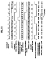
- Fig. 9 is a block diagram showing the decipherment arrangement according to the first embodiment, while Fig. 10 shows in detail an address controller 54 of Fig. 9. On the other hand, Fig. 11 is a timing chart which characterizes the operations of the arrangements of Figs. 8-10.
- the external memory 50 which has been referred to in Figs. 7 and 8, is operatively coupled to a microcomputer 52.
- the microcomputer 52 generally includes, in addition to the address controller 54, an I/O (input/output) interface 56, and a plurality of blocks 58, 20'', 22'', 24'', 28'' and 30''.
- the block 58 is comprised of CPU and an instruction decoder (neither shown).
- the block 58 will be referred to as CPU 58 for the convenience of discussion.
- the other blocks 20'', 22'', 24'', 28'' and 30'' correspond to the counterparts 20', 22', 24', 28' and 30' of Fig. 5, respectively.
- Fig. 10 is prepared to realize the principle referred to in connection with Fig. 8.
- the address controller 54 includes two selectors 60 and 62, a comparator 64, a 2-bit counter 66, and an all-zero detector 68.
- the output of the 2-bit counter 66 is synchronized or coincides with the lower 2 bits of each instruction before executing a branch instruction and after having branched to an instructed address. If the comparator 64 determines that the output of the 2-bit counter 66 does not coincide with the lower 2 bits, then the comparator 64 applies an instruction ignoring signal to the CPU 58. This signal is also applied to the selectors 60 ad 62 to change the selection of the applied signals.
- the read-out clock is used to synchronize the internal read-out signal and the memory read-out signal. While the instruction ignoring signal (or busy signal) is generated, the CPU 58 terminates the internal read-out signal as shown in Fig. 11. However, the memory read-out signal needs to be applied to the external memory 50. This is the reason why the selector 62 responds to the instruction ignoring signal and selects the read-out clock. Most of the operations have already been discussed and hence, further descriptions of Fig. 11 are deemed redundant and accordingly omitted for simplifying the instant disclosure.
- Fig. 12 is a block diagram showing a variant (depicted by 54') of the address controller 54.
- the controller 54' is configured to handle addresses having a bit length of 16.
- Each blocks of Fig. 12 are denoted by numeral attached to the counterpart of Fig. 10 plus a prime.
- the arrangement of Fig. 12 is used to transform computer object code which has been enciphered using the initial value every 16 instructions. Therefore, the lower 4 bits of the address applied to the address controller 54 is split from the total 16 bits.
- the arrangement of Fig. 12 includes 4-bit counter 66' instead of the 2-bit counter of Fig. 10. Description of Fig. 12 is omitted in that it is believed to be self-explanatory in light of the above description pertaining to the arrangement shown in Fig. 10.
- Fig. 13 is a block diagram showing a second embodiment of the present invention.
- the arrangement of Fig. 13 differs from that of Fig. 9 in that the former arrangement includes a lookup table 70 in place of the memory 24'' for storing the initial value.
- the lookup table 70 is supplied with the first address of each instruction sequence and outputs the corresponding value determined by the lookup table stored therein.
Landscapes
- Engineering & Computer Science (AREA)
- Software Systems (AREA)
- Computer Security & Cryptography (AREA)
- Theoretical Computer Science (AREA)
- Physics & Mathematics (AREA)
- General Engineering & Computer Science (AREA)
- General Physics & Mathematics (AREA)
- Computer Hardware Design (AREA)
- Technology Law (AREA)
- Multimedia (AREA)
- Radar, Positioning & Navigation (AREA)
- Remote Sensing (AREA)
- Computer Networks & Wireless Communication (AREA)
- Signal Processing (AREA)
- Storage Device Security (AREA)
Applications Claiming Priority (2)
| Application Number | Priority Date | Filing Date | Title |
|---|---|---|---|
| JP270718/93 | 1993-10-28 | ||
| JP5270718A JP2576385B2 (ja) | 1993-10-28 | 1993-10-28 | データ保護装置 |
Publications (2)
| Publication Number | Publication Date |
|---|---|
| EP0651532A2 true EP0651532A2 (fr) | 1995-05-03 |
| EP0651532A3 EP0651532A3 (fr) | 1998-01-14 |
Family
ID=17489996
Family Applications (1)
| Application Number | Title | Priority Date | Filing Date |
|---|---|---|---|
| EP94117097A Withdrawn EP0651532A3 (fr) | 1993-10-28 | 1994-10-28 | Procédé pour le chiffrage/déchiffrage séquentiel du code source d'un ordinateur, enregistré de façon externe |
Country Status (4)
| Country | Link |
|---|---|
| US (1) | US5544244A (fr) |
| EP (1) | EP0651532A3 (fr) |
| JP (1) | JP2576385B2 (fr) |
| KR (1) | KR0137709B1 (fr) |
Cited By (1)
| Publication number | Priority date | Publication date | Assignee | Title |
|---|---|---|---|---|
| GB2367657A (en) * | 2000-05-17 | 2002-04-10 | Hou Chien Tzu | Flash memory contents protection by use of a data and address scrambling IC |
Families Citing this family (11)
| Publication number | Priority date | Publication date | Assignee | Title |
|---|---|---|---|---|
| US5675645A (en) * | 1995-04-18 | 1997-10-07 | Ricoh Company, Ltd. | Method and apparatus for securing executable programs against copying |
| JPH08305558A (ja) * | 1995-04-27 | 1996-11-22 | Casio Comput Co Ltd | 暗号化プログラム演算装置 |
| US5606616A (en) * | 1995-07-03 | 1997-02-25 | General Instrument Corporation Of Delaware | Cryptographic apparatus with double feedforward hash function |
| US5710814A (en) * | 1996-07-23 | 1998-01-20 | Cheyenne Property Trust | Cryptographic unit touch point logic |
| US5724422A (en) * | 1996-08-05 | 1998-03-03 | Industrial Technology Research Institute | Encrypting and decrypting instruction boundaries of instructions in a superscalar data processing system |
| US5841870A (en) * | 1996-11-12 | 1998-11-24 | Cheyenne Property Trust | Dynamic classes of service for an international cryptography framework |
| WO1998053403A1 (fr) * | 1997-05-17 | 1998-11-26 | Young Jin Kim | Procede et appareil de protection de programme par le droit d'auteur |
| WO1999041651A2 (fr) * | 1998-02-13 | 1999-08-19 | National Computer Board, Acting Through Its R & D Division, The Information Technology Institute | Procede servant a proteger un code binaire |
| IL157854A0 (en) * | 2001-03-28 | 2004-03-28 | Digital rights management system and method | |
| JP2002328845A (ja) * | 2001-05-07 | 2002-11-15 | Fujitsu Ltd | 半導体集積回路及びicカードのセキュリティー保護方法 |
| JP5183279B2 (ja) | 2008-04-03 | 2013-04-17 | ルネサスエレクトロニクス株式会社 | 情報処理装置、命令コードの暗号化方法および暗号化命令コードの復号化方法 |
Citations (1)
| Publication number | Priority date | Publication date | Assignee | Title |
|---|---|---|---|---|
| US4562305A (en) * | 1982-12-22 | 1985-12-31 | International Business Machines Corporation | Software cryptographic apparatus and method |
Family Cites Families (3)
| Publication number | Priority date | Publication date | Assignee | Title |
|---|---|---|---|---|
| US4864494A (en) * | 1986-03-21 | 1989-09-05 | Computerized Data Ssytems For Mfg., Inc. | Software usage authorization system with key for decrypting/re-encrypting/re-transmitting moving target security codes from protected software |
| US5081675A (en) * | 1989-11-13 | 1992-01-14 | Kitti Kittirutsunetorn | System for protection of software in memory against unauthorized use |
| US5182770A (en) * | 1991-04-19 | 1993-01-26 | Geza Medveczky | System and apparatus for protecting computer software |
-
1993
- 1993-10-28 JP JP5270718A patent/JP2576385B2/ja not_active Expired - Lifetime
-
1994
- 1994-10-28 US US08/330,568 patent/US5544244A/en not_active Expired - Fee Related
- 1994-10-28 KR KR1019940027859A patent/KR0137709B1/ko not_active IP Right Cessation
- 1994-10-28 EP EP94117097A patent/EP0651532A3/fr not_active Withdrawn
Patent Citations (1)
| Publication number | Priority date | Publication date | Assignee | Title |
|---|---|---|---|---|
| US4562305A (en) * | 1982-12-22 | 1985-12-31 | International Business Machines Corporation | Software cryptographic apparatus and method |
Non-Patent Citations (1)
| Title |
|---|
| ROBERTS C E: "SYSTEM-LEVEL DATA ENCRYPTION COMES OF AGE WITH SPEED AND FLEXIBILITY" ELECTRO INTERNATIONAL CONFERENCE RECORD, vol. 17, 12 May 1992, NEW YORK, pages 336-339, XP000345009 * |
Cited By (2)
| Publication number | Priority date | Publication date | Assignee | Title |
|---|---|---|---|---|
| GB2367657A (en) * | 2000-05-17 | 2002-04-10 | Hou Chien Tzu | Flash memory contents protection by use of a data and address scrambling IC |
| GB2367657B (en) * | 2000-05-17 | 2002-08-14 | Chien-Tzu Hou | A method and apparatus for securing data contents of a non-volatile memory device |
Also Published As
| Publication number | Publication date |
|---|---|
| KR950012223A (ko) | 1995-05-16 |
| JPH07129473A (ja) | 1995-05-19 |
| EP0651532A3 (fr) | 1998-01-14 |
| JP2576385B2 (ja) | 1997-01-29 |
| US5544244A (en) | 1996-08-06 |
| KR0137709B1 (ko) | 1998-06-15 |
Similar Documents
| Publication | Publication Date | Title |
|---|---|---|
| US4386234A (en) | Cryptographic communication and file security using terminals | |
| EP0002578B1 (fr) | Méthode de communication de données | |
| EP1440535B1 (fr) | Cryptage de mémoire | |
| US4238854A (en) | Cryptographic file security for single domain networks | |
| US4227253A (en) | Cryptographic communication security for multiple domain networks | |
| EP0905942B1 (fr) | Dispositif de déchiffrage | |
| EP0840477B1 (fr) | Procédé à haute sécurité de transfert de clé secrête qui réduit les dégâts lors d'une fuite ou d'une décodage de la clé secrête | |
| US20040177257A1 (en) | Data processing device and data processing method | |
| US8577022B2 (en) | Data processing apparatus | |
| US5671284A (en) | Data encryptor having a scalable clock | |
| US5544244A (en) | Method for protecting an enciphered computer object code against cryptanalysis | |
| US20100061550A1 (en) | Data processing apparatus | |
| WO1995006373A1 (fr) | Procede et dispositif de decryptage en antememoire | |
| US8024583B2 (en) | Confidential information processing host device and confidential information processing method | |
| KR100458339B1 (ko) | 해독화방법및전자기기 | |
| EP1258796A2 (fr) | Procédé et système de protection contre la copie d'un circuit prédiffusé programmable | |
| CA2592703A1 (fr) | Systeme et procede de communication | |
| US20120321079A1 (en) | System and method for generating round keys | |
| CN109450614B (zh) | 一种适用于高速数据传输通路的加密和解密方法 | |
| CN203086489U (zh) | 一种fpga加密数据流的解密电路 | |
| CN113505399B (zh) | 一种加密芯片的烧录方法及其防篡改方法 | |
| CA2592675A1 (fr) | Systeme de communications et procede de communications associe | |
| KR100494560B1 (ko) | Rijndael암호를 이용한 블록 데이터 실시간암호복호화 장치 및 방법 | |
| WO2004105306A1 (fr) | Procede et appareil pour une implementation de la fonction d'extension de cle a faible utilisation de l'espace memoire | |
| US7613296B2 (en) | M6 block cipher system and method for encoding content and authenticating a device |
Legal Events
| Date | Code | Title | Description |
|---|---|---|---|
| PUAI | Public reference made under article 153(3) epc to a published international application that has entered the european phase |
Free format text: ORIGINAL CODE: 0009012 |
|
| AK | Designated contracting states |
Kind code of ref document: A2 Designated state(s): DE FR GB |
|
| RIN1 | Information on inventor provided before grant (corrected) |
Inventor name: OGURA, NAOYUKI |
|
| PUAL | Search report despatched |
Free format text: ORIGINAL CODE: 0009013 |
|
| RHK1 | Main classification (correction) |
Ipc: G06F 12/14 |
|
| AK | Designated contracting states |
Kind code of ref document: A3 Designated state(s): DE FR GB |
|
| 17P | Request for examination filed |
Effective date: 19971120 |
|
| STAA | Information on the status of an ep patent application or granted ep patent |
Free format text: STATUS: THE APPLICATION IS DEEMED TO BE WITHDRAWN |
|
| 18D | Application deemed to be withdrawn |
Effective date: 20020606 |