EP0651458A1 - Planar antenna and method for its manufacture - Google Patents
Planar antenna and method for its manufacture Download PDFInfo
- Publication number
- EP0651458A1 EP0651458A1 EP94402408A EP94402408A EP0651458A1 EP 0651458 A1 EP0651458 A1 EP 0651458A1 EP 94402408 A EP94402408 A EP 94402408A EP 94402408 A EP94402408 A EP 94402408A EP 0651458 A1 EP0651458 A1 EP 0651458A1
- Authority
- EP
- European Patent Office
- Prior art keywords
- layer
- support
- conductive
- organic material
- organic
- Prior art date
- Legal status (The legal status is an assumption and is not a legal conclusion. Google has not performed a legal analysis and makes no representation as to the accuracy of the status listed.)
- Granted
Links
Images

Classifications
-
- H—ELECTRICITY
- H01—ELECTRIC ELEMENTS
- H01Q—ANTENNAS, i.e. RADIO AERIALS
- H01Q9/00—Electrically-short antennas having dimensions not more than twice the operating wavelength and consisting of conductive active radiating elements
- H01Q9/04—Resonant antennas
- H01Q9/0407—Substantially flat resonant element parallel to ground plane, e.g. patch antenna
-
- H—ELECTRICITY
- H01—ELECTRIC ELEMENTS
- H01Q—ANTENNAS, i.e. RADIO AERIALS
- H01Q1/00—Details of, or arrangements associated with, antennas
- H01Q1/36—Structural form of radiating elements, e.g. cone, spiral, umbrella; Particular materials used therewith
- H01Q1/38—Structural form of radiating elements, e.g. cone, spiral, umbrella; Particular materials used therewith formed by a conductive layer on an insulating support
Definitions
- the present invention relates to a planar antenna and the method for producing such an antenna.
- the invention is situated in the context of the large telecommunications market.
- the antenna In connection equipment, the antenna is the most visible and often the most bulky outdoor sub-assembly. It must have ever better performance, for ever greater discretion, and always lower cost.
- the performance of an antenna depends on the technology chosen.
- the realization of planar antennas involves the use of supports having low losses, and a dielectric constant as low as possible.
- These supports can be made of organic materials having such characteristics. Particularly advantageous organic materials are those in expanded form or "foams".
- the constant dielectric of the latter is very close to that of air and their low losses allow a significant improvement in the performance of the antennas, particularly for frequencies around the GHz, or a few GHz. For other frequency ranges, the use of unexpanded organic supports is also possible.
- antenna designers wish to have a technology in which the conductive planes are directly associated with the foam, and deposited selectively.
- the object of the invention is to solve such a problem.
- the invention relates to a method of producing a planar antenna, operating at a frequency of a few GHz, comprising at least one circuit layer, in which, for each circuit layer, a selective metallization of a material support is carried out.
- organic having a low dielectric constant, less than 2.5, and low losses, less than 10 ⁇ 3, by depositing a layer of conductive material on all or part of at least one surface of said support, thus making it possible to define the conductive parts of this circuit, after the possible deposition of an intermediate layer intended to improve the surface condition of said support.
- metallization is carried out by direct deposition of a conductive layer on all or part of a surface of a support made of expanded organic material (organic foam), of non-organic material. expanded, or of unexpanded organic material adhering to the surface of a foam.
- expanded organic material organic foam
- non-organic material expanded, or of unexpanded organic material adhering to the surface of a foam.
- the layer of conductive material is obtained from a conductive paste with an organic binder, or from a metal or a metal alloy.
- the metallization is obtained by a screen printing, buffering, projection, spraying or plating technique. It can be followed by a transformation operation of the deposited products whose purpose is to make them adherent to the supports and good conductors. To give the metallic deposit all its conductivity, heat treatment or exposure to different radiations such as infrared or ultraviolet is carried out.
- the support can be previously shaped.
- the layer of adherent organic material can be polypropylene or a polypropylene copolymer.
- the layers are juxtaposed by pressing or calendering, while hot.
- the invention also relates to a planar antenna, operating at a frequency of a few GHz, comprising at least one circuit layer, characterized in that, for each circuit layer, it comprises a layer of conductive material on a support made of organic material, having a low dielectric constant, less than 2.5, and low losses, less than 10 ⁇ 3, on all or part of at least one surface of said support with possibly an intermediate layer intended to improve the surface condition of said support .
- the support made of organic material is made of expanded organic material (or organic foam), of unexpanded organic material, or of unexpanded organic material adhering to the surface of a foam. It may for example be a polymethacrylate imide foam.
- the layer of conductive material is made of conductive paste with an organic binder, metal, or a metal alloy. It is, for example, composed of an organic binder based on ethylcellulose charged with silver.
- the intermediate layer is for example made of polypropylene or propylene copolymer.
- the antenna of the invention may include electrical connections, between conductive planes, made using conductive paste, or by any other type of conductive material.
- At least one of its external faces can be protected by a radome which does not degrade the radio performance or little, this radome being a layer adhering to one of the external faces of the antenna.
- this radome is a layer of organic foam, or a layer of polypropylene or of polypropylene copolymer, or a protective varnish.
- the method of the invention also includes the production of antennas with multilayer circuits by association of elements defined above, as well as the production of connections between conductive layers located in different planes. It makes it possible to produce antennas by directly associating with it a protective radome or any other element, such as a polarizer, in a homogeneous form.
- the technique used to produce these antennas consists of depositing metallic materials on a support material, directly defining the geometry of the conductive parts of the circuits. This deposit is generally followed by a transformation operation of these metallic products whose purpose is to make them adherent to support materials and good conductors. It can be done by screen printing, stamping, spraying, or by any other method of deposit.
- the deposition will be carried out, by way of example, by screen printing followed by a heat treatment.
- the choice of foam as the support material 10 is first dictated by the search for advantageous electrical characteristics: a low dielectric constant, close to 1, and low losses, less than 10 ⁇ 3.
- the foam must be a rigid foam capable of withstanding temperatures at least equal to those of cooking pasta between 120 ° C and 200 ° C.
- the foam in certain cases it is advantageous, as illustrated in FIG. 3, to give the foam a particular shape, before proceeding to the selective deposition of the conducting parts 11.
- the shaping of the foam can be obtained by cold pressing or by hot thereof in a suitable mold, or by mechanical machining.
- this conductive paste can intervene in the choice of this conductive paste such as for example the fact of being able to obtain a good definition of the circuits carried out or good solderability, etc.
- the circuits are produced by screen printing.
- certain precautions must be observed: obtaining the best possible definition of the geometries and good regularity of thickness is necessary.
- the precision of alignment of the patterns from one face to the other face of the foam is important.
- the surface of a foam often has a relatively high roughness, which can affect the accuracy of the conductors.
- Such a layer 12 has the effect of improving the surface condition.
- the insulating paste must be chosen so as not to disturb, or disturb as little as possible, the electrical characteristics of the support. It may be interesting to choose the organic vehicle constituting the conductive paste. After polymerization of this insulating layer, the antenna is produced with the conventional screen printing technique.
- the choice of the support material is again a function of its dielectric characteristics: the losses must be less than 10Mites3, on the other hand the dielectric constant, generally higher than for foams, is of the order of 2. The material must be able to withstand temperatures equal to the cooking temperatures of the pasta.
- the implementation of the antenna production technology on such a material does not differ significantly from that used on a foam.
- the surface condition of the material being better than in the case of foams, the deposits of metallic products obtained are generally of better quality.
- thermoplastic material is also chosen as a function of its low dielectric constant and of its low losses. In addition, its softening temperature must be lower than the deformation temperature under load of the foam.
- connection between the various circuits is made by means of a thin thermoplastic film 13, chosen according to the criteria for choosing the support material, as defined above.
- its softening temperature must be lower than that of the support materials previously defined.
- Its implementation cycle includes a temperature-pressure juxtaposition.
- These connections can be made in different ways known to those skilled in the art, for example by metallization using conductive pastes, or by metal inserts.
- the printed antennas require protection with respect to the environment by a radome 16.
- This can be produced using a layer of organic material, expanded or not.
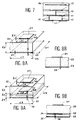
- the attachment of such a radome to the antenna which has just been described can be carried out, as illustrated in FIG. 7, using the technique for producing an antenna comprising several dielectric levels. previously described.
- the antenna is presented as a double-sided printed circuit, as illustrated in FIGS. 8A and 8B.
- the metal deposits 21 and 22 are produced by screen printing of a paste composed of an organic binder based on ethylcellulose charged with silver as described above.
- This antenna is supplied by a coaxial probe 23 located on the median of the radiating element 21 at a distance of 10.25 mm from the center.
- This antenna transmits in the L band around 2 GHz.
- the radioelectric characteristics of this one were measured and are gathered in the following table: Resonance frequency 1.975 GHz Bandwidth at ROS ⁇ 1.5 2.2% Gain 7.5 dB
- the antenna is an antenna with two coupled radiating elements, produced on a laminate associating foam and unexpanded polymer.
- the antenna is presented as a two-layer antenna produced as illustrated in FIGS. 9A and 9B.
- the antenna is supplied on the diagonal by a probe 36, at the level of the lower conductor 34, at a distance of 41 mm from the center.
- This antenna transmits in the L band around 1.5 GHz. Its characteristics have been measured and gathered in the following table: Resonance frequency 1,490 - 1,640 GHz Bandwidth at ROS ⁇ 1.5 11.5% Gain 9.52 dB Opening to 3dB plans E and H 60 °
- This type of antenna can be entirely realized with all the conductive levels obtained using screen-printed silver paste.
Landscapes
- Details Of Aerials (AREA)
- Waveguide Aerials (AREA)
Abstract
Description
La présente invention concerne une antenne plane et le procédé de réalisation d'une telle antenne.The present invention relates to a planar antenna and the method for producing such an antenna.
L'invention se situe dans le cadre du grand marché des Télécommunications. On assiste, en effet, depuis quelques années au décollement sans précédent d'un nouveau service des Télécommunications, celui des liaisons avec des terminaux mobiles appelés couramment "mobiles". Ces liaisons sont à considérer tant pour les liaisons systèmes fixes à mobiles que pour les liaisons entre mobiles.The invention is situated in the context of the large telecommunications market. In recent years, we have witnessed the unprecedented take-off of a new telecommunications service, that of links with mobile terminals commonly known as "mobile". These connections are to be considered both for fixed system to mobile links and for links between mobiles.
De telles liaisons sont rendues possibles grâce aux énormes progrès faits dans le domaine de l'électronique, en particulier celui des composants intégrés (M.M.I.C.), et celui des sources d'énergie (piles-batteries).Such connections are made possible thanks to the enormous progress made in the field of electronics, in particular that of integrated components (M.M.I.C.), and that of energy sources (batteries).
Dans un équipement de liaison, l'antenne est le sous-ensemble extérieur le plus visible et souvent le plus encombrant. Elle doit avoir des performances toujours meilleures, pour une discrétion toujours plus grande, et un coût toujours plus bas.In connection equipment, the antenna is the most visible and often the most bulky outdoor sub-assembly. It must have ever better performance, for ever greater discretion, and always lower cost.
Après un travail de recherche intensif mené chez les universitaires comme chez les industriels des pays les plus développés, il est apparu que les antennes dites "imprimées" ou "planes" représentaient la meilleure solution possible.After intensive research work carried out by academics and industrialists in the most developed countries, it appeared that so-called "printed" or "flat" antennas represented the best possible solution.
Les performances d'une antenne dépendent de la technologie choisie. La réalisation d'antennes planes implique l'utilisation de supports présentant de faibles pertes, et une constante diélectrique la plus faible possible. Ces supports peuvent être réalisés en matériaux organiques présentant de telles caractéristiques. Des matériaux organiques particulièrement avantageux sont ceux se présentant sous forme expansée ou "mousses". La constante diélectrique de ces dernières est très proche de celle de l'air et leurs faibles pertes permettent une amélioration sensible des performances des antennes, particulièrement pour des fréquences situées autour du GHz, ou de quelques GHz. Pour d'autres domaines de fréquences, l'utilisation de supports organiques non expansés est aussi possible.The performance of an antenna depends on the technology chosen. The realization of planar antennas involves the use of supports having low losses, and a dielectric constant as low as possible. These supports can be made of organic materials having such characteristics. Particularly advantageous organic materials are those in expanded form or "foams". The constant dielectric of the latter is very close to that of air and their low losses allow a significant improvement in the performance of the antennas, particularly for frequencies around the GHz, or a few GHz. For other frequency ranges, the use of unexpanded organic supports is also possible.
Jusqu'à présent les différentes mousses disponibles sont utilisées comme interface entre plusieurs plans conducteurs et maintenues mécaniquement pour servir :
- de diélectrique ;
- de radôme ;
- de rigidificateur.
- dielectric;
- radome;
- stiffener.
Mais de telles réalisations impliquent un certain nombre de contraintes, du fait des constituants qu'il faut assembler avec précision, et qui ne permettent pas nécessairement une grande facilité d'intégration.However, such embodiments imply a certain number of constraints, because of the constituents which have to be assembled with precision, and which do not necessarily allow great ease of integration.
Aussi, actuellement, les concepteurs d'antennes souhaitent disposer d'une technologie dans laquelle les plans conducteurs seraient directement associés à la mousse, et déposés sélectivement.Also, currently, antenna designers wish to have a technology in which the conductive planes are directly associated with the foam, and deposited selectively.
L'invention a pour objet de résoudre un tel problème.The object of the invention is to solve such a problem.
L'invention concerne un procédé de réalisation d'une antenne plane, fonctionnant à une fréquence de quelques GHz, comprenant au moins une couche de circuit, dans lequel, pour chaque couche de circuit, on réalise une métallisation sélective d'un support en matériau organique, présentant une faible constante diélectrique, inférieure à 2,5 , et de faibles pertes, inférieures à 10⁻³, par dépôt d'une couche de matériau conducteur sur tout ou partie d'au moins une surface dudit support, permettant ainsi de définir les parties conductrices de ce circuit, après le dépôt éventuel d'une couche intermédiaire destinée à améliorer l'état de surface dudit support.The invention relates to a method of producing a planar antenna, operating at a frequency of a few GHz, comprising at least one circuit layer, in which, for each circuit layer, a selective metallization of a material support is carried out. organic, having a low dielectric constant, less than 2.5, and low losses, less than 10⁻³, by depositing a layer of conductive material on all or part of at least one surface of said support, thus making it possible to define the conductive parts of this circuit, after the possible deposition of an intermediate layer intended to improve the surface condition of said support.
Avantageusement, on réalise une métallisation par dépôt direct d'une couche conductrice sur tout ou partie d'une surface d'un support en matériau organique expansé (mousse organique), en matériau organique non expansé, ou en matériau organique non expansé adhérant à la surface d'une mousse.Advantageously, metallization is carried out by direct deposition of a conductive layer on all or part of a surface of a support made of expanded organic material (organic foam), of non-organic material. expanded, or of unexpanded organic material adhering to the surface of a foam.
La couche de matériau conducteur est obtenue à partir d'une pâte conductrice à liant organique, ou à partir d'un métal ou un alliage de métaux. La métallisation est obtenue par une technique de sérigraphie, de tamponnage, de projection, de pulvérisation ou de placage. Elle peut être suivie d'une opération de transformation des produits déposés ayant pour objet de les rendre adhérents aux supports et bons conducteurs. Pour donner au dépôt métallique toute sa conductivité, on réalise un traitement thermique ou une exposition à différents rayonnements tels que infrarouge, ou ultraviolet.The layer of conductive material is obtained from a conductive paste with an organic binder, or from a metal or a metal alloy. The metallization is obtained by a screen printing, buffering, projection, spraying or plating technique. It can be followed by a transformation operation of the deposited products whose purpose is to make them adherent to the supports and good conductors. To give the metallic deposit all its conductivity, heat treatment or exposure to different radiations such as infrared or ultraviolet is carried out.
Dans certains exemples de réalisation, le support peut être préalablement mis en forme.In some exemplary embodiments, the support can be previously shaped.
On peut reporter sur au moins une des faces de l'antenne, une (ou plusieurs) couche(s) de matériaux supports métallisés en intercalant une (ou plusieurs) feuille(s) de matériau organique adhérent. La couche de matériau organique adhérent peut être du polypropylène ou un copolymère de polypropylène. La juxtaposition des couches est réalisée par pressage ou calandrage, à chaud.It is possible to transfer onto at least one of the faces of the antenna, one (or more) layer (s) of metallized support materials by interposing one (or more) sheet (s) of adherent organic material. The layer of adherent organic material can be polypropylene or a polypropylene copolymer. The layers are juxtaposed by pressing or calendering, while hot.
L'invention concerne également une antenne plane, fonctionnant à une fréquence de quelques GHz, comprenant au moins une couche de circuit, caractérisée en ce que, pour chaque couche de circuit, elle comprend une couche de matériau conducteur sur un support en matériau organique, présentant une faible constante diélectrique, inférieure à 2,5 , et de faibles pertes, inférieures à 10⁻³, sur tout ou partie d'au moins une surface dudit support avec éventuellement une couche intermédiaire destinée à améliorer l'état de surface dudit support.The invention also relates to a planar antenna, operating at a frequency of a few GHz, comprising at least one circuit layer, characterized in that, for each circuit layer, it comprises a layer of conductive material on a support made of organic material, having a low dielectric constant, less than 2.5, and low losses, less than 10⁻³, on all or part of at least one surface of said support with possibly an intermediate layer intended to improve the surface condition of said support .
Avantageusement, le support en matériau organique est réalisé en matériau organique expansé (ou mousse organique), en matériau organique non expansé, ou en matériau organique non expansé adhérant à la surface d'une mousse. Ce peut être par exemple une mousse d'imide de polyméthacrylate. La couche de matériau conducteur est en pâte conductrice à liant organique, en métal, ou en alliage de métal. Elle est, par exemple, composée d'un liant organique à base d'éthylcellulose chargée à l'argent. La couche intermédiaire est par exemple réalisée en polypropylène ou en copolymère de propylène.Advantageously, the support made of organic material is made of expanded organic material (or organic foam), of unexpanded organic material, or of unexpanded organic material adhering to the surface of a foam. It may for example be a polymethacrylate imide foam. The layer of conductive material is made of conductive paste with an organic binder, metal, or a metal alloy. It is, for example, composed of an organic binder based on ethylcellulose charged with silver. The intermediate layer is for example made of polypropylene or propylene copolymer.
L'antenne de l'invention peut comporter des liaisons électriques, entre plans conducteurs, réalisées à l'aide de pâte conductrice, ou par tout autre type de matériau conducteur.The antenna of the invention may include electrical connections, between conductive planes, made using conductive paste, or by any other type of conductive material.
Au moins une de ses faces extérieures peut être protégée par un radôme ne dégradant pas ou peu les performances radioélectriques, ce radôme étant une couche adhérant à l'une des faces extérieures de l'antenne. Avantageusement, ce radôme est une couche de mousse organique, ou une couche de polypropylène ou en copolymère de polypropylène, ou un vernis protecteur.At least one of its external faces can be protected by a radome which does not degrade the radio performance or little, this radome being a layer adhering to one of the external faces of the antenna. Advantageously, this radome is a layer of organic foam, or a layer of polypropylene or of polypropylene copolymer, or a protective varnish.
- Les figures 1 à 7 illustrent différentes caractéristiques de l'invention ;Figures 1 to 7 illustrate different features of the invention;
- les figures 8A et 8B illustrent une première réalisation avantageuse de l'invention ;FIGS. 8A and 8B illustrate a first advantageous embodiment of the invention;
- la figure 9A et 9B illustre une seconde réalisation avantageuse de l'invention.FIG. 9A and 9B illustrates a second advantageous embodiment of the invention.
Le procédé de l'invention concerne la réalisation d'antennes imprimées par dépôt sélectif d'une couche conductrice soit :
- sur une mousse organique ;
- sur un polymère non expansé ;
- sur un stratifié associant mousse et polymère non expansé.
- on an organic foam;
- on an unexpanded polymer;
- on a laminate combining foam and unexpanded polymer.
Le procédé de l'invention inclut aussi la réalisation d'antennes à circuits multicouches par association d'éléments ci-dessus définis, de même que la réalisation de liaisons entre couches conductrices situées dans des plans différents. Il permet de réaliser des antennes en y associant directement un radôme de protection ou tout autre élément, comme un polariseur, sous une forme homogène.The method of the invention also includes the production of antennas with multilayer circuits by association of elements defined above, as well as the production of connections between conductive layers located in different planes. It makes it possible to produce antennas by directly associating with it a protective radome or any other element, such as a polarizer, in a homogeneous form.
Selon l'invention, la technique utilisée pour réaliser ces antennes consiste en un dépôt sur un matériau support de produits métalliques, définissant directement la géométrie des parties conductrices des circuits. Ce dépôt est suivi généralement d'une opération de transformation de ces produits métalliques ayant pour objet de les rendre adhérents aux matériaux supports et bons conducteurs. Il peut se faire par sérigraphie, tamponnage, pistolettage, ou par tout autre mode de dépôt. Un traitement ayant pour objet de donner au dépôt toute sa conductibilité, par exemple un traitement thermique, un exposition à différents rayonnements : infrarouge, ultraviolet..., peut également être réalisé.According to the invention, the technique used to produce these antennas consists of depositing metallic materials on a support material, directly defining the geometry of the conductive parts of the circuits. This deposit is generally followed by a transformation operation of these metallic products whose purpose is to make them adherent to support materials and good conductors. It can be done by screen printing, stamping, spraying, or by any other method of deposit. A treatment having for object to give to the deposit all its conductivity, for example a heat treatment, an exposure to different radiations: infrared, ultraviolet ..., can also be carried out.
Dans la description qui suit, le dépôt sera réalisé, à titre d'exemple, par sérigraphie suivi d'un traitement thermique.In the description which follows, the deposition will be carried out, by way of example, by screen printing followed by a heat treatment.
Dans une telle réalisation, illustrée à la figure 1, pour une utilisation dans le domaine radiofréquence, le choix de la mousse comme matériau support 10 est d'abord dicté par la recherche de caractéristiques électriques intéressantes : une faible constante diélectrique, voisine de 1, et de faibles pertes, inférieures à 10⁻³. La mousse doit être une mousse rigide pouvant supporter des températures au moins égales à celles de cuisson des pâtes comprises entre 120°C et 200°C.In such an embodiment, illustrated in FIG. 1, for use in the radiofrequency field, the choice of foam as the
Dans certains cas il est intéressant, comme illustré à la figure 3, de donner à la mousse une forme particulière, avant de procéder au dépôt sélectif des parties conductrices 11. La mise en forme de la mousse peut être obtenue par pressage à froid ou à chaud de celle-ci dans un moule approprié, ou par usinage mécanique.In certain cases it is advantageous, as illustrated in FIG. 3, to give the foam a particular shape, before proceeding to the selective deposition of the conducting
La pâte conductrice 11 à sérigraphier est constituée d'éléments métalliques en suspension dans un véhicule organique. Son choix est fait selon deux critères essentiels :
- il faut qu'en final le dépôt obtenu possède la meilleure conductibilité possible ;
- il faut que ses différents constituants soient compatibles avec la nature de la mousse.
- in the end, the deposit obtained must have the best possible conductivity;
- its various constituents must be compatible with the nature of the foam.
D'autres facteurs peuvent intervenir dans le choix de cette pâte conductrice comme par exemple le fait de pouvoir obtenir une bonne définition des circuits réalisés ou une bonne soudabilité, etc....Other factors can intervene in the choice of this conductive paste such as for example the fact of being able to obtain a good definition of the circuits carried out or good solderability, etc.
Dans un exemple de réalisation, les circuits sont réalisés par sérigraphie. Toutefois, s'agissant de circuits destinés à des fréquences élevées, certaines précautions doivent être respectées : obtenir la meilleure définition possible des géométries et une bonne régularité d'épaisseur est nécessaire. Dans le cas de circuits double face, la précision d'alignement des motifs d'une face à l'autre face de la mousse est importante....In an exemplary embodiment, the circuits are produced by screen printing. However, in the case of circuits intended for high frequencies, certain precautions must be observed: obtaining the best possible definition of the geometries and good regularity of thickness is necessary. In the case of double-sided circuits, the precision of alignment of the patterns from one face to the other face of the foam is important.
De par sa nature même, la surface d'une mousse présente souvent une rugosité relativement importante, ce qui peut nuire à la précision des conducteurs. Dans certains cas, il est intéressant, comme illustré à la figure 2, de procéder au dépôt d'une pâte isolante formant une couche uniforme 12 sur une ou deux faces du matériau support 10 en mousse avant le dépôt des produits métalliques 11. Une telle couche 12 a pour effet d'améliorer l'état de surface. La pâte isolante doit être choisie de façon à ne pas perturber, ou perturber le moins possible, les caractéristiques électriques du support. Il peut être intéressant de choisir le véhicule organique constituant la pâte conductrice. Après polymérisation de cette couche isolante, la réalisation de l'antenne s'effectue avec la technique classique de sérigraphie.By its very nature, the surface of a foam often has a relatively high roughness, which can affect the accuracy of the conductors. In certain cases, it is advantageous, as illustrated in FIG. 2, to carry out the deposition of an insulating paste forming a
Dans une telle réalisation, le choix du matériau support est, là encore, fonction de ses caractéristiques diélectriques : les pertes doivent être inférieures à 10⁻³, par contre la constante diélectrique, généralement plus élevée que pour les mousses, est de l'ordre de 2. Le matériau doit pouvoir supporter des températures égales aux températures de cuisson des pâtes.In such an embodiment, the choice of the support material is again a function of its dielectric characteristics: the losses must be less than 10 inférieures³, on the other hand the dielectric constant, generally higher than for foams, is of the order of 2. The material must be able to withstand temperatures equal to the cooking temperatures of the pasta.
Le choix de la pâte conductrice se fait selon les deux critères définis ci-dessus pour la réalisation d'antennes sur mousse organique.The choice of conductive paste is made according to the two criteria defined above for the production of antennas on organic foam.
La mise en oeuvre de la technologie de réalisation d'antennes sur un tel matériau ne diffère pas sensiblement de celle utilisée sur une mousse. L'état de surface du matériau étant meilleur que dans le cas des mousses, les dépôts de produits métalliques obtenus sont généralement de meilleure qualité.The implementation of the antenna production technology on such a material does not differ significantly from that used on a foam. The surface condition of the material being better than in the case of foams, the deposits of metallic products obtained are generally of better quality.
Si compte tenu des performances requises par l'antenne l'état de surface de la mousse est pénalisante, et si les constantes diélectriques des matériaux non expansés sont trop élevées, un compromis peut être trouvé en effectuant un dépôt métallique 11 sur un stratifié constitué d'une mousse 10 recouverte sur une ou deux faces d'un polymère thermoplastique non expansé 17, comme représenté sur la figure 4. Ce stratifié peut être réalisé par exemple par une opération de pressage à chaud.If, given the performance required by the antenna, the surface condition of the foam is penalizing, and if the dielectric constants of the unexpanded materials are too high, a compromise can be found by carrying out a
Le choix de la mousse se fait en fonction des critères définis précédemment. S'y ajoute une obligation, celle de pouvoir supporter des pressions de quelques bars à une température égale ou supérieure à 120°C.The choice of foam is made according to the criteria defined above. There is also an obligation, that of being able to withstand pressures of a few bars at a temperature equal to or greater than 120 ° C.
Le matériau thermoplastique est encore choisi en fonction de sa faible constante diélectrique et de ses faibles pertes. De plus sa température de ramollissement doit être inférieure à la température de déformation sous charge de la mousse.The thermoplastic material is also chosen as a function of its low dielectric constant and of its low losses. In addition, its softening temperature must be lower than the deformation temperature under load of the foam.
Le choix de la pâte conductrice se fait selon les deux critères définis plus haut.The choice of conductive paste is made according to the two criteria defined above.
A partir de circuits réalisés selon les variantes du procédé de l'invention définies ci-dessus, il est possible, comme illustré à la figure 5, de réaliser des circuits multicouches en particulier par pressage à chaud.From circuits produced according to the variants of the method of the invention defined above, it is possible, as illustrated in FIG. 5, to produce multilayer circuits in particular by hot pressing.
La liaison entre les différents circuits se fait par l'intermédiaire d'un film thermoplastique de fine épaisseur 13, choisi selon les critères de choix du matériau support, tels que définis ci-dessus. De plus, sa température de ramollissement doit être inférieure à celle des matériaux support précédemment définis. Son cycle de mise en oeuvre comprend une juxtaposition température-pression.The connection between the various circuits is made by means of a
Comme illustré à la figure 6, il est possible de réaliser des liaisons conductrices 15 entre les différents niveaux conducteurs 11. Ces liaisons peuvent être réalisées de différentes façons connues de l'homme de l'art, par exemple par métallisation à l'aide de pâtes conductrices, ou par inserts métalliques.As illustrated in FIG. 6, it is possible to produce
Dans bon nombre de cas, les antennes imprimées nécessitent une protection vis-à-vis de l'environnement par un radôme 16. Celui-ci peut être réalisé à l'aide d'une couche de matériau organique expansé ou non. La fixation d'un tel radôme sur l'antenne qui vient d'être décrite peut être réalisée, comme illustré à la figure 7, en utilisant la technique de réalisation d'antenne comportant plusieurs niveaux diélectriques. décrite précédemment.In a good number of cases, the printed antennas require protection with respect to the environment by a
Dans un premier mode de réalisation avantageux l'antenne se présente comme un circuit imprimé double face, comme illustré sur les figures 8A et 8B.In a first advantageous embodiment, the antenna is presented as a double-sided printed circuit, as illustrated in FIGS. 8A and 8B.
Le matériau support 20 est en mousse d'imide de polyméthacrylate, de masse volumique 51 Kg/m³, possédant les caractéristiques suivantes fournies par le fabricant.
Les dépôts métalliques 21 et 22 sont réalisés par sérigraphie d'une pâte composée d'un liant organique à base d'éthylcellulose chargée à l'argent comme décrit précédemment. On a les caractéristiques suivantes :
Cette antenne est alimentée par une sonde coaxiale 23 localisée sur la médiane de l'élément rayonnant 21 à une distance de 10,25 mm du centre.This antenna is supplied by a
Cette antenne émet dans la bande L autour de 2 GHz. Les caractéristiques radioélectriques de celle-ci ont été mesurées et sont rassemblées dans le tableau suivant :
Ces résultats, ainsi que les diagrammes de rayonnement, sont tout à fait comparables à ceux obtenus avec des prototypes de laboratoire réalisés à l'aide de film de cuivre collé.These results, as well as the radiation patterns, are quite comparable to those obtained with laboratory prototypes produced using glued copper film.
Dans un second mode de réalisation avantageux, l'antenne est une antenne à deux éléments rayonnants couplés, réalisée sur un stratifié associant mousse et polymère non expansé. L'antenne se présente comme une antenne bicouche réalisée comme illustré sur les figures 9A et 9B.In a second advantageous embodiment, the antenna is an antenna with two coupled radiating elements, produced on a laminate associating foam and unexpanded polymer. The antenna is presented as a two-layer antenna produced as illustrated in FIGS. 9A and 9B.
Le dépôt métallique 31 constituant l'élément rayonnant supérieur est réalisée par sérigraphie d'une pâte composée d'un liant organique à base d'éthylcellulose chargé à l'argent comme décrit précédemment :
Epaisseur h4 = 40 µm environ
Conductivité = 50 mΩ/□
L4 = W4 = 74 mmThe
Thickness h4 = around 40 µm
Conductivity = 50 mΩ / □
L4 = W4 = 74 mm
Le matériau support 30 est une mousse d'imide de polyméthacrylate de masse volumique 51 Kg/m³ possédant les caractéristiques suivantes :
εr5 = 1.07
tgδ5 = 8.10⁻⁴
h5 = 10 mmThe
εr5 = 1.07
tgδ5 = 8.10⁻⁴
h5 = 10 mm
La couche 32 est une couche de polymère non expansé très mince d'épaisseur h6 = 20 µm et de dimensions 200 x 200 mm.
La couche 33 est une couche de polypropylène dont les caractéristiques sont les suivantes :
εr7 = 2,2
Tfδ7 = 10⁻⁴
h7= 1,6 mm
L7 = W7 = 200 mm
εr7 = 2.2
Tfδ7 = 10⁻⁴
h7 = 1.6 mm
L7 = W7 = 200 mm
Les dépôts métalliques 34 et 35 constituant respectivement le deuxième élément rayonnant et le plan de masse sont réalisés à l'aide d'un feuillard de cuivre d'épaisseur 20 µm. Leurs dimensions respectives sont les suivantes :
L8 = W8 = 64 mm
L9 = W9 = 200 mmThe
L8 = W8 = 64 mm
L9 = W9 = 200 mm
L'antenne est alimentée sur la diagonale par une sonde 36, au niveau du conducteur inférieur 34, à une distance de 41 mm du centre.The antenna is supplied on the diagonal by a
Cette antenne émet dans la bande L autour de 1,5 GHz. Ses caractéristiques ont été mesurées et rassemblées dans le tableau suivant :
Ce type d'antenne peut être entièrement réalisé avec tous les niveaux conducteurs obtenus à l'aide de pâte à l'argent sérigraphiée.This type of antenna can be entirely realized with all the conductive levels obtained using screen-printed silver paste.
Claims (28)
Applications Claiming Priority (2)
| Application Number | Priority Date | Filing Date | Title |
|---|---|---|---|
| FR9312872A FR2711845B1 (en) | 1993-10-28 | 1993-10-28 | Planar antenna and method for producing such an antenna. |
| FR9312872 | 1993-10-28 |
Publications (2)
| Publication Number | Publication Date |
|---|---|
| EP0651458A1 true EP0651458A1 (en) | 1995-05-03 |
| EP0651458B1 EP0651458B1 (en) | 2003-01-02 |
Family
ID=9452308
Family Applications (1)
| Application Number | Title | Priority Date | Filing Date |
|---|---|---|---|
| EP94402408A Expired - Lifetime EP0651458B1 (en) | 1993-10-28 | 1994-10-26 | Method for manufacturing a planar antenna |
Country Status (4)
| Country | Link |
|---|---|
| EP (1) | EP0651458B1 (en) |
| JP (1) | JPH07183722A (en) |
| DE (1) | DE69431942T2 (en) |
| FR (1) | FR2711845B1 (en) |
Cited By (6)
| Publication number | Priority date | Publication date | Assignee | Title |
|---|---|---|---|---|
| GB2312098A (en) * | 1996-04-11 | 1997-10-15 | Siemens Ag | Antenna comprising two sides of circuit board |
| WO1998013896A1 (en) * | 1996-09-23 | 1998-04-02 | Lutz Rothe | Mobile radiotelephony planar antenna |
| WO1999067441A1 (en) * | 1998-06-24 | 1999-12-29 | Universite De Rennes I | Foam-coating method for making antenna elements |
| EP1438767A1 (en) * | 2001-10-26 | 2004-07-21 | Unitech, Llc. | Coating applied antenna and method of making same |
| US6947008B2 (en) | 2003-01-31 | 2005-09-20 | Ems Technologies, Inc. | Conformable layered antenna array |
| WO2019177144A1 (en) * | 2018-03-16 | 2019-09-19 | Agc株式会社 | Antenna unit, window glass equipped with antenna unit, and matching body |
Families Citing this family (2)
| Publication number | Priority date | Publication date | Assignee | Title |
|---|---|---|---|---|
| CN101212080B (en) * | 2006-12-28 | 2012-01-04 | 阎跃军 | Organic dielectric antenna and method for producing the antenna |
| US20210151869A1 (en) * | 2019-11-15 | 2021-05-20 | Hughes Network Systems, Llc | Low cost, low loss material for microwave or antenna printed circuit board |
Citations (11)
| Publication number | Priority date | Publication date | Assignee | Title |
|---|---|---|---|---|
| DE2106607A1 (en) * | 1970-02-13 | 1971-09-16 | Toyota Motor Co Ltd | Microwave circuit element made from a dielectric substrate and a conductive coating |
| US4218682A (en) * | 1979-06-22 | 1980-08-19 | Nasa | Multiple band circularly polarized microstrip antenna |
| FR2533764A1 (en) * | 1982-09-27 | 1984-03-30 | Rogers Corp | |
| EP0149394A2 (en) * | 1983-12-29 | 1985-07-24 | Loic Demeure | Process for making a panel made of polypropylene as basic component, which has several metallic layers, and panel made according to this process |
| US4685210A (en) * | 1985-03-13 | 1987-08-11 | The Boeing Company | Multi-layer circuit board bonding method utilizing noble metal coated surfaces |
| EP0246690A1 (en) * | 1986-05-17 | 1987-11-25 | Philips Patentverwaltung GmbH | Microwave component |
| EP0257657A2 (en) * | 1986-08-29 | 1988-03-02 | Hitachi Chemical Co., Ltd. | Substrate for high-frequency circuit and process for making the same |
| EP0262931A2 (en) * | 1986-09-30 | 1988-04-06 | Mitsubishi Kasei Corporation | Planar antenna |
| EP0325702A1 (en) * | 1987-11-13 | 1989-08-02 | Dornier Gmbh | Microstrip antenna |
| EP0399524A1 (en) * | 1989-05-24 | 1990-11-28 | Alcatel Espace | Structure for the realisation of circuits and components, applied to microwave frequencies |
| FR2665324A1 (en) * | 1990-07-27 | 1992-01-31 | Thomson Csf | Method of manufacturing a printed circuit and circuit obtained by this method |
Family Cites Families (9)
| Publication number | Priority date | Publication date | Assignee | Title |
|---|---|---|---|---|
| US4383363A (en) * | 1977-09-01 | 1983-05-17 | Sharp Kabushiki Kaisha | Method of making a through-hole connector |
| US4496475A (en) * | 1980-09-15 | 1985-01-29 | Potters Industries, Inc. | Conductive paste, electroconductive body and fabrication of same |
| US4546357A (en) * | 1983-04-11 | 1985-10-08 | The Singer Company | Furniture antenna system |
| US4960614A (en) * | 1987-02-06 | 1990-10-02 | Key-Tech, Inc. | Printed circuit board |
| US4937585A (en) * | 1987-09-09 | 1990-06-26 | Phasar Corporation | Microwave circuit module, such as an antenna, and method of making same |
| US4897151A (en) * | 1988-07-27 | 1990-01-30 | General Dynamics Corp., Pomona Division | Method for fabricating a dichroic parabolic lens reflector |
| US4956393A (en) * | 1988-08-29 | 1990-09-11 | Basf Aktiengesellschaft | Structures exhibiting improved transmission of ultrahigh frequency electromagnetic radiation and structural materials which allow their construction |
| US5137985A (en) * | 1989-09-22 | 1992-08-11 | Hoechst Celanese Corp. | Miscible blends of polybenzimidazoles and polyamide-imides having fluorine-containing linking groups and process for preparation of the blends |
| EP0611490B1 (en) * | 1991-11-08 | 1998-10-07 | Teledesic LLC | Terrestrial antennas for satellite communication system |
-
1993
- 1993-10-28 FR FR9312872A patent/FR2711845B1/en not_active Expired - Fee Related
-
1994
- 1994-10-26 EP EP94402408A patent/EP0651458B1/en not_active Expired - Lifetime
- 1994-10-26 DE DE1994631942 patent/DE69431942T2/en not_active Expired - Lifetime
- 1994-10-27 JP JP26422594A patent/JPH07183722A/en not_active Withdrawn
Patent Citations (11)
| Publication number | Priority date | Publication date | Assignee | Title |
|---|---|---|---|---|
| DE2106607A1 (en) * | 1970-02-13 | 1971-09-16 | Toyota Motor Co Ltd | Microwave circuit element made from a dielectric substrate and a conductive coating |
| US4218682A (en) * | 1979-06-22 | 1980-08-19 | Nasa | Multiple band circularly polarized microstrip antenna |
| FR2533764A1 (en) * | 1982-09-27 | 1984-03-30 | Rogers Corp | |
| EP0149394A2 (en) * | 1983-12-29 | 1985-07-24 | Loic Demeure | Process for making a panel made of polypropylene as basic component, which has several metallic layers, and panel made according to this process |
| US4685210A (en) * | 1985-03-13 | 1987-08-11 | The Boeing Company | Multi-layer circuit board bonding method utilizing noble metal coated surfaces |
| EP0246690A1 (en) * | 1986-05-17 | 1987-11-25 | Philips Patentverwaltung GmbH | Microwave component |
| EP0257657A2 (en) * | 1986-08-29 | 1988-03-02 | Hitachi Chemical Co., Ltd. | Substrate for high-frequency circuit and process for making the same |
| EP0262931A2 (en) * | 1986-09-30 | 1988-04-06 | Mitsubishi Kasei Corporation | Planar antenna |
| EP0325702A1 (en) * | 1987-11-13 | 1989-08-02 | Dornier Gmbh | Microstrip antenna |
| EP0399524A1 (en) * | 1989-05-24 | 1990-11-28 | Alcatel Espace | Structure for the realisation of circuits and components, applied to microwave frequencies |
| FR2665324A1 (en) * | 1990-07-27 | 1992-01-31 | Thomson Csf | Method of manufacturing a printed circuit and circuit obtained by this method |
Cited By (12)
| Publication number | Priority date | Publication date | Assignee | Title |
|---|---|---|---|---|
| GB2312098A (en) * | 1996-04-11 | 1997-10-15 | Siemens Ag | Antenna comprising two sides of circuit board |
| US5844524A (en) * | 1996-04-11 | 1998-12-01 | Siemens Aktiengesellschaft | Antenna, in particular for an anti-theft system of a motor vehicle |
| GB2312098B (en) * | 1996-04-11 | 2000-04-05 | Siemens Ag | Antenna |
| WO1998013896A1 (en) * | 1996-09-23 | 1998-04-02 | Lutz Rothe | Mobile radiotelephony planar antenna |
| US6342855B1 (en) | 1996-09-23 | 2002-01-29 | Lutz Rothe | Mobile radiotelephony planar antenna |
| WO1999067441A1 (en) * | 1998-06-24 | 1999-12-29 | Universite De Rennes I | Foam-coating method for making antenna elements |
| FR2780319A1 (en) * | 1998-06-24 | 1999-12-31 | Univ Rennes | Antenna element, especially a 3-D antenna or associated microwave circuit, energy dissipater or screening box for communication systems |
| EP1438767A1 (en) * | 2001-10-26 | 2004-07-21 | Unitech, Llc. | Coating applied antenna and method of making same |
| EP1438767A4 (en) * | 2001-10-26 | 2005-02-23 | Unitech Llc | Coating applied antenna and method of making same |
| US6947008B2 (en) | 2003-01-31 | 2005-09-20 | Ems Technologies, Inc. | Conformable layered antenna array |
| WO2019177144A1 (en) * | 2018-03-16 | 2019-09-19 | Agc株式会社 | Antenna unit, window glass equipped with antenna unit, and matching body |
| EA039306B1 (en) * | 2018-03-16 | 2022-01-11 | ЭйДжиСи Инк. | Antenna unit, antenna unit-attached window glass and matching body |
Also Published As
| Publication number | Publication date |
|---|---|
| FR2711845B1 (en) | 1995-11-24 |
| DE69431942T2 (en) | 2003-11-13 |
| FR2711845A1 (en) | 1995-05-05 |
| DE69431942D1 (en) | 2003-02-06 |
| JPH07183722A (en) | 1995-07-21 |
| EP0651458B1 (en) | 2003-01-02 |
Similar Documents
| Publication | Publication Date | Title |
|---|---|---|
| Feresidis et al. | Artificial magnetic conductor surfaces and their application to low-profile high-gain planar antennas | |
| JP2774116B2 (en) | Microstrip antenna | |
| Chu et al. | 60-GHz LTCC wideband vertical off-center dipole antenna and arrays | |
| EP1042845B1 (en) | Antenna | |
| EP0800210B1 (en) | Compact microwave module | |
| EP0399524A1 (en) | Structure for the realisation of circuits and components, applied to microwave frequencies | |
| EP0044779A1 (en) | Folded dipoles in tri-plate technology for very high frequencies, and arrays comprising the same | |
| EP3540853B1 (en) | Antenna with broadband transmitter network | |
| JP2002506592A (en) | Microstrip structure | |
| FR2778024A1 (en) | Connection structure for lines of dielectric waveguides used for high frequency signal transmission in the microwave frequency | |
| Khan et al. | A W-band EBG-backed double-rhomboid bowtie-slot on-chip antenna | |
| CN107732450A (en) | Multilayer for mobile digital TV gradually variant Fractal gap graphene antenna | |
| EP0651458B1 (en) | Method for manufacturing a planar antenna | |
| Mias et al. | Optically transparent microstrip antennas | |
| US11502412B2 (en) | Antenna configured to transmit or receive signal, smart window, and method of fabricating antenna | |
| Kim et al. | 5G mmWave patch antenna on multi-layered alumina ribbon ceramic substrates | |
| JP2001136014A (en) | Transparent conductor antenna and radio unit provided with the same | |
| EP0149394B1 (en) | Process for making a panel made of polypropylene as basic component, which has several metallic layers, and panel made according to this process | |
| EP2432072B1 (en) | Wideband balun on a multilayer circuit for a network antenna | |
| EP3008979A1 (en) | Cooled printed circuit with multi-layer structure and low dielectric losses | |
| CN109462027B (en) | Manufacturing method of waveguide slot radiation unit | |
| Zhang et al. | Additive manufacturing for high performance antennas and RF components | |
| WO2023171427A1 (en) | Radio wave reflector | |
| Wang et al. | Wide Impedance Bandwidth Printed Dipole Antenna with Novel Marchand Balun | |
| Tamayo–Dominguez et al. | New Manufacturing Technologies For 5G Millimeter Wave Antennas |
Legal Events
| Date | Code | Title | Description |
|---|---|---|---|
| PUAI | Public reference made under article 153(3) epc to a published international application that has entered the european phase |
Free format text: ORIGINAL CODE: 0009012 |
|
| AK | Designated contracting states |
Kind code of ref document: A1 Designated state(s): DE GB |
|
| 17P | Request for examination filed |
Effective date: 19951004 |
|
| 17Q | First examination report despatched |
Effective date: 19980213 |
|
| 111L | Licence recorded |
Free format text: 20001013 0100 RADIALL, SOCIETE ANONYME |
|
| GRAH | Despatch of communication of intention to grant a patent |
Free format text: ORIGINAL CODE: EPIDOS IGRA |
|
| RTI1 | Title (correction) |
Free format text: METHOD FOR MANUFACTURING A PLANAR ANTENNA |
|
| RTI1 | Title (correction) |
Free format text: METHOD FOR MANUFACTURING A PLANAR ANTENNA |
|
| GRAH | Despatch of communication of intention to grant a patent |
Free format text: ORIGINAL CODE: EPIDOS IGRA |
|
| RAP1 | Party data changed (applicant data changed or rights of an application transferred) |
Owner name: FRANCE TELECOM |
|
| GRAA | (expected) grant |
Free format text: ORIGINAL CODE: 0009210 |
|
| AK | Designated contracting states |
Kind code of ref document: B1 Designated state(s): DE GB |
|
| REG | Reference to a national code |
Ref country code: GB Ref legal event code: FG4D Free format text: 20030102:NOT ENGLISH |
|
| REF | Corresponds to: |
Ref document number: 69431942 Country of ref document: DE Date of ref document: 20030206 Kind code of ref document: P |
|
| GBT | Gb: translation of ep patent filed (gb section 77(6)(a)/1977) |
Effective date: 20030403 |
|
| PLBE | No opposition filed within time limit |
Free format text: ORIGINAL CODE: 0009261 |
|
| STAA | Information on the status of an ep patent application or granted ep patent |
Free format text: STATUS: NO OPPOSITION FILED WITHIN TIME LIMIT |
|
| 26N | No opposition filed |
Effective date: 20031003 |
|
| PGFP | Annual fee paid to national office [announced via postgrant information from national office to epo] |
Ref country code: GB Payment date: 20100928 Year of fee payment: 17 |
|
| PGFP | Annual fee paid to national office [announced via postgrant information from national office to epo] |
Ref country code: DE Payment date: 20100930 Year of fee payment: 17 |
|
| GBPC | Gb: european patent ceased through non-payment of renewal fee |
Effective date: 20111026 |
|
| PG25 | Lapsed in a contracting state [announced via postgrant information from national office to epo] |
Ref country code: DE Free format text: LAPSE BECAUSE OF NON-PAYMENT OF DUE FEES Effective date: 20120501 |
|
| REG | Reference to a national code |
Ref country code: DE Ref legal event code: R119 Ref document number: 69431942 Country of ref document: DE Effective date: 20120501 |
|
| PG25 | Lapsed in a contracting state [announced via postgrant information from national office to epo] |
Ref country code: GB Free format text: LAPSE BECAUSE OF NON-PAYMENT OF DUE FEES Effective date: 20111026 |