EP0650111A2 - Off-line bootstrap startup circuit - Google Patents
Off-line bootstrap startup circuit Download PDFInfo
- Publication number
- EP0650111A2 EP0650111A2 EP94115952A EP94115952A EP0650111A2 EP 0650111 A2 EP0650111 A2 EP 0650111A2 EP 94115952 A EP94115952 A EP 94115952A EP 94115952 A EP94115952 A EP 94115952A EP 0650111 A2 EP0650111 A2 EP 0650111A2
- Authority
- EP
- European Patent Office
- Prior art keywords
- transistor
- terminal
- voltage
- current carrying
- electrode
- Prior art date
- Legal status (The legal status is an assumption and is not a legal conclusion. Google has not performed a legal analysis and makes no representation as to the accuracy of the status listed.)
- Ceased
Links
- 230000015556 catabolic process Effects 0.000 claims abstract description 16
- 238000000034 method Methods 0.000 claims description 6
- 230000003139 buffering effect Effects 0.000 claims 1
- 238000009877 rendering Methods 0.000 claims 1
- 239000000758 substrate Substances 0.000 description 10
- 238000010586 diagram Methods 0.000 description 5
- 230000000694 effects Effects 0.000 description 5
- 230000001939 inductive effect Effects 0.000 description 5
- 239000002184 metal Substances 0.000 description 5
- 238000009792 diffusion process Methods 0.000 description 4
- 239000003990 capacitor Substances 0.000 description 3
- 230000007774 longterm Effects 0.000 description 3
- XUIMIQQOPSSXEZ-UHFFFAOYSA-N Silicon Chemical compound [Si] XUIMIQQOPSSXEZ-UHFFFAOYSA-N 0.000 description 2
- 230000004075 alteration Effects 0.000 description 2
- 238000005516 engineering process Methods 0.000 description 2
- 238000012986 modification Methods 0.000 description 2
- 230000004048 modification Effects 0.000 description 2
- 230000003071 parasitic effect Effects 0.000 description 2
- 229910052710 silicon Inorganic materials 0.000 description 2
- 239000010703 silicon Substances 0.000 description 2
- 230000000903 blocking effect Effects 0.000 description 1
- 210000000746 body region Anatomy 0.000 description 1
- 238000006731 degradation reaction Methods 0.000 description 1
- 230000005684 electric field Effects 0.000 description 1
- 230000010354 integration Effects 0.000 description 1
- 210000003127 knee Anatomy 0.000 description 1
- 238000012163 sequencing technique Methods 0.000 description 1
- 230000002459 sustained effect Effects 0.000 description 1
Images
Classifications
-
- G—PHYSICS
- G05—CONTROLLING; REGULATING
- G05F—SYSTEMS FOR REGULATING ELECTRIC OR MAGNETIC VARIABLES
- G05F3/00—Non-retroactive systems for regulating electric variables by using an uncontrolled element, or an uncontrolled combination of elements, such element or such combination having self-regulating properties
- G05F3/02—Regulating voltage or current
- G05F3/08—Regulating voltage or current wherein the variable is dc
- G05F3/10—Regulating voltage or current wherein the variable is dc using uncontrolled devices with non-linear characteristics
- G05F3/16—Regulating voltage or current wherein the variable is dc using uncontrolled devices with non-linear characteristics being semiconductor devices
- G05F3/18—Regulating voltage or current wherein the variable is dc using uncontrolled devices with non-linear characteristics being semiconductor devices using Zener diodes
- G05F3/185—Regulating voltage or current wherein the variable is dc using uncontrolled devices with non-linear characteristics being semiconductor devices using Zener diodes and field-effect transistors
-
- G—PHYSICS
- G05—CONTROLLING; REGULATING
- G05F—SYSTEMS FOR REGULATING ELECTRIC OR MAGNETIC VARIABLES
- G05F3/00—Non-retroactive systems for regulating electric variables by using an uncontrolled element, or an uncontrolled combination of elements, such element or such combination having self-regulating properties
- G05F3/02—Regulating voltage or current
- G05F3/08—Regulating voltage or current wherein the variable is dc
- G05F3/10—Regulating voltage or current wherein the variable is dc using uncontrolled devices with non-linear characteristics
- G05F3/16—Regulating voltage or current wherein the variable is dc using uncontrolled devices with non-linear characteristics being semiconductor devices
- G05F3/20—Regulating voltage or current wherein the variable is dc using uncontrolled devices with non-linear characteristics being semiconductor devices using diode- transistor combinations
- G05F3/24—Regulating voltage or current wherein the variable is dc using uncontrolled devices with non-linear characteristics being semiconductor devices using diode- transistor combinations wherein the transistors are of the field-effect type only
Definitions
- This invention relates to startup circuits and, more particularly, to bootstrap startup circuits that are used in power supplies to initialize the bias voltage to integrated circuits.
- a bootstrap startup circuit provides an initial voltage across a capacitor prior to a power supply for the integrated circuit attaining its predetermined value. Further, the bootstrap startup circuit is turned off once the power supply attains its predetermined value.
- a bootstrap startup circuit may include a single resistor or a power up transistor circuit.
- a disadvantage of the single resistor bootstrap startup circuit is that it draws a significant amount of current
- a disadvantage of the integrated power up transistor bootstrap startup circuit is that the bias voltage range is limited to a maximum of approximately 10-15 volts. This limited bias voltage range may become a problem when a wider bias voltage range is needed such as when primary-side control integrated circuits have an input voltage range of 10-30 volts.
- the present invention provides a circuit coupled to a line voltage for providing a wider bias voltage range to an integrated circuit. This is accomplished by using a technique known as bootstrapping.
- a high voltage startup device provides bias current to initialize the supply voltage to a control circuit. However, once the power supply of the integrated circuit reaches its predetermined value, the startup device is switched off to minimize power dissipation.
- the present invention describes a novel high voltage startup device that simplifies circuit design, increases the supply voltage range of the control circuit, and eliminates the need for a dedicated high voltage pin, if a power switching transistor is integrated in the same package.
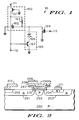
- FIG. 1 is a detailed schematic diagram illustrating an off-line bootstrap circuit 10 that includes a high voltage device 100, clamping circuit 105, and control transistor 109 for turning off device 100.
- the high voltage device 100 includes JFET transistor 101, NMOS transistor 102, and n-well resistor 103.
- the JFET transistor 101 is an n-channel, depletion mode JFET transistor with a source to backgate pinch-off voltage of approximately 50V.
- the backgate is connected to ground, the drain is connected to terminal 111 at which a line voltage is applied thereat, and the source is connected to the drain of NMOS transistor 102 and the first terminal of n-well resistor 103.
- the current through JFET transistor 101 is controlled by the NMOS transistor 102, and must be limited by the duty cycle of a control signal so as not to exceed the safe operating area of the JFET transistor 101.
- the current through JFET transistor 101 is controlled by the bias current through n-well resistor 103. This bias current must be small to minimize the power dissipated by device 100.
- the JFET transistor's body When a line voltage is applied to the drain of the JFET transistor 101, the JFET transistor's body is fully depleted with a typical source to substrate pinch-off voltage of 50V wherein the body of the JFET transistor is often referred to as the drift region of the high voltage device 100.
- the JFET transistor 101 is operated in its current saturation region. Since the source voltage of JFET 101 is limited to approximately 50V, most of the line voltage applied at terminal 111 is dropped across the body of the JFET transistor thereby providing a buffer from the line voltage. This protects the NMOS transistor 102 and n-well resistor 103 that are connected to this node.
- the NMOS transistor 102 is an n-channel enhancement mode MOS transistor with a threshold range of 1.5V.
- the drain of transistor 102 is connected to the source of JFET transistor 101 and a first terminal of n-well resistor 103.
- the source of transistor 102 is connected to terminal 112.
- the gate of transistor 102 is connected to a second terminal of n-well resistor 103, clamping circuit 105, and turn-off device 109.
- the backgate of transistor 102 is connected to ground.
- the drain voltage of transistor 102 is limited by JFET transistor 101.
- the source voltage of transistor 102 should be limited to approximately 50V by external circuitry (not shown) coupled to terminal 112.
- the gate voltage of transistor 102 is limited by the clamping circuit 105.
- Startup applications do not require tight control of the current through transistor 102.
- the startup current should generally be in the range of 5mA to 25mA as the voltage at the source of transistor 102 ramps from 0V to 20V. This can be accomplished without closed loop control.
- the gate voltage of transistor 102 should be as large as possible to minimize current variation due to backgate effects.
- the current amplitude is set by adjusting the channel length of NMOS transistor 102.
- the device design of NMOS transistor 102 will be discussed later with reference to FIG.'s 2 and 3.
- the n-well resistor 103 provides bias current to turn on NMOS transistor 102.
- the first terminal of the n-well resistor is connected to the drain of NMOS transistor 102, and the second terminal of the n-well resistor is connected to the gate of the NMOS transistor 102.
- the bias current is kept small since it is conducted from the line voltage through JFET transistor 101 after the high voltage device 100 is turned OFF.
- the narrow n-well resistor 103 has significant depletion effects which makes its electrical behavior more characteristic of a JFET than an ideal resistor. It is designed to supply approximately 25uA of bias current when the gate of the NMOS transistor 102 is at ground.
- the n-well resistor 103 is designed so that its pinch-off voltage is sufficiently high so as not to interfere with the function of the clamping circuit 105.
- Clamping circuit 105 limits the voltage appearing at the control electrode of transistor 102 thereby limiting the current flowing between terminals 111 and 112.
- Clamping circuit 105 includes an avalanche diode 106 having a typical breakdown voltage of 10V, and a PNP transistor 107.
- the cathode of the diode is connected to the gate of the NMOS transistor 102.
- the anode of the diode is connected to the emitter of the PNP transistor 107.
- the base of the PNP transistor is connected to the source of the NMOS transistor 102, and the collector of the PNP transistor is connected to ground reference.
- the clamping voltage is typically below 20V to prevent long term degradation of the gate oxide of the NMOS transistor 102.
- Clamping circuit 105 has a forward voltage of 11V.
- the 10V avalanche diode was selected for its low leakage, providing a sharp knee at low bias currents.
- clamping circuit 105 has a reverse blocking voltage in excess of 50V due to the high BV EBO voltage of the PNP transistor 107.
- the high voltage device 100 is turned OFF by pulling its control terminal to ground.
- This ON/OFF function can be implemented using a single pull-down control transistor 109.
- the source and backgate of transistor 109 is connected to ground.
- the drain of transistor 109 is connected to the control terminal of high voltage device 100.
- the gate of transistor 109 is coupled to terminal 113 at which a control signal is applied thereat.
- control transistor 109 When the control signal applied at terminal 113 is a logic low, control transistor 109 is OFF, and high voltage device 100 is ON and provides a high source to ground breakdown voltage between terminals 111 and 112 and also a high current between terminals 111 and 112. However, when the control signal applied at terminal 113 is a logic high, control transistor 109 pulls the control terminal of high voltage device 100 to ground thereby turning device 100 OFF thereby providing a high impedance between terminals 111 and 112. The breakdown voltage at the drain of control transistor 109 should exceed 30V so as not to interfere with the function of clamping circuit 105. Transistor 109 may take the form of a high voltage DMOS type transistor.
- the present invention provides an off-line start up circuit that includes a high voltage device.
- the high voltage device provides an initial current for increasing a voltage at a bias terminal. However, once the voltage appearing at the bias terminal reaches a predetermined threshold, the high voltage device is rendered non-operative.
- the high voltage device includes an NMOS transistor having a high source to ground breakdown voltage for extending a usable voltage range appearing at the bias terminal.
- the high voltage device 100 can be illustrated with two regions with each region differing in device operation. These two regions are merged into a complex but unified device structure.
- FIG.'s 2 and 3 are pictorial diagrams illustrating cross-section views showing these two regions of high voltage device 100.
- FIG. 2 shows a cross-section slicing through the transistors 101 and 102.
- FIG. 3 shows a cross-section slicing through the JFET transistor 101 and n-well resistor 103.
- the drawings are not shown to scale.
- the central drain contact region (212) includes the drain bonding pad. This closed geometry is a common way of using a bond wire to avoid running high voltage metal across the surface of the die.
- Figure 2 is a cross-section of high voltage device 100 in a region where the JFET transistor (101) is coupled to the NMOS transistor (102).
- the n-well region 201 is the body of the JFET transistor 101.
- the drain region of device 100 is on the left end of the body, and the source region of device 100 is on the right end.
- the substrate 200 serves as the backgate junction.
- the source of the JFET transistor 101 and the drain of the NMOS transistor 102 are merged so that no contact region is required, and there is no distinct boundary between the two transistors.
- the NMOS transistor 102 has a source region 203 with contact 204 and a metal electrode 211, a backgate p-well diffusion 202, and a silicon gate electrode 207 that is used to form channel 210 during conduction.
- the breakdown voltage at the drain of transistor 101 must exceed 400V for world-wide line voltage applications.
- the lengths of the drain metal field plate 212, the gate metal field plate 209, and n-well region 201 which forms the body of the JFET transistor are optimized for this particular breakdown voltage.
- the breakdown voltage at the source of transistor 102 must exceed 50V to support a wide bias supply voltage range. This is accomplished by using n-well as the source diffusion to provide high breakdown voltage relative to the substrate, and by spacing the source contact region 204 away from the channel to reduce the voltage drop across the gate oxide.
- the maximum sustained voltage across the thin gate oxide must be kept below 20V for long term reliability considerations.
- a worst case reverse bias occurs when both current carrying terminals (the drain of transistor 101 and source of transistor 102) of device 100 are at maximum voltage, and the control terminal of device 100 is grounded.
- the JFET drain edge of the n-well region 201 and the p-well backgate region 202 are spaced so that the depletion spread under reverse bias conditions greatly reduces the voltage across the gate oxide.
- the p-well region 202 sets the threshold voltage and also prevents punch through between drain and source regions 201 and 203.
- the backgate is inherently connected to ground through the substrate, which eliminates the parasitic drain-source diode and allows the drain voltage of device 100 to swing to ground.
- the n-well resistor (103) must be able to bias the gate electrode 207 up to 30V without pinching off. This is accomplished by keeping the p-well diffusion away from the body of the n-well resistor to minimize the depletion effects.
- Figure 3 is a cross-section of device (100) in the region where the source end of JFET transistor (101) is coupled to the "high" end of the N-well resistor (103).
- the N-well region 401 is the body of the JFET transistor 101 and corresponds to region 201 of FIG. 2.
- the drain contact is located on the left end of the body and the source end is the N-well region adjacent to the left edge of the gate electrode (406/207).
- the p- substrate 400 which corresponds to p-substrate 200 of FIG. 2 functions as the back gate of the JFET transistor.
- the source of the JFET transistor and the "high" side of the N-well resistor are merged and there is no distinct boundary between the two devices.
- the resistance of the N-well resistor is controlled by adjusting the distance between region 402 and the N-well resistor contact enhancement diffusion (403). Electrical contact to the "low" end of the N-well resistor 403 is provided by the N-well resistor contact (405).
- Region 404 consists of an insulating dielectric film electrically separating regions 401 and 406.
- the potential of the N-well in region 401 may be biased to up to a maximum of approximately 50V, while the electrode 406 may be at ground Region 404 is thick field oxide, so the resultant electric field applied across this oxide is very small resulting in a negligible effect on the long term reliability of the device.
- the silicon gate electrode (207/406) is utilized to form the conducting channel 210 of the NMOS transistor, but has no significant effect in this region of resistor 103 of device 100.
- the length of the gate metal field plate 407 is similar to plate 209 as aforedescribed.
- Prior art startup devices do not allow for large hysteresis in the UVLO Comparator thresholds, making the startup sequence more difficult.
- the startup technique described in US Patent #5,014,178, assigned to Power Integrations, Inc. and having an issue date of 5/7/91, teaches a method of interleaving the switching of the startup device and the switching device so that the startup device provides bias current to the control circuit during the OFF-time of the switching device.
- this requires the startup device to be switched at high frequency, typically in excess of 50kHz. This is generally not obtainable with the small currents involved in biasing the startup device.
- circuit 300 does not require high frequency switching of the bootstrap circuit 302.
- the bootstrap circuit 302 is turned ON only once and after a rectified line voltage is applied.
- the slow, controlled nature of the UVLO Comparator guarantees that there is no interference between the two high voltage devices that share the common high voltage pin.
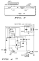
- Circuit 300 includes off-line bootstrap circuit 302, switching circuit 307 and 308, and under voltage lock out (UVLO) circuit 303.
- the off-line bootstrap circuit 302 which corresponds to bootstrap circuit 10 of FIG. 1, is coupled to a rectified line voltage through inductive load 305. Since the bootstrap circuit 302 conducts only a small continuous current, the voltage drop across inductive load 305 should be substantially equal to zero.
- High voltage terminal 111 of bootstrap circuit 302 is coupled to the high voltage drain electrode of switching transistor 308 to from a common connection thereat. This common connection couples the high voltage nodes of bootstrap circuit 302 and switching device 308 thereby allowing for one IC pin when both high voltage devices reside in the same package. In addition, it improves the ESD ruggedness of the physically small bootstrap circuit device.
- passgate 309 guarantees that while the bootstrap circuit 302 is ON, the switching device 308 is OFF.
- the UVLO Comparator 303 has a first input coupled to terminal 112 and a second input coupled to receive a threshold voltage V T .
- the output of comparator 303 is coupled to terminal 113 and to a first input of passgate gate 309.
- Comparator 303 has a large threshold hysteresis, with an upper threshold of typically 15V, and a lower threshold of typically 10V. The large hysteresis makes the bootstrap startup function easier to implement.
- the UVLO Comparator 303 controls the sequencing of events during the bootstrap startup period.
- a rectified line voltage is first applied to terminal 111 via inductive load 305, terminal 112 is at ground, below the upper threshold of UVLO Comparator 303, causing its output to be low.
- the output is coupled so that a low signal turns ON bootstrap circuit 302, and disables passgate 309, holding OFF switching device 308.
- the startup current supplied by bootstrap circuit 302 then ramps the voltage at terminal 112 to the upper threshold of UVLO Comparator 303, causing its output to go high.
- the output is coupled so that a high signal turns OFF bootstrap circuit 302, and enables passgate 309 so that the PWM circuit 307 controls the conduction of switching device 308.
- the present invention provides an off-line startup circuit for providing a wider bias voltage range to an integrated circuit.
- the startup circuit described is implemented on a high voltage integrated circuit (HVIC) technology that is optimized for low side switch applications.
- HVIC high voltage integrated circuit
- Previous startup circuits included a high voltage device that typically uses the same transistor design as the low side power switching device. This is normally implemented as an enhancement mode lateral DMOS transistor connected in series with a depletion mode lateral JFET transistor where the JFET transistor serves as the drift region of the high voltage device.
- the floating high voltage startup transistor is difficult to implement.
- the source to substrate breakdown voltage is limited to 10V to 15V.
- the backgate of the DMOS transistor is connected to its source and isolated from the substrate by extending the drain n-type well region underneath the p-type body region.
- the n-type well has a junction depth of approximately 5um, while the p-type body has a junction depth of approximately 2um.
- the typical breakdown voltage between the p-type body and the substrate is only 15V.
- the isolated DMOS transistor is substantially different from the grounded source transistor, requiring a different design for the drift length and field plates.
- a goal of the startup circuit of the present invention is to provide a high source voltage so as not to limit the supply voltage range of the integrated circuit it connects to wherein a small supply voltage range results in a need for tight regulation.
- the NMOS transistor described in FIG.'s 2 and 3 provides much higher breakdown voltage than can be achieved with DMOS type transistors.
- the NMOS transistor can be controlled with the simple circuit described in FIG. 1.
Abstract
Description
- This invention relates to startup circuits and, more particularly, to bootstrap startup circuits that are used in power supplies to initialize the bias voltage to integrated circuits.
- Generally, a bootstrap startup circuit provides an initial voltage across a capacitor prior to a power supply for the integrated circuit attaining its predetermined value. Further, the bootstrap startup circuit is turned off once the power supply attains its predetermined value.
- Typically, a bootstrap startup circuit may include a single resistor or a power up transistor circuit. However, a disadvantage of the single resistor bootstrap startup circuit is that it draws a significant amount of current, while a disadvantage of the integrated power up transistor bootstrap startup circuit is that the bias voltage range is limited to a maximum of approximately 10-15 volts. This limited bias voltage range may become a problem when a wider bias voltage range is needed such as when primary-side control integrated circuits have an input voltage range of 10-30 volts.
- Hence, there is a need for a bootstrap startup circuit that has a lower current drain and for providing a wide bias voltage range.
-
- FIG. 1 is a detailed schematic diagram illustrating an off-line bootstrap startup circuit in accordance with the present invention;
- FIG.'s 2 and 3 are detailed pictorial diagrams illustrating cross-section views of a high voltage device shown in FIG. 1; and
- FIG. 4 is a schematic/block diagram illustrating a circuit including the off-line bootstrap startup circuit of FIG. 1 for switching an inductive load.
- Generally, the present invention provides a circuit coupled to a line voltage for providing a wider bias voltage range to an integrated circuit. This is accomplished by using a technique known as bootstrapping. A high voltage startup device provides bias current to initialize the supply voltage to a control circuit. However, once the power supply of the integrated circuit reaches its predetermined value, the startup device is switched off to minimize power dissipation. Thus, the present invention describes a novel high voltage startup device that simplifies circuit design, increases the supply voltage range of the control circuit, and eliminates the need for a dedicated high voltage pin, if a power switching transistor is integrated in the same package.
- The present invention can be more fully described with reference to FIG.'s 1-4. FIG. 1 is a detailed schematic diagram illustrating an off-
line bootstrap circuit 10 that includes a high voltage device 100, clamping circuit 105, andcontrol transistor 109 for turning off device 100. - In a preferred embodiment, the high voltage device 100 includes
JFET transistor 101,NMOS transistor 102, and n-well resistor 103. TheJFET transistor 101 is an n-channel, depletion mode JFET transistor with a source to backgate pinch-off voltage of approximately 50V. The backgate is connected to ground, the drain is connected toterminal 111 at which a line voltage is applied thereat, and the source is connected to the drain ofNMOS transistor 102 and the first terminal of n-well resistor 103. - When device 100 is ON, the current through
JFET transistor 101 is controlled by theNMOS transistor 102, and must be limited by the duty cycle of a control signal so as not to exceed the safe operating area of theJFET transistor 101. When device 100 is OFF, the current throughJFET transistor 101 is controlled by the bias current through n-well resistor 103. This bias current must be small to minimize the power dissipated by device 100. - When a line voltage is applied to the drain of the
JFET transistor 101, the JFET transistor's body is fully depleted with a typical source to substrate pinch-off voltage of 50V wherein the body of the JFET transistor is often referred to as the drift region of the high voltage device 100. TheJFET transistor 101 is operated in its current saturation region. Since the source voltage ofJFET 101 is limited to approximately 50V, most of the line voltage applied atterminal 111 is dropped across the body of the JFET transistor thereby providing a buffer from the line voltage. This protects theNMOS transistor 102 and n-well resistor 103 that are connected to this node. - The
NMOS transistor 102 is an n-channel enhancement mode MOS transistor with a threshold range of 1.5V. The drain oftransistor 102 is connected to the source ofJFET transistor 101 and a first terminal of n-well resistor 103. The source oftransistor 102 is connected toterminal 112. The gate oftransistor 102 is connected to a second terminal of n-well resistor 103, clamping circuit 105, and turn-offdevice 109. The backgate oftransistor 102 is connected to ground. - The drain voltage of
transistor 102 is limited byJFET transistor 101. The source voltage oftransistor 102 should be limited to approximately 50V by external circuitry (not shown) coupled toterminal 112. The gate voltage oftransistor 102 is limited by the clamping circuit 105. Startup applications do not require tight control of the current throughtransistor 102. The startup current should generally be in the range of 5mA to 25mA as the voltage at the source oftransistor 102 ramps from 0V to 20V. This can be accomplished without closed loop control. The gate voltage oftransistor 102 should be as large as possible to minimize current variation due to backgate effects. The current amplitude is set by adjusting the channel length ofNMOS transistor 102. The device design ofNMOS transistor 102 will be discussed later with reference to FIG.'s 2 and 3. - The n-
well resistor 103 provides bias current to turn onNMOS transistor 102. To minimize the resistors value and its physical layout, the first terminal of the n-well resistor is connected to the drain ofNMOS transistor 102, and the second terminal of the n-well resistor is connected to the gate of theNMOS transistor 102. The bias current is kept small since it is conducted from the line voltage throughJFET transistor 101 after the high voltage device 100 is turned OFF. The narrow n-well resistor 103 has significant depletion effects which makes its electrical behavior more characteristic of a JFET than an ideal resistor. It is designed to supply approximately 25uA of bias current when the gate of theNMOS transistor 102 is at ground. The n-well resistor 103 is designed so that its pinch-off voltage is sufficiently high so as not to interfere with the function of the clamping circuit 105. - Clamping circuit 105 limits the voltage appearing at the control electrode of
transistor 102 thereby limiting the current flowing betweenterminals avalanche diode 106 having a typical breakdown voltage of 10V, and aPNP transistor 107. The cathode of the diode is connected to the gate of theNMOS transistor 102. The anode of the diode is connected to the emitter of thePNP transistor 107. The base of the PNP transistor is connected to the source of theNMOS transistor 102, and the collector of the PNP transistor is connected to ground reference. - The clamping voltage is typically below 20V to prevent long term degradation of the gate oxide of the
NMOS transistor 102. Clamping circuit 105 has a forward voltage of 11V. The 10V avalanche diode was selected for its low leakage, providing a sharp knee at low bias currents. To simplify the design of the ON/OFF control function, it is desirable to allow the gate of theNMOS transistor 102 to be pulled to ground, yet allow the source of theNMOS transistor 102 to exceed 50V. Thus, clamping circuit 105 has a reverse blocking voltage in excess of 50V due to the high BVEBO voltage of thePNP transistor 107. - The high voltage device 100 is turned OFF by pulling its control terminal to ground. This ON/OFF function can be implemented using a single pull-
down control transistor 109. The source and backgate oftransistor 109 is connected to ground. The drain oftransistor 109 is connected to the control terminal of high voltage device 100. The gate oftransistor 109 is coupled toterminal 113 at which a control signal is applied thereat. - When the control signal applied at
terminal 113 is a logic low,control transistor 109 is OFF, and high voltage device 100 is ON and provides a high source to ground breakdown voltage betweenterminals terminals terminal 113 is a logic high,control transistor 109 pulls the control terminal of high voltage device 100 to ground thereby turning device 100 OFF thereby providing a high impedance betweenterminals control transistor 109 should exceed 30V so as not to interfere with the function of clamping circuit 105.Transistor 109 may take the form of a high voltage DMOS type transistor. - In summary, the present invention provides an off-line start up circuit that includes a high voltage device. The high voltage device provides an initial current for increasing a voltage at a bias terminal. However, once the voltage appearing at the bias terminal reaches a predetermined threshold, the high voltage device is rendered non-operative. The high voltage device includes an NMOS transistor having a high source to ground breakdown voltage for extending a usable voltage range appearing at the bias terminal.
- The high voltage device 100 can be illustrated with two regions with each region differing in device operation. These two regions are merged into a complex but unified device structure. FIG.'s 2 and 3 are pictorial diagrams illustrating cross-section views showing these two regions of high voltage device 100. FIG. 2 shows a cross-section slicing through the
transistors JFET transistor 101 and n-well resistor 103. For clarity, the drawings are not shown to scale. - The central drain contact region (212) includes the drain bonding pad. This closed geometry is a common way of using a bond wire to avoid running high voltage metal across the surface of the die. Figure 2 is a cross-section of high voltage device 100 in a region where the JFET transistor (101) is coupled to the NMOS transistor (102). The n-
well region 201 is the body of theJFET transistor 101. The drain region of device 100 is on the left end of the body, and the source region of device 100 is on the right end. Thesubstrate 200 serves as the backgate junction. The source of theJFET transistor 101 and the drain of theNMOS transistor 102 are merged so that no contact region is required, and there is no distinct boundary between the two transistors. TheNMOS transistor 102 has asource region 203 with contact 204 and ametal electrode 211, a backgate p-well diffusion 202, and asilicon gate electrode 207 that is used to formchannel 210 during conduction. - The breakdown voltage at the drain of
transistor 101 must exceed 400V for world-wide line voltage applications. The lengths of the drainmetal field plate 212, the gatemetal field plate 209, and n-well region 201 which forms the body of the JFET transistor are optimized for this particular breakdown voltage. The breakdown voltage at the source oftransistor 102 must exceed 50V to support a wide bias supply voltage range. This is accomplished by using n-well as the source diffusion to provide high breakdown voltage relative to the substrate, and by spacing the source contact region 204 away from the channel to reduce the voltage drop across the gate oxide. The maximum sustained voltage across the thin gate oxide must be kept below 20V for long term reliability considerations. - A worst case reverse bias occurs when both current carrying terminals (the drain of
transistor 101 and source of transistor 102) of device 100 are at maximum voltage, and the control terminal of device 100 is grounded. The JFET drain edge of the n-well region 201 and the p-wellbackgate region 202 are spaced so that the depletion spread under reverse bias conditions greatly reduces the voltage across the gate oxide. The p-well region 202 sets the threshold voltage and also prevents punch through between drain andsource regions gate electrode 207 up to 30V without pinching off. This is accomplished by keeping the p-well diffusion away from the body of the n-well resistor to minimize the depletion effects. - Figure 3 is a cross-section of device (100) in the region where the source end of JFET transistor (101) is coupled to the "high" end of the N-well resistor (103). The N-
well region 401 is the body of theJFET transistor 101 and corresponds toregion 201 of FIG. 2. The drain contact is located on the left end of the body and the source end is the N-well region adjacent to the left edge of the gate electrode (406/207). The p-substrate 400 which corresponds to p-substrate 200 of FIG. 2 functions as the back gate of the JFET transistor. The source of the JFET transistor and the "high" side of the N-well resistor are merged and there is no distinct boundary between the two devices. The resistance of the N-well resistor is controlled by adjusting the distance betweenregion 402 and the N-well resistor contact enhancement diffusion (403). Electrical contact to the "low" end of the N-well resistor 403 is provided by the N-well resistor contact (405).Region 404 consists of an insulating dielectric film electrically separatingregions - The potential of the N-well in
region 401 may be biased to up to a maximum of approximately 50V, while theelectrode 406 may be atground Region 404 is thick field oxide, so the resultant electric field applied across this oxide is very small resulting in a negligible effect on the long term reliability of the device. - The silicon gate electrode (207/406) is utilized to form the conducting
channel 210 of the NMOS transistor, but has no significant effect in this region ofresistor 103 of device 100. The length of the gatemetal field plate 407 is similar toplate 209 as aforedescribed. - Prior art startup devices do not allow for large hysteresis in the UVLO Comparator thresholds, making the startup sequence more difficult. The startup technique described in US Patent #5,014,178, assigned to Power Integrations, Inc. and having an issue date of 5/7/91, teaches a method of interleaving the switching of the startup device and the switching device so that the startup device provides bias current to the control circuit during the OFF-time of the switching device. However, this requires the startup device to be switched at high frequency, typically in excess of 50kHz. This is generally not obtainable with the small currents involved in biasing the startup device.
- However, referring to FIG. 4, which illustrates
circuit 300 including the bootstrap circuit shown in FIG. 1 for switchinginductive load 305,circuit 300 does not require high frequency switching of thebootstrap circuit 302. During normal operation, thebootstrap circuit 302 is turned ON only once and after a rectified line voltage is applied. The slow, controlled nature of the UVLO Comparator guarantees that there is no interference between the two high voltage devices that share the common high voltage pin. There is generally a deadtime between when the bootstrap circuit is turned OFF, and when the switching device is turned ON. This deadtime provides time for the analog portion of the control circuit to switch from a sleep mode to an awake mode. -
Circuit 300 includes off-line bootstrap circuit 302, switchingcircuit circuit 303. The off-line bootstrap circuit 302, which corresponds to bootstrapcircuit 10 of FIG. 1, is coupled to a rectified line voltage throughinductive load 305. Since thebootstrap circuit 302 conducts only a small continuous current, the voltage drop acrossinductive load 305 should be substantially equal to zero.High voltage terminal 111 ofbootstrap circuit 302 is coupled to the high voltage drain electrode of switchingtransistor 308 to from a common connection thereat. This common connection couples the high voltage nodes ofbootstrap circuit 302 and switchingdevice 308 thereby allowing for one IC pin when both high voltage devices reside in the same package. In addition, it improves the ESD ruggedness of the physically small bootstrap circuit device. - Since the high voltage terminals of
bootstrap circuit 302 and switchingdevice 308 are coupled to the same node, they must not be allowed to conduct at the same time or else thebias terminal 112 will be discharged. Therefore,passgate 309 guarantees that while thebootstrap circuit 302 is ON, theswitching device 308 is OFF. - The
UVLO Comparator 303 has a first input coupled toterminal 112 and a second input coupled to receive a threshold voltage VT. The output ofcomparator 303 is coupled toterminal 113 and to a first input ofpassgate gate 309.Comparator 303 has a large threshold hysteresis, with an upper threshold of typically 15V, and a lower threshold of typically 10V. The large hysteresis makes the bootstrap startup function easier to implement. - The
UVLO Comparator 303 controls the sequencing of events during the bootstrap startup period. When a rectified line voltage is first applied toterminal 111 viainductive load 305, terminal 112 is at ground, below the upper threshold ofUVLO Comparator 303, causing its output to be low. The output is coupled so that a low signal turns ONbootstrap circuit 302, and disablespassgate 309, holding OFF switchingdevice 308. The startup current supplied bybootstrap circuit 302 then ramps the voltage atterminal 112 to the upper threshold ofUVLO Comparator 303, causing its output to go high. The output is coupled so that a high signal turns OFFbootstrap circuit 302, and enablespassgate 309 so that thePWM circuit 307 controls the conduction of switchingdevice 308. It normally takes several switching cycles before thepower supply 306 can deliver bias current to thePWM control circuit 307. There may be additional delay due to the soft start function within the PWM circuit. During this conduction dead band, the bias current to thePWM circuit 307 is supplied by thebypass capacitor 310.Capacitor 310 must be large enough so that the voltage atterminal 112 does not drop below the lower threshold of theUVLO comparator 303. If this happens, the startup sequence is re-initiated. - The present invention provides an off-line startup circuit for providing a wider bias voltage range to an integrated circuit. The startup circuit described is implemented on a high voltage integrated circuit (HVIC) technology that is optimized for low side switch applications.
- Previous startup circuits included a high voltage device that typically uses the same transistor design as the low side power switching device. This is normally implemented as an enhancement mode lateral DMOS transistor connected in series with a depletion mode lateral JFET transistor where the JFET transistor serves as the drift region of the high voltage device. However, because the technology is designed for grounded source switching applications, the floating high voltage startup transistor is difficult to implement.
- In a DMOS type transistor, the source to substrate breakdown voltage is limited to 10V to 15V. For maximum breakdown voltage, the backgate of the DMOS transistor is connected to its source and isolated from the substrate by extending the drain n-type well region underneath the p-type body region. The n-type well has a junction depth of approximately 5um, while the p-type body has a junction depth of approximately 2um. However, because the n-type isolating layer is so thin and lightly doped, the typical breakdown voltage between the p-type body and the substrate is only 15V. In addition, the isolated DMOS transistor is substantially different from the grounded source transistor, requiring a different design for the drift length and field plates.
- An alternate technique that uses the grounded backgate design of the standard switching transistor which allows the drain to swing below the source without forward biasing the parasitic drain-body diode. This further reduces the source to substrate breakdown voltage to typically 10V.
- However, a goal of the startup circuit of the present invention is to provide a high source voltage so as not to limit the supply voltage range of the integrated circuit it connects to wherein a small supply voltage range results in a need for tight regulation. The NMOS transistor described in FIG.'s 2 and 3 provides much higher breakdown voltage than can be achieved with DMOS type transistors. The NMOS transistor can be controlled with the simple circuit described in FIG. 1.
- While the invention has been described in specific embodiments thereof, it is evident that many alterations, modifications and variations will be apparent to those skilled in the art. Further, it is intended to embrace all such alterations, modifications and variations in the appended claims.
Claims (9)
- An off-line bootstrap circuit being responsive to a line voltage for providing a bias voltage to an integrated circuit, the off-line bootstrap circuit comprising:
a high voltage device (100) having first and second current carrying terminals and a control terminal, said first current carrying terminal of said high voltage device being coupled for receiving the line voltage, said second current carrying terminal of said high voltage device being coupled for providing the bias voltage, said high voltage device including a first transistor (101) for extending a range of the bias voltage;
clamping means (105) coupled to said control terminal of said high voltage device for limiting voltage appearing thereat; and
control means (109) coupled to said control terminal of said high voltage device and responsive to a control signal for rendering said high voltage device inoperative when the bias voltage has exceeded a predetermined threshold. - The off-line bootstrap circuit according to claim 1 wherein said first transistor is an N-channel enhancement mode transistor.
- The off-line bootstrap circuit according to claim 1 wherein said first transistor includes N-well source and drain regions.
- The off-line bootstrap circuit according to claim 1 wherein said high voltage device includes:
said first transistor (102) having first and second current carrying electrodes, a control electrode and a back gate electrode, said second current carrying electrode of said first transistor coupled for providing the bias voltage, said control electrode of said first transistor coupled to said clamping means and to said control means, said back gate electrode of said first transistor coupled to a first supply voltage terminal; and
a second transistor (101) having first and second current carrying electrodes and a control electrode, said first current carrying electrode of said second transistor coupled for receiving the line voltage, said second current carrying electrode of said second transistor coupled to said first current carrying electrode of said first transistor, said control electrode of said second transistor coupled to said first supply voltage terminal wherein said first current carrying electrode of said first transistor is merged in a common region with said second current carrying electrode of said second transistor. - The off-line bootstrap circuit according to claim 4 wherein said high voltage device further includes a resistor (103) having first and second terminals respectively coupled to said second current carrying electrode of said second transistor and said control electrode of said first transistor, wherein said second current carrying electrode of said second transistor is merged in a common region with said first terminal of said resistor.
- The off-line bootstrap circuit according to claim 5 wherein said resistor is separated from said control terminal of said first transistor by a dielectric.
- The off-line bootstrap circuit according to claim 1 wherein said clamping means includes:
a transistor (107) having first and second current carrying electrodes and a control electrode, said first current carrying electrode of said transistor coupled to a first supply voltage terminal, said control electrode of said transistor coupled to said second terminal of said high voltage device; and
a diode (106) coupled between said control terminal of said high voltage device and said second current carrying terminal of said transistor. - The off-line bootstrap circuit according to claim 1 wherein said control means includes a transistor (109) having first and second current carrying electrodes and a control electrode, said first current carrying electrode of said transistor coupled to said control terminal of said high voltage device, said second current carrying electrode of said transistor coupled to a first supply voltage terminal, said control electrode of said transistor coupled for receiving said control signal.
- A method for utilizing a line voltage applied at a first terminal to provide a wider bias voltage range at a second terminal, the method comprising the steps of:
buffering the line voltage;
providing a high breakdown voltage between the second terminal and a first supply voltage terminal when a voltage appearing at the second terminal is below a predetermined threshold thereby extending a voltage range at the second terminal;
clamping a current flowing between the first and second terminals; and
providing a high impedance between the first and second terminals when said voltage appearing at the second terminal has exceeded said predetermined threshold.
Applications Claiming Priority (2)
| Application Number | Priority Date | Filing Date | Title |
|---|---|---|---|
| US08/140,944 US5477175A (en) | 1993-10-25 | 1993-10-25 | Off-line bootstrap startup circuit |
| US140944 | 1993-10-25 |
Publications (2)
| Publication Number | Publication Date |
|---|---|
| EP0650111A2 true EP0650111A2 (en) | 1995-04-26 |
| EP0650111A3 EP0650111A3 (en) | 1997-07-16 |
Family
ID=22493484
Family Applications (1)
| Application Number | Title | Priority Date | Filing Date |
|---|---|---|---|
| EP94115952A Ceased EP0650111A3 (en) | 1993-10-25 | 1994-10-10 | Off-line bootstrap startup circuit. |
Country Status (3)
| Country | Link |
|---|---|
| US (1) | US5477175A (en) |
| EP (1) | EP0650111A3 (en) |
| JP (1) | JPH07236229A (en) |
Cited By (4)
| Publication number | Priority date | Publication date | Assignee | Title |
|---|---|---|---|---|
| EP1843470A1 (en) * | 2003-10-14 | 2007-10-10 | Semiconductor Components Industries, LLC | Power system inhibit method and device and structure therefor |
| CN104362149A (en) * | 2014-09-18 | 2015-02-18 | 成都星芯微电子科技有限公司 | Semiconductor starting device based on spiral polycrystalline silicon field effect transistor charging and manufacturing process of semiconductor starting device |
| CN108347181A (en) * | 2017-01-25 | 2018-07-31 | 王俊杰 | A kind of power supply change-over device |
| CN109478079A (en) * | 2016-10-13 | 2019-03-15 | 惠普发展公司,有限责任合伙企业 | Switch for feed-through capacitor |
Families Citing this family (48)
| Publication number | Priority date | Publication date | Assignee | Title |
|---|---|---|---|---|
| US5640317A (en) * | 1995-06-15 | 1997-06-17 | Supertax, Inc. | High voltage start-up circuit and method therefor |
| DE19920306B4 (en) * | 1999-05-03 | 2008-02-28 | Stmicroelectronics Gmbh | Circuit device for controlling the current through an inductive load |
| US6310789B1 (en) * | 1999-06-25 | 2001-10-30 | The Procter & Gamble Company | Dynamically-controlled, intrinsically regulated charge pump power converter |
| JP3236587B2 (en) * | 1999-09-30 | 2001-12-10 | 長野日本無線株式会社 | Switching power supply |
| US6775164B2 (en) | 2002-03-14 | 2004-08-10 | Tyco Electronics Corporation | Three-terminal, low voltage pulse width modulation controller IC |
| IL153606A0 (en) * | 2002-12-24 | 2003-07-06 | Lightech Electronics Ind Ltd | Energy saving startup circuit for power supply |
| KR101045197B1 (en) | 2003-10-14 | 2011-06-30 | 세미컨덕터 콤포넨츠 인더스트리즈 엘엘씨 | Power system inhibit method and device and structure therefor |
| US6940320B2 (en) | 2003-10-14 | 2005-09-06 | Semiconductor Components Industries, L.L.C. | Power control system startup method and circuit |
| EP1557560B1 (en) * | 2004-01-22 | 2007-10-17 | STMicroelectronics S.r.l. | Circuit for dynamic control of a power transistor in applications for high voltage |
| DE102005037409A1 (en) * | 2004-08-09 | 2006-03-30 | International Rectifier Corp., El Segundo | Start-up switch to provide a start-up voltage to an application circuit |
| US7306999B2 (en) * | 2005-01-25 | 2007-12-11 | Semiconductor Components Industries, L.L.C. | High voltage sensor device and method therefor |
| US7955943B2 (en) * | 2005-01-25 | 2011-06-07 | Semiconductor Components Industries, Llc | High voltage sensor device and method therefor |
| US7477532B2 (en) | 2005-08-18 | 2009-01-13 | Semiconductor Components Industries, L.L.C. | Method of forming a start-up device and structure therefor |
| JP5343306B2 (en) * | 2006-03-24 | 2013-11-13 | 富士電機株式会社 | IC for switching power supply and switching power supply |
| JP5564749B2 (en) * | 2006-11-20 | 2014-08-06 | 富士電機株式会社 | Semiconductor device, semiconductor integrated circuit, control IC for switching power supply, and switching power supply device |
| US9197132B2 (en) | 2006-12-01 | 2015-11-24 | Flextronics International Usa, Inc. | Power converter with an adaptive controller and method of operating the same |
| US7468649B2 (en) | 2007-03-14 | 2008-12-23 | Flextronics International Usa, Inc. | Isolated power converter |
| WO2010056989A1 (en) | 2008-11-14 | 2010-05-20 | Flextronics International Usa, Inc. | Driver for a synchronous rectifier and power converter employing the same |
| US9088216B2 (en) | 2009-01-19 | 2015-07-21 | Power Systems Technologies, Ltd. | Controller for a synchronous rectifier switch |
| US8520414B2 (en) | 2009-01-19 | 2013-08-27 | Power Systems Technologies, Ltd. | Controller for a power converter |
| US9019061B2 (en) | 2009-03-31 | 2015-04-28 | Power Systems Technologies, Ltd. | Magnetic device formed with U-shaped core pieces and power converter employing the same |
| US9000745B2 (en) * | 2009-04-10 | 2015-04-07 | Taiwan Semiconductor Manufacturing Company, Ltd. | Switching regulator and method for operating the same |
| US8618784B2 (en) * | 2009-04-10 | 2013-12-31 | Taiwan Semiconductor Manufacturing Company, Ltd. | Regulator control circuits, switching regulators, systems, and methods for operating switching regulators |
| US8169801B2 (en) * | 2009-05-28 | 2012-05-01 | Monolithic Power Systems, Inc. | Voltage converters with integrated low power leaker device and associated methods |
| JP5499915B2 (en) * | 2009-06-10 | 2014-05-21 | 富士電機株式会社 | High voltage semiconductor device |
| US8514593B2 (en) | 2009-06-17 | 2013-08-20 | Power Systems Technologies, Ltd. | Power converter employing a variable switching frequency and a magnetic device with a non-uniform gap |
| US9077248B2 (en) | 2009-06-17 | 2015-07-07 | Power Systems Technologies Ltd | Start-up circuit for a power adapter |
| US8643222B2 (en) | 2009-06-17 | 2014-02-04 | Power Systems Technologies Ltd | Power adapter employing a power reducer |
| US8638578B2 (en) | 2009-08-14 | 2014-01-28 | Power System Technologies, Ltd. | Power converter including a charge pump employable in a power adapter |
| JP5467454B2 (en) * | 2009-09-01 | 2014-04-09 | Nltテクノロジー株式会社 | Bootstrap circuit, level shift circuit, and word line drive circuit |
| US8976549B2 (en) | 2009-12-03 | 2015-03-10 | Power Systems Technologies, Ltd. | Startup circuit including first and second Schmitt triggers and power converter employing the same |
| US8520420B2 (en) | 2009-12-18 | 2013-08-27 | Power Systems Technologies, Ltd. | Controller for modifying dead time between switches in a power converter |
| US8787043B2 (en) | 2010-01-22 | 2014-07-22 | Power Systems Technologies, Ltd. | Controller for a power converter and method of operating the same |
| US9246391B2 (en) | 2010-01-22 | 2016-01-26 | Power Systems Technologies Ltd. | Controller for providing a corrected signal to a sensed peak current through a circuit element of a power converter |
| CN102870320B (en) | 2010-03-17 | 2016-11-02 | 电力系统技术有限公司 | The control system of power converter and operational approach thereof |
| JP5589827B2 (en) * | 2010-12-24 | 2014-09-17 | サンケン電気株式会社 | Start-up circuit, switching power supply IC and switching power supply device |
| US8792257B2 (en) | 2011-03-25 | 2014-07-29 | Power Systems Technologies, Ltd. | Power converter with reduced power dissipation |
| US9048747B2 (en) * | 2011-11-23 | 2015-06-02 | Zahid Ansari | Switched-mode power supply startup circuit, method, and system incorporating same |
| US8792256B2 (en) | 2012-01-27 | 2014-07-29 | Power Systems Technologies Ltd. | Controller for a switch and method of operating the same |
| US9190898B2 (en) | 2012-07-06 | 2015-11-17 | Power Systems Technologies, Ltd | Controller for a power converter and method of operating the same |
| US9214264B2 (en) | 2012-07-16 | 2015-12-15 | Power Systems Technologies, Ltd. | Magnetic device and power converter employing the same |
| US9099232B2 (en) | 2012-07-16 | 2015-08-04 | Power Systems Technologies Ltd. | Magnetic device and power converter employing the same |
| US9106130B2 (en) | 2012-07-16 | 2015-08-11 | Power Systems Technologies, Inc. | Magnetic device and power converter employing the same |
| US9379629B2 (en) | 2012-07-16 | 2016-06-28 | Power Systems Technologies, Ltd. | Magnetic device and power converter employing the same |
| US9240712B2 (en) | 2012-12-13 | 2016-01-19 | Power Systems Technologies Ltd. | Controller including a common current-sense device for power switches of a power converter |
| US9300206B2 (en) | 2013-11-15 | 2016-03-29 | Power Systems Technologies Ltd. | Method for estimating power of a power converter |
| CN106329959B (en) * | 2015-06-30 | 2019-04-26 | 华润矽威科技(上海)有限公司 | High pressure self-powered circuit |
| KR102107883B1 (en) | 2017-12-21 | 2020-05-08 | 매그나칩 반도체 유한회사 | High voltage start-up circuit for zeroing of standby power consumption and switching mode power supply having the same |
Citations (4)
| Publication number | Priority date | Publication date | Assignee | Title |
|---|---|---|---|---|
| US4811075A (en) * | 1987-04-24 | 1989-03-07 | Power Integrations, Inc. | High voltage MOS transistors |
| US5014178A (en) * | 1990-05-14 | 1991-05-07 | Power Integrations, Inc. | Self powering technique for integrated switched mode power supply |
| US5189600A (en) * | 1991-12-19 | 1993-02-23 | North American Philips Corporation | Combined power supply for main and stand-by power |
| EP0585788A1 (en) * | 1992-09-01 | 1994-03-09 | Power Integrations, Inc. | Switched mode power supply integrated circuit with start-up self-biasing |
Family Cites Families (5)
| Publication number | Priority date | Publication date | Assignee | Title |
|---|---|---|---|---|
| DE3632746C2 (en) * | 1986-09-26 | 1995-04-13 | Kommunikations Elektronik | Circuit arrangement for generating an AC voltage |
| US5051611A (en) * | 1989-12-20 | 1991-09-24 | Quadic Systems, Inc. | Power-up circuit with hysteresis for an output buffer |
| US5111070A (en) * | 1991-01-18 | 1992-05-05 | Allen-Bradley Company, Inc. | DC input circuit with controlled leakage current |
| JPH04285465A (en) * | 1991-03-13 | 1992-10-09 | Nec Corp | Switching power source with protective circuit |
| US5313381A (en) * | 1992-09-01 | 1994-05-17 | Power Integrations, Inc. | Three-terminal switched mode power supply integrated circuit |
-
1993
- 1993-10-25 US US08/140,944 patent/US5477175A/en not_active Expired - Lifetime
-
1994
- 1994-10-07 JP JP6270327A patent/JPH07236229A/en active Pending
- 1994-10-10 EP EP94115952A patent/EP0650111A3/en not_active Ceased
Patent Citations (4)
| Publication number | Priority date | Publication date | Assignee | Title |
|---|---|---|---|---|
| US4811075A (en) * | 1987-04-24 | 1989-03-07 | Power Integrations, Inc. | High voltage MOS transistors |
| US5014178A (en) * | 1990-05-14 | 1991-05-07 | Power Integrations, Inc. | Self powering technique for integrated switched mode power supply |
| US5189600A (en) * | 1991-12-19 | 1993-02-23 | North American Philips Corporation | Combined power supply for main and stand-by power |
| EP0585788A1 (en) * | 1992-09-01 | 1994-03-09 | Power Integrations, Inc. | Switched mode power supply integrated circuit with start-up self-biasing |
Non-Patent Citations (1)
| Title |
|---|
| IBM TECHNICAL DISCLOSURE BULLETIN, vol. 31, no. 5, October 1988, page 424/425 XP000023170 "LOW LOSS-TYPE STARTER CIRCUIT FOR SWITCHING MODE POWER SUPPLY" * |
Cited By (5)
| Publication number | Priority date | Publication date | Assignee | Title |
|---|---|---|---|---|
| EP1843470A1 (en) * | 2003-10-14 | 2007-10-10 | Semiconductor Components Industries, LLC | Power system inhibit method and device and structure therefor |
| CN104362149A (en) * | 2014-09-18 | 2015-02-18 | 成都星芯微电子科技有限公司 | Semiconductor starting device based on spiral polycrystalline silicon field effect transistor charging and manufacturing process of semiconductor starting device |
| CN109478079A (en) * | 2016-10-13 | 2019-03-15 | 惠普发展公司,有限责任合伙企业 | Switch for feed-through capacitor |
| CN108347181A (en) * | 2017-01-25 | 2018-07-31 | 王俊杰 | A kind of power supply change-over device |
| CN108347181B (en) * | 2017-01-25 | 2020-02-07 | 芯好半导体(成都)有限公司 | Power supply conversion device |
Also Published As
| Publication number | Publication date |
|---|---|
| US5477175A (en) | 1995-12-19 |
| JPH07236229A (en) | 1995-09-05 |
| EP0650111A3 (en) | 1997-07-16 |
Similar Documents
| Publication | Publication Date | Title |
|---|---|---|
| US5477175A (en) | Off-line bootstrap startup circuit | |
| JP4600180B2 (en) | Semiconductor circuit using field effect type power semiconductor element | |
| US4492883A (en) | Unpowered fast gate turn-off FET | |
| US6628159B2 (en) | SOI voltage-tolerant body-coupled pass transistor | |
| US5543650A (en) | Electrostatic discharge protection circuit employing a mosfet device | |
| EP2045920A1 (en) | Switching circuit having low threshold voltage | |
| EP0590895A2 (en) | Bi-directional MOSFET switch | |
| EP0562776B1 (en) | Driver circuit for sinking current to two supply voltages | |
| JP2007215389A (en) | Power semiconductor element and semiconductor circuit using same | |
| US6657274B2 (en) | Apparatus for controlling a high voltage circuit using a low voltage circuit | |
| US5801573A (en) | Protected switch having a power semiconductor device | |
| US8605399B2 (en) | Load driving device | |
| US20060044051A1 (en) | Bootstrap diode emulator with dynamic back-gate biasing and short-circuit protection | |
| US4908551A (en) | DC/AC bridge circuit | |
| US10886909B2 (en) | Electric assembly including an insulated gate bipolar transistor device and a wide-bandgap transistor device | |
| JPH07506941A (en) | Majority carrier power diode | |
| JPH10233632A (en) | High voltage side mosfet gate protection shunt circuit | |
| US4811191A (en) | CMOS rectifier circuit | |
| US6778366B2 (en) | Current limiting protection circuit | |
| US5475329A (en) | Turn-off circuit to provide a discharge path from a first node to a second node | |
| JPS62231518A (en) | High speed switch-off circuit of conductivity modulated field effect transistor | |
| JP3537061B2 (en) | Semiconductor device | |
| US5466952A (en) | Semiconductor device having an IGET and a control or protection component | |
| US6385025B2 (en) | Insulated gate type semiconductor apparatus with a control circuit | |
| US20050072990A1 (en) | Semiconductor device and driving circuit for semiconductor device |
Legal Events
| Date | Code | Title | Description |
|---|---|---|---|
| PUAI | Public reference made under article 153(3) epc to a published international application that has entered the european phase |
Free format text: ORIGINAL CODE: 0009012 |
|
| AK | Designated contracting states |
Kind code of ref document: A2 Designated state(s): DE FR GB |
|
| PUAL | Search report despatched |
Free format text: ORIGINAL CODE: 0009013 |
|
| AK | Designated contracting states |
Kind code of ref document: A3 Designated state(s): DE FR GB |
|
| 17P | Request for examination filed |
Effective date: 19980116 |
|
| 17Q | First examination report despatched |
Effective date: 19991224 |
|
| GRAG | Despatch of communication of intention to grant |
Free format text: ORIGINAL CODE: EPIDOS AGRA |
|
| STAA | Information on the status of an ep patent application or granted ep patent |
Free format text: STATUS: THE APPLICATION HAS BEEN REFUSED |
|
| 18R | Application refused |
Effective date: 20010924 |