EP0647070A2 - Verbesserungen für digitales Fernsehen - Google Patents
Verbesserungen für digitales Fernsehen Download PDFInfo
- Publication number
- EP0647070A2 EP0647070A2 EP94115121A EP94115121A EP0647070A2 EP 0647070 A2 EP0647070 A2 EP 0647070A2 EP 94115121 A EP94115121 A EP 94115121A EP 94115121 A EP94115121 A EP 94115121A EP 0647070 A2 EP0647070 A2 EP 0647070A2
- Authority
- EP
- European Patent Office
- Prior art keywords
- chrominance
- samples
- sampling
- luminance
- data
- Prior art date
- Legal status (The legal status is an assumption and is not a legal conclusion. Google has not performed a legal analysis and makes no representation as to the accuracy of the status listed.)
- Granted
Links
Images
Classifications
-
- H—ELECTRICITY
- H04—ELECTRIC COMMUNICATION TECHNIQUE
- H04N—PICTORIAL COMMUNICATION, e.g. TELEVISION
- H04N9/00—Details of colour television systems
- H04N9/77—Circuits for processing the brightness signal and the chrominance signal relative to each other, e.g. adjusting the phase of the brightness signal relative to the colour signal, correcting differential gain or differential phase
- H04N9/78—Circuits for processing the brightness signal and the chrominance signal relative to each other, e.g. adjusting the phase of the brightness signal relative to the colour signal, correcting differential gain or differential phase for separating the brightness signal or the chrominance signal from the colour television signal, e.g. using comb filter
Definitions
- This invention relates to television receivers, and more particularly to sampling an input video signal to obtain pixel data for varying display formats.
- sampling rate that is some multiple of the 3.58 MHz subcarrier frequency.
- a commonly used sampling rate is approximately 14.318 MHz, referred to as the "4 fsc" rate. It results in approximately 763 samples of active video data per line.
- a problem with the 4 fsc sampling rate is that it is not always consistent with the sampling rate required for a desired number of pixels per line (horizontal resolution). For example, today's enhanced definition television systems, such as "wide NTSC", call for an image that is wider than previous images, with an aspect ratio of 16:9. The desired aspect ratio and the available number of lines per frame determine the horizontal resolution.
- sampling rates for NTSC color separation and for a desired aspect ratio are not the same.
- 640 pixels per line are required.
- the 4 fsc sampling rate for NTSC color separation results in 763 samples per line. This requires some sort of means for providing samples for the desired horizontal resolution.
- Some existing systems provide the required number of pixels per line by first sampling the incoming data at 4 fsc or some other color burst-related sampling rate, performing color separation, and then scaling the samples to the desired horizontal resolution.
- a problem with scaling is that visual artifacts are likely to occur.
- the increased complexity of such systems makes them more costly.
- One aspect of the invention is a color separator for a video signal receiver, comprising: a luminance separation unit for receiving a video input signal and for separating the luminance component from the chrominance components of said input signal; first sampling means for sampling said luminance component at a rate determined by the number of pixels per line to be displayed; second sampling means for receiving said input signal and for sampling said input signal at a predetermined rate; a chrominance separation unit for receiving data samples from said second sampling means and for separating the luminance samples from the chrominance samples; and a scaling unit for scaling said chrominance samples so that the number of chrominance samples per line is substantially the same as said desired number of pixels per line to be displayed.
- both the luminance and the chrominance samples correspond to the desired horizontal resolution.
- a technical advantage of the invention is that it provides color separated data from NTSC signals, and also satisfies the horizontal resolution requirements for non-NTSC display formats. Because it avoids the need to scale the luminance component, it minimizes undesirable artifacts. Although the chrominance component is scaled, its lower bandwidth results in a decreased likelihood of artifacts.
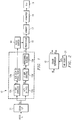
- Figure 1 is a block diagram of video-related components of a digital television receiver.
- Figure 2 illustrates a programmable version of the receiver of Figure 1.
- Figure 1 illustrates components of a digital receiver 10. It should be understood that only components used for obtaining output pixel data are shown; components used for tasks such as synchronization and audio signal processing are not shown.
- receiver 10 could be any type of equipment for receiving an analog composite video signal and displaying or storing images represented by the signal.
- Receiver 10 has a spatial light modulator (SLM) display, characterized by individually addressable pixel elements, which are capable of being turned on or off simultaneously. Images are formed by addressing those pixels that are to be turned on during an image frame, and by controlling the length of time per frame that each pixel element is on.
- SLM spatial light modulator
- the video input may be any analog signal having chrominance and luminance components.
- the luminance component is referred to herein as the "Y” component, and the chrominance component as the "C” component.
- the input signal is such that the sampling frequency for digital color separation is not the same as the sampling frequency that will provide the desired number of output pixels per line.
- the input signal is an NTSC signal, it has a 3.58 MHz color burst, which serves as a synchronizing signal to establish a frequency and phase reference for chrominance.
- the input signal is sampled at the rate appropriate for digital color separation, the result is a different number of samples per line than the desired horizontal resolution.
- a signal interface 11 provides conventional signal interface functions, such as tuning and filtering. It may also perform tasks such as synchronization signal removal, not related to the subject of the invention.
- the main function of interface 11 is to provide a composite Y/C signal to two different paths of a color separation unit 12.
- an analog Y separator 12a receives the composite input video signal.
- Separator 12a may be any analog means for separating the luminance from the chrominance components of the input signal, to produce a luminance signal. Conventional analog color separation methods, such as notch or comb filtering may be used.
- a first analog-to-digital (A/D) converter 12b receives the Y signal and samples it at a rate compatible with the desired number of output pixels per row.
- the required sampling rate is determined by the desired number of pixels per line and the horizontal scan time for active video information. For example, in the NTSC signal, the line period is 63.5 microseconds, of which approximately 52.4 microseconds represent active video information.
- the rate of sampling by A/D converter 12c is referred to herein as the "output pixel rate" because it is derived as a function of the number of pixels per line to be displayed.
- one function of field buffer 14 may be "field spreading" for SLM-based receivers, which do not require blanking periods. Field spreading permits the active video data to be “spread” throughout the field period, thereby reducing the pixel rate required for delivering data to SLM 18.
- a second A/D converter 12c receives the composite video input signal. It samples the signal at approximately 14.318 MHz, which is 4 times the 3.58 MHz subcarrier frequency. Because the color signal has 455/2 cycles per line, this 4 fsc rate results in 910 cycles per line. As a result, each row of the input signal is sampled 910 times. Of these 910 samples, approximately 750 represent active video data, with the rest being blanking information.
- a digital C separation unit 12d separates the Y data from the C data, and outputs a C signal. Conventional digital color separation methods may be used to implement C separation unit 12d.
- Y data and C data are separated and are available in digital form. However, the Y and C signals have been sampled at different rates.
- the Y data is compatible with the desired horizontal resolution, but the C data is not.
- the following table illustrates the pixel data characteristics after Y/C separation and sampling: aspect ratio 4:3 16:9 Y data 853 640 C data 750 750
- the C data is scaled by horizontal scaling unit 12e.
- the scaling converts each row of 763 pixels into a row of the proper number of output pixels.
- the 750 samples are scaled to 853 samples, each sample representing the chrominance data for one output pixel.
- the 750 samples are scaled to 640 samples.
- any one of a number of scaling algorithms may be used for scaling.
- one example of a simple scaling algorithm is bilinear interpolation, in which two adjacent samples are used to create a new sample.
- "near neighbor" methods may be used. Because the ratio 750/853 is approximately 9/10, for every 9 samples, a new sample is created.
- some scaling algorithms may result in oversampling or undersampling, such that the number of samples is not necessarily exactly the same as the desired number of output pixels.
- scaling unit 12e may be made programmable so that the scaling ratio can be varied according to the desired aspect ratio.
- scaling unit 12e is shown in Figure 1 as a stand-alone processing unit, its functions may be performed by processing unit 15, which is programmed to perform a scaling algorithm as well as to perform other processing tasks described below. Also, the horizontal scaling could be performed by processing unit 15 at various points in the chrominance processing path.
- Processing unit 15 performs various video processing algorithms, such as converting the digital signals from color difference signals to RGB, progressive scan conversion, and de-gamma correction.
- Memory 17 is an active memory for pixel data during processing by processor 15, as well as a frame memory for providing pixel data to SLM 19.
- the data is delivered in "bit-planes", formatted by formatter 18.
- U.S. Patent Serial No. (Atty Dkt No. TI-17855) incorporated by reference above, describes memory 17, formatter 18, and SLM 19 in further detail and is incorporated herein by reference.
- SLM 19 has an output format that can vary depending on the sampling rate of A/D converter 12b and the scaling factor of scaling unit 12e. Consistent with the examples of this description, SLM 19 might display 640 by 480 pixels for a 4:3 aspect ratio, or 853 by 480 pixels for a 16:9 aspect ratio.
- color separation unit 12 could be used with a digital receiver that has a CRT display. Instead of formatter 18 and SLM 19, the receiver would have a CRT (not shown). For such receivers, the data is converted back to analog form and scanned to the CRT instead of being delivered to SLM 18.
- Figure 2 illustrates a programmable version of the color separator of Figure 1.
- both A/D converter 12b and scaling unit 12e may be made programmable.
- a HR select unit 21 permits a user to select a setting for whatever format corresponds to the incoming television signal. Control signals for the appropriate sampling rate and scale factor are determined and delivered to A/D converter 12b and scaling unit 12e, respectively.
Applications Claiming Priority (2)
| Application Number | Priority Date | Filing Date | Title |
|---|---|---|---|
| US129716 | 1993-09-30 | ||
| US08/129,716 US5347321A (en) | 1993-09-30 | 1993-09-30 | Color separator for digital television |
Publications (3)
| Publication Number | Publication Date |
|---|---|
| EP0647070A2 true EP0647070A2 (de) | 1995-04-05 |
| EP0647070A3 EP0647070A3 (de) | 1995-10-11 |
| EP0647070B1 EP0647070B1 (de) | 1999-04-14 |
Family
ID=22441252
Family Applications (1)
| Application Number | Title | Priority Date | Filing Date |
|---|---|---|---|
| EP94115121A Expired - Lifetime EP0647070B1 (de) | 1993-09-30 | 1994-09-26 | Farbtrennungsgerät und Verfahren für digitales Fernsehen |
Country Status (6)
| Country | Link |
|---|---|
| US (1) | US5347321A (de) |
| EP (1) | EP0647070B1 (de) |
| JP (1) | JPH07203480A (de) |
| CN (1) | CN1082318C (de) |
| CA (1) | CA2132466A1 (de) |
| DE (1) | DE69417833T2 (de) |
Families Citing this family (39)
| Publication number | Priority date | Publication date | Assignee | Title |
|---|---|---|---|---|
| US6219015B1 (en) | 1992-04-28 | 2001-04-17 | The Board Of Directors Of The Leland Stanford, Junior University | Method and apparatus for using an array of grating light valves to produce multicolor optical images |
| US5499060A (en) * | 1994-01-04 | 1996-03-12 | Texas Instruments Incorporated | System and method for processing video data |
| US5706061A (en) * | 1995-03-31 | 1998-01-06 | Texas Instruments Incorporated | Spatial light image display system with synchronized and modulated light source |
| US5841579A (en) | 1995-06-07 | 1998-11-24 | Silicon Light Machines | Flat diffraction grating light valve |
| CA2184128A1 (en) * | 1995-08-31 | 1997-03-01 | Stephen W. Marshall | Color demodulation for digital television |
| US5990982A (en) | 1995-12-21 | 1999-11-23 | Texas Instruments Incorporated | DMD-based projector for institutional use |
| JPH09224260A (ja) * | 1996-02-19 | 1997-08-26 | Matsushita Electric Ind Co Ltd | Y/c分離装置 |
| DE19609193A1 (de) * | 1996-03-09 | 1997-09-11 | Thomson Brandt Gmbh | Verfahren und Schaltungsanordnung zum Trennen von Luminanz- und Chrominanzsignalen eines FBAS-Signals |
| US5815220A (en) * | 1996-08-30 | 1998-09-29 | Texas Instruments Incorporated | Color demodulation for digital television |
| US5982553A (en) | 1997-03-20 | 1999-11-09 | Silicon Light Machines | Display device incorporating one-dimensional grating light-valve array |
| JPH10336690A (ja) * | 1997-05-29 | 1998-12-18 | Brother Ind Ltd | 画像信号入力装置 |
| KR100222994B1 (ko) * | 1997-10-23 | 1999-10-01 | 윤종용 | 디지털 방송 수신기의 아날로그 방송 수신방법 및 장치 |
| US6088102A (en) | 1997-10-31 | 2000-07-11 | Silicon Light Machines | Display apparatus including grating light-valve array and interferometric optical system |
| US6271808B1 (en) | 1998-06-05 | 2001-08-07 | Silicon Light Machines | Stereo head mounted display using a single display device |
| US6101036A (en) | 1998-06-23 | 2000-08-08 | Silicon Light Machines | Embossed diffraction grating alone and in combination with changeable image display |
| US6130770A (en) | 1998-06-23 | 2000-10-10 | Silicon Light Machines | Electron gun activated grating light valve |
| US6215579B1 (en) | 1998-06-24 | 2001-04-10 | Silicon Light Machines | Method and apparatus for modulating an incident light beam for forming a two-dimensional image |
| US6303986B1 (en) | 1998-07-29 | 2001-10-16 | Silicon Light Machines | Method of and apparatus for sealing an hermetic lid to a semiconductor die |
| US6707591B2 (en) | 2001-04-10 | 2004-03-16 | Silicon Light Machines | Angled illumination for a single order light modulator based projection system |
| JP3476787B2 (ja) * | 2001-04-20 | 2003-12-10 | 松下電器産業株式会社 | 表示装置及び表示方法 |
| US6782205B2 (en) | 2001-06-25 | 2004-08-24 | Silicon Light Machines | Method and apparatus for dynamic equalization in wavelength division multiplexing |
| US6747781B2 (en) | 2001-06-25 | 2004-06-08 | Silicon Light Machines, Inc. | Method, apparatus, and diffuser for reducing laser speckle |
| US6829092B2 (en) | 2001-08-15 | 2004-12-07 | Silicon Light Machines, Inc. | Blazed grating light valve |
| US6800238B1 (en) | 2002-01-15 | 2004-10-05 | Silicon Light Machines, Inc. | Method for domain patterning in low coercive field ferroelectrics |
| US6767751B2 (en) | 2002-05-28 | 2004-07-27 | Silicon Light Machines, Inc. | Integrated driver process flow |
| US6728023B1 (en) | 2002-05-28 | 2004-04-27 | Silicon Light Machines | Optical device arrays with optimized image resolution |
| US6822797B1 (en) | 2002-05-31 | 2004-11-23 | Silicon Light Machines, Inc. | Light modulator structure for producing high-contrast operation using zero-order light |
| US6829258B1 (en) | 2002-06-26 | 2004-12-07 | Silicon Light Machines, Inc. | Rapidly tunable external cavity laser |
| US6813059B2 (en) | 2002-06-28 | 2004-11-02 | Silicon Light Machines, Inc. | Reduced formation of asperities in contact micro-structures |
| US6714337B1 (en) | 2002-06-28 | 2004-03-30 | Silicon Light Machines | Method and device for modulating a light beam and having an improved gamma response |
| US6801354B1 (en) | 2002-08-20 | 2004-10-05 | Silicon Light Machines, Inc. | 2-D diffraction grating for substantially eliminating polarization dependent losses |
| US6712480B1 (en) | 2002-09-27 | 2004-03-30 | Silicon Light Machines | Controlled curvature of stressed micro-structures |
| US20040155983A1 (en) * | 2003-02-10 | 2004-08-12 | Topper Robert J. | Reduced artifact luminance/chrominance (Y/C) separator for use in an NTSC decoder |
| US6829077B1 (en) | 2003-02-28 | 2004-12-07 | Silicon Light Machines, Inc. | Diffractive light modulator with dynamically rotatable diffraction plane |
| US6806997B1 (en) | 2003-02-28 | 2004-10-19 | Silicon Light Machines, Inc. | Patterned diffractive light modulator ribbon for PDL reduction |
| US20040179141A1 (en) * | 2003-03-10 | 2004-09-16 | Topper Robert J. | Method, apparatus, and system for reducing cross-color distortion in a composite video signal decoder |
| CN101547362B (zh) * | 2009-05-06 | 2010-11-24 | 天津大学 | 宽色域数字电视信号的兼容传输方法 |
| US8798171B2 (en) * | 2010-06-28 | 2014-08-05 | Richwave Technology Corp. | Video transmission by decoupling color components |
| KR102238151B1 (ko) * | 2015-03-25 | 2021-04-08 | 한화테크윈 주식회사 | 영상 신호 변환 장치 및 방법 |
Citations (3)
| Publication number | Priority date | Publication date | Assignee | Title |
|---|---|---|---|---|
| GB2154093A (en) * | 1984-02-03 | 1985-08-29 | Rca Corp | Reduced data rate signal separation system |
| US5041904A (en) * | 1988-03-31 | 1991-08-20 | Hitachi, Ltd. | Video signal processing circuit |
| US5194940A (en) * | 1991-10-03 | 1993-03-16 | Zenith Electronics Corporation | Frequency multiplexed digital video processor |
-
1993
- 1993-09-30 US US08/129,716 patent/US5347321A/en not_active Expired - Lifetime
-
1994
- 1994-09-20 CA CA002132466A patent/CA2132466A1/en not_active Abandoned
- 1994-09-26 EP EP94115121A patent/EP0647070B1/de not_active Expired - Lifetime
- 1994-09-26 DE DE69417833T patent/DE69417833T2/de not_active Expired - Fee Related
- 1994-09-30 JP JP6237787A patent/JPH07203480A/ja active Pending
- 1994-09-30 CN CN94116704.6A patent/CN1082318C/zh not_active Expired - Fee Related
Patent Citations (3)
| Publication number | Priority date | Publication date | Assignee | Title |
|---|---|---|---|---|
| GB2154093A (en) * | 1984-02-03 | 1985-08-29 | Rca Corp | Reduced data rate signal separation system |
| US5041904A (en) * | 1988-03-31 | 1991-08-20 | Hitachi, Ltd. | Video signal processing circuit |
| US5194940A (en) * | 1991-10-03 | 1993-03-16 | Zenith Electronics Corporation | Frequency multiplexed digital video processor |
Also Published As
| Publication number | Publication date |
|---|---|
| DE69417833T2 (de) | 1999-10-21 |
| US5347321A (en) | 1994-09-13 |
| EP0647070A3 (de) | 1995-10-11 |
| EP0647070B1 (de) | 1999-04-14 |
| JPH07203480A (ja) | 1995-08-04 |
| CN1082318C (zh) | 2002-04-03 |
| DE69417833D1 (de) | 1999-05-20 |
| CN1108848A (zh) | 1995-09-20 |
| CA2132466A1 (en) | 1995-03-31 |
Similar Documents
| Publication | Publication Date | Title |
|---|---|---|
| EP0647070B1 (de) | Farbtrennungsgerät und Verfahren für digitales Fernsehen | |
| US5459528A (en) | Video signal processor and method for secondary images | |
| EP0661889B1 (de) | Verfahren und Vorrichtung zur Verarbeitung von Videodaten | |
| US5796442A (en) | Multi-format television reciever | |
| US5587928A (en) | Computer teleconferencing method and apparatus | |
| EP0651577B1 (de) | Digitales Fernsehsystem | |
| CA1230669A (en) | Progressive scan television display system | |
| KR960006532B1 (ko) | 텔레비젼 신호 처리 회로 | |
| US5838385A (en) | Sampling analog video signal for secondary images | |
| WO1990013980A1 (en) | Scan converter for a high definition television system | |
| US5815220A (en) | Color demodulation for digital television | |
| KR100332329B1 (ko) | 영상신호변환장치 | |
| EP0710016A2 (de) | Fernsehempfänger für Rundfunksignale mit verschiedenen Anzeigeformaten | |
| US4518984A (en) | Device for flicker-free reproduction of television pictures and text and graphics pages | |
| US5587744A (en) | Image display apparatus | |
| EP0862334A2 (de) | Signalverarbeitungssystem | |
| EP0762752A2 (de) | Abtasten eines analogen Videosignals für sekundäre Bilder | |
| KR100480569B1 (ko) | 다기능 비디오 디코더 | |
| KR920003720B1 (ko) | 디지탈 신호 처리 장치 | |
| EP0454116A2 (de) | Fernsehsignalumwandler | |
| EP0762782B1 (de) | Farbdemodulation für digitales Fernsehen | |
| JPH09102935A (ja) | 特別な特徴を具備した低価格順次走査型テレビジョンシステム | |
| JPS63316583A (ja) | 2チャネル広アスペクト比テレビジョン信号伝送システムの1チェネル上で拡大パネル成分を伝送する方法と装置 | |
| JPH0213076A (ja) | テレビジョン信号受信装置 | |
| JPH0394595A (ja) | 映像信号変換装置 |
Legal Events
| Date | Code | Title | Description |
|---|---|---|---|
| PUAI | Public reference made under article 153(3) epc to a published international application that has entered the european phase |
Free format text: ORIGINAL CODE: 0009012 |
|
| AK | Designated contracting states |
Kind code of ref document: A2 Designated state(s): DE FR GB IT NL |
|
| PUAL | Search report despatched |
Free format text: ORIGINAL CODE: 0009013 |
|
| AK | Designated contracting states |
Kind code of ref document: A3 Designated state(s): DE FR GB IT NL |
|
| 17P | Request for examination filed |
Effective date: 19960325 |
|
| GRAG | Despatch of communication of intention to grant |
Free format text: ORIGINAL CODE: EPIDOS AGRA |
|
| 17Q | First examination report despatched |
Effective date: 19980529 |
|
| GRAG | Despatch of communication of intention to grant |
Free format text: ORIGINAL CODE: EPIDOS AGRA |
|
| GRAG | Despatch of communication of intention to grant |
Free format text: ORIGINAL CODE: EPIDOS AGRA |
|
| GRAH | Despatch of communication of intention to grant a patent |
Free format text: ORIGINAL CODE: EPIDOS IGRA |
|
| GRAH | Despatch of communication of intention to grant a patent |
Free format text: ORIGINAL CODE: EPIDOS IGRA |
|
| GRAA | (expected) grant |
Free format text: ORIGINAL CODE: 0009210 |
|
| ITF | It: translation for a ep patent filed |
Owner name: BARZANO' E ZANARDO ROMA S.P.A. |
|
| AK | Designated contracting states |
Kind code of ref document: B1 Designated state(s): DE FR GB IT NL |
|
| REF | Corresponds to: |
Ref document number: 69417833 Country of ref document: DE Date of ref document: 19990520 |
|
| ET | Fr: translation filed | ||
| PLBE | No opposition filed within time limit |
Free format text: ORIGINAL CODE: 0009261 |
|
| STAA | Information on the status of an ep patent application or granted ep patent |
Free format text: STATUS: NO OPPOSITION FILED WITHIN TIME LIMIT |
|
| 26N | No opposition filed | ||
| REG | Reference to a national code |
Ref country code: GB Ref legal event code: IF02 |
|
| PGFP | Annual fee paid to national office [announced via postgrant information from national office to epo] |
Ref country code: IT Payment date: 20060930 Year of fee payment: 13 |
|
| PGFP | Annual fee paid to national office [announced via postgrant information from national office to epo] |
Ref country code: NL Payment date: 20080813 Year of fee payment: 15 Ref country code: FR Payment date: 20080904 Year of fee payment: 15 |
|
| PGFP | Annual fee paid to national office [announced via postgrant information from national office to epo] |
Ref country code: GB Payment date: 20080808 Year of fee payment: 15 |
|
| PGFP | Annual fee paid to national office [announced via postgrant information from national office to epo] |
Ref country code: DE Payment date: 20080930 Year of fee payment: 15 |
|
| PG25 | Lapsed in a contracting state [announced via postgrant information from national office to epo] |
Ref country code: IT Free format text: LAPSE BECAUSE OF NON-PAYMENT OF DUE FEES Effective date: 20070926 |
|
| REG | Reference to a national code |
Ref country code: NL Ref legal event code: V1 Effective date: 20100401 |
|
| GBPC | Gb: european patent ceased through non-payment of renewal fee |
Effective date: 20090926 |
|
| REG | Reference to a national code |
Ref country code: FR Ref legal event code: ST Effective date: 20100531 |
|
| PG25 | Lapsed in a contracting state [announced via postgrant information from national office to epo] |
Ref country code: NL Free format text: LAPSE BECAUSE OF NON-PAYMENT OF DUE FEES Effective date: 20100401 Ref country code: FR Free format text: LAPSE BECAUSE OF NON-PAYMENT OF DUE FEES Effective date: 20090930 Ref country code: DE Free format text: LAPSE BECAUSE OF NON-PAYMENT OF DUE FEES Effective date: 20100401 |
|
| PG25 | Lapsed in a contracting state [announced via postgrant information from national office to epo] |
Ref country code: GB Free format text: LAPSE BECAUSE OF NON-PAYMENT OF DUE FEES Effective date: 20090926 |