EP0646972B1 - Improvements in or relating to detector arrays - Google Patents
Improvements in or relating to detector arrays Download PDFInfo
- Publication number
- EP0646972B1 EP0646972B1 EP94307238A EP94307238A EP0646972B1 EP 0646972 B1 EP0646972 B1 EP 0646972B1 EP 94307238 A EP94307238 A EP 94307238A EP 94307238 A EP94307238 A EP 94307238A EP 0646972 B1 EP0646972 B1 EP 0646972B1
- Authority
- EP
- European Patent Office
- Prior art keywords
- aperture
- radiation
- baffle
- detector
- detector array
- Prior art date
- Legal status (The legal status is an assumption and is not a legal conclusion. Google has not performed a legal analysis and makes no representation as to the accuracy of the status listed.)
- Expired - Lifetime
Links
- 238000003491 array Methods 0.000 title description 2
- 230000005855 radiation Effects 0.000 claims description 48
- 239000000463 material Substances 0.000 claims description 7
- 230000005540 biological transmission Effects 0.000 claims description 5
- 238000000576 coating method Methods 0.000 description 24
- 230000003595 spectral effect Effects 0.000 description 14
- 230000003287 optical effect Effects 0.000 description 11
- 239000011248 coating agent Substances 0.000 description 8
- 229910052751 metal Inorganic materials 0.000 description 7
- 239000002184 metal Substances 0.000 description 7
- 229910052782 aluminium Inorganic materials 0.000 description 4
- XAGFODPZIPBFFR-UHFFFAOYSA-N aluminium Chemical compound [Al] XAGFODPZIPBFFR-UHFFFAOYSA-N 0.000 description 4
- 238000001816 cooling Methods 0.000 description 4
- 239000010408 film Substances 0.000 description 3
- 230000004907 flux Effects 0.000 description 3
- 239000003973 paint Substances 0.000 description 3
- 239000000758 substrate Substances 0.000 description 3
- 239000011358 absorbing material Substances 0.000 description 2
- 239000006229 carbon black Substances 0.000 description 2
- 238000010276 construction Methods 0.000 description 2
- 230000008021 deposition Effects 0.000 description 2
- 238000010586 diagram Methods 0.000 description 2
- 238000003384 imaging method Methods 0.000 description 2
- 230000007246 mechanism Effects 0.000 description 2
- 230000004044 response Effects 0.000 description 2
- PFNQVRZLDWYSCW-UHFFFAOYSA-N (fluoren-9-ylideneamino) n-naphthalen-1-ylcarbamate Chemical compound C12=CC=CC=C2C2=CC=CC=C2C1=NOC(=O)NC1=CC=CC2=CC=CC=C12 PFNQVRZLDWYSCW-UHFFFAOYSA-N 0.000 description 1
- VYZAMTAEIAYCRO-UHFFFAOYSA-N Chromium Chemical compound [Cr] VYZAMTAEIAYCRO-UHFFFAOYSA-N 0.000 description 1
- 239000004593 Epoxy Substances 0.000 description 1
- 239000000853 adhesive Substances 0.000 description 1
- 239000004411 aluminium Substances 0.000 description 1
- 238000013459 approach Methods 0.000 description 1
- 239000012298 atmosphere Substances 0.000 description 1
- 229910052804 chromium Inorganic materials 0.000 description 1
- 239000011651 chromium Substances 0.000 description 1
- 239000003086 colorant Substances 0.000 description 1
- 230000003247 decreasing effect Effects 0.000 description 1
- 238000001514 detection method Methods 0.000 description 1
- 238000009501 film coating Methods 0.000 description 1
- 229910052732 germanium Inorganic materials 0.000 description 1
- GNPVGFCGXDBREM-UHFFFAOYSA-N germanium atom Chemical compound [Ge] GNPVGFCGXDBREM-UHFFFAOYSA-N 0.000 description 1
- PCHJSUWPFVWCPO-UHFFFAOYSA-N gold Chemical compound [Au] PCHJSUWPFVWCPO-UHFFFAOYSA-N 0.000 description 1
- 239000010931 gold Substances 0.000 description 1
- 229910052737 gold Inorganic materials 0.000 description 1
- 238000002955 isolation Methods 0.000 description 1
- 238000000034 method Methods 0.000 description 1
- 230000008569 process Effects 0.000 description 1
- 238000002310 reflectometry Methods 0.000 description 1
- 230000035945 sensitivity Effects 0.000 description 1
- 230000001629 suppression Effects 0.000 description 1
- 239000010409 thin film Substances 0.000 description 1
Images

Classifications
-
- G—PHYSICS
- G01—MEASURING; TESTING
- G01J—MEASUREMENT OF INTENSITY, VELOCITY, SPECTRAL CONTENT, POLARISATION, PHASE OR PULSE CHARACTERISTICS OF INFRARED, VISIBLE OR ULTRAVIOLET LIGHT; COLORIMETRY; RADIATION PYROMETRY
- G01J5/00—Radiation pyrometry, e.g. infrared or optical thermometry
-
- H—ELECTRICITY
- H01—ELECTRIC ELEMENTS
- H01L—SEMICONDUCTOR DEVICES NOT COVERED BY CLASS H10
- H01L31/00—Semiconductor devices sensitive to infrared radiation, light, electromagnetic radiation of shorter wavelength or corpuscular radiation and specially adapted either for the conversion of the energy of such radiation into electrical energy or for the control of electrical energy by such radiation; Processes or apparatus specially adapted for the manufacture or treatment thereof or of parts thereof; Details thereof
- H01L31/02—Details
- H01L31/0216—Coatings
- H01L31/02161—Coatings for devices characterised by at least one potential jump barrier or surface barrier
- H01L31/02162—Coatings for devices characterised by at least one potential jump barrier or surface barrier for filtering or shielding light, e.g. multicolour filters for photodetectors
- H01L31/02164—Coatings for devices characterised by at least one potential jump barrier or surface barrier for filtering or shielding light, e.g. multicolour filters for photodetectors for shielding light, e.g. light blocking layers, cold shields for infrared detectors
-
- G—PHYSICS
- G01—MEASURING; TESTING
- G01J—MEASUREMENT OF INTENSITY, VELOCITY, SPECTRAL CONTENT, POLARISATION, PHASE OR PULSE CHARACTERISTICS OF INFRARED, VISIBLE OR ULTRAVIOLET LIGHT; COLORIMETRY; RADIATION PYROMETRY
- G01J5/00—Radiation pyrometry, e.g. infrared or optical thermometry
- G01J5/02—Constructional details
- G01J5/06—Arrangements for eliminating effects of disturbing radiation; Arrangements for compensating changes in sensitivity
Definitions
- This invention relates to a cold shield and cold filter for infrared detector arrays.
- the sensitivity of infrared detectors depends upon both their signal response and upon the noise associated with the detection process.
- the most sensitive such detectors are photon detectors, that is, those detectors whose signal response is proportional to the number of photons incident thereon.
- the limit of performance of such detectors is set by the random fluctuations in the rate at which background photons are received. Detectors for which this is true are generally referred to as "background limited”.
- the magnitude of the fluctuation energy is very nearly proportional to the total number of photons detected. It follows that, for photon detectors, the output signal-to-noise ratio is maximized by rejecting all radiation that does not contribute appreciably to the signal while accepting all radiation that does so contribute.
- Radiation which contributes to the signal at the detector plane is defined in two ways: (1) geometrically and (2) spectrally.
- the geometric definition is determined by the optical system associated with the detector array. All energy gathering and imaging optical systems have an aperture and an aperture stop which determines how much energy is gathered by a detector element.
- the spectral definition is determined by the type of radiation source being detected, modified by the spectral transmission of the atmosphere intervening between the source and the optics and detector. Maximizing the signal requires that the vacuum chamber, generally a Dewar, be so constructed that as much of the geometric and spectral content of the signal as possible be accepted.
- both maximizing the signal collected and minimizing the non-signal radiation collected can be accomplished by making the aperture stop a physical part of the detector. Any surfaces that are within the view of the detector array outside the aperture stop must be cold and black (highly emissive and low reflecting) so that they produce a negligible photon flux at the detector array. These surfaces are usually cooled by the same cooling mechanism employed to cool the detector array. All known "background limited" photon detectors must be cooled to reduce other detector noise mechanisms to a level below that induced by the background flux.
- the photon detectors are mounted in thermal contact with the cooling means, are packaged within a vacuum space for thermal isolation and receive the signal radiation through an optical window placed in one wall of the vacuum space.
- the problem being addressed is that of configuring a detector array within a vacuum space, with an aperture or stop defining the geometrical limits and a spectral filter defining the spectral limits of the radiation the detector array can receive.
- FIGURES 1a to 1d illustrate several prior art approaches to solving the problem as set forth above.
- the configuration of FIGURE 1a includes a vacuum containing vessel having a vacuum wall 3, which can be a Dewar, having a detector array 4 therein.
- the side of the enclosure facing the detector array 4 includes a wall 7 of a material opaque to incoming radiation and which is secured to the vacuum wall 3.
- the wall 7 has an aperture 1 therein and a window 2 having a filter coating or coatings 5 thereon secured to the wall 7 and disposed over the aperture to provide the aperture with a filter thereover for incoming radiations to the detector array 4.
- This configuration places spectral filter coatings on one or both surfaces of the vacuum window 2 and places the aperture 1 on the interior surface of the window.
- the detector can receive radiation both emitted by the warm vacuum wall as well as reflected by the wall from other surfaces within the vacuum. This is a poor solution to the problem because a significant amount of radiation can reach the detector which originates external to the geometrical limits of the aperture 1 and external to the spectral limits of the filter coatings 5.
- FIGURE 1b The configuration of FIGURE 1b is the same as in FIGURE 1a except that the filter coating 5 is disposed within the vacuum vessel and between the detector array 4 and the aperture 1.
- This configuration achieves a somewhat better result than that of FIGURE 1a by placment of the filter coatings on a substrate immediately in front of the detector array.
- the coatings on the window can now become anti-reflectance coatings which provide high transmission over the filter spectral band.
- the spectral content of the radiation impinging on the detector array is now restricted to the desired pass band.
- the detector is still not restricted geometrically, however, so it can still receive spurious radiation by way of the vacuum wall.
- This configuration has the additional drawback that the filter substrate 8 adds mass to the cooled region, thereby adding to the time required to cool the detector array 4 to its operating temperature.
- FIGURE 1c is an improved version of FIGURE 1a except that the wall 7 is removed and the window 2 with filter coating 5 thereon is secured to the vacuum wall 3 directly to provide the vacuum vessel.
- a baffle 6 is provided within the vacuum vessel and has an aperture 1 therein through which radiation travels to the detector array 4 at the surface of the baffle opposing the aperture. This configuration moves the aperture 1 to an enclosed shield or baffle 6 surrounding the detector array 4. Coating the interior surface of this baffle 6 with a highly emissive (therefore low reflecting) coating reduces the radiation reaching the detector array 4 from the baffle interior to a negligible amount.
- the aperture 1 of this baffle now becomes the aperture stop of the optical system, establishing a limit to the angles at which the detector array 4 can receive radiation.
- the top, outer surface of the baffle 6 is highly emissive, this configuration achieves the desired geometric and spectral restriction of background radiation. If the surface is reflective, however, a significant amount of spurious radiation can reach the detector array 4 by multiple reflections between the window surfaces 2 and the top surface of the baffle. Since this radiation is not filtered by the window coatings, it will be at wavelengths outside the spectral bandpass of the window.
- FIGURE 1c The major drawback of the configuration of FIGURE 1c is the inaccessibility of the aperture 1. Since either the window substrate 2 or its coatings 5 are usually visibly opaque, the location of the aperture 1 cannot be determined by visible means. Another drawback is the necessity to strike a compromise between baffle rigidity and heat load imposed upon the cooling means. The baffle 6 must have sufficient mass to make it rigid enough to avoid motion of the aperture 1 with respect to the optical system, thereby modulating the background radiation reaching the detector array 4 and creating a spurious signal. Too much mass increases the time required to cool the baffle 6 and detector array 4 to operating temperature.
- FIGURE 1d is a combination of the configurations of FIGURES 1b and 1c and uses the filter position of FIGURE 1b and the aperture position of FIGURE 1c.
- the drawbacks to this configuration are aperture inaccessiblity, lack of rigidity and excess cool-down time.
- EP-A-0 490 166 proposes a detector assembly in which the front wall of the vacuum-containing vessel is opaque, with a window set into it, and there is an inner baffle with an aperture aligned with the window.
- US-A 4 996 427 proposes a similar detector assembly with the window on the outside of the front wall.
- Band pass filters for different frequency bands covering the two halves of the detector array, and a similar pair of filters cover the two halves of a fresnel biprism in front of the imaging optics outside the vacuum vessel, so that the two halves of the detector array can view the same object in different colours.
- the present invention solves the problem of eliminating spurious radiation in a particularly attractive way with all of the advantages and few of the disadvantages of the prior art solutions as demonstrated hereinabove.
- Typical broad spectrum absorptive coatings that can be used are paints with a high carbon black content or evaporated multi-layer coatings with a highly absorbing semi-metal as one of the layers.
- Typical reflective coatings that can be used are evaporated or sputtered metal films of aluminium, gold, or chromium.
- the invention provides a cold shield which comprises: an evacuated enclosure defined by walls one of which has a first aperture for transmission of radiations; and a baffle disposed within said enclosure, spaced from the walls of the enclosure and having a second aperture aligned with said first aperture and having a detector disposed on a surface thereof opposite said second aperture; characterised in that: the said one wall includes a radiation transmissive member and a radiation opaque member; the radiation transmissive member has a radiation band pass filter disposed thereon; and the radiation opaque member defines the first aperture and is disposed on the surface of the radiation transmissive member external to the evacuated enclosure.
- the invention concerns also a detector array including such a cold shield.
- the aperture stop of the optical system is placed on the outer surface of and external to the vacuum window, it is easily accessible for alignment purposes as compared with the above described prior art.
- the preferred means for defining the aperture stop is by deposition of highly reflecting, opaque film.
- a machined aperture in a highly reflective metal plate or deposited metal with aperture, placed in proximity to the window, can also be used.
- a baffle is placed within the vacuum space, surrounding the detector array, with an aperture that is just larger than the aperture stop on the window so that the total radiation reaching the detector is restricted, but the signal radiation as defined by the aperture stop is not so restricted.
- the baffle need not be of heavy construction since it can be permitted to move slightly under vibration so long as it does not encroach into the space occupied by the signal radiation.
- the baffle can therefore be light weight relative to the above described prior art baffles and preferably is of a material having low specific heat, preferably aluminum. Thereby, the baffle requires less cooling power than the rigid higher mass prior art baffles and cools down more quickly.
- the vacuum window is constructed of a non-radiation-absorbing material and coated to serve as a bandpass filter. Both the interior surface of the baffle and its top outer surface are coated to be highly absorptive. Typical highly absorptive coatings that can be used are paints with a high carbon black content or evaporated multi-layer coatings with a highly absorbing semi-metal as one of the layers.
- the present invention provides about the same signal-to-noise ratio as the better prior art configurations and provides a better signal-to-noise ratio than the other prior art configurations.
- the present invention essentially matches the signal-to-noise ratio of the better prior art configurations by providing a slightly higher signal level, offsetting a slightly higher noise level.
- the signal level of the present invention equals or exceeds that of the other configurations because it uses only one rather than two optical elements. Since the filter transmissions of all configurations are the same, the lack of a second optical element in the present invention provides a greater signal level.
- the noise level of the present invention is slightly higher than the better prior art configurations because of the emission of the small area around the perimeter of the aperture stop which is exposed to the detector. The emitted radiation is minimized by making the aperture material have a high reflectivity and therefore a low emissivity.
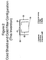
- FIGURE 2 there is shown a cold shield and cold filter in accordance with the present invention.
- the configuration of FIGURE 2 includes a vacuum containing vessel having a vacuum wall 3, which can be a Dewar, and a window 2 with filter coating 5 thereon which is secured directly to the vacuum wall to provide the vacuum vessel.
- the aperture stop 1 of the optical system is preferably a light reflecting material with the aperture therein, for example, an evaporated aluminum coating or a piece of metal with an aperture cut therein which is secured to the outer surface of the vacuum window 2 by an epoxy or other adhesive agent.
- the preferred means for defining the aperture stop is by deposition of a highly reflecting, opaque film, preferably aluminum. A machined aperture in a highly reflective metal plate, placed in proximity to the window can also be used.
- a baffle 6 is placed within the vacuum space, surrounding the detector array 4 with an aperture that is just larger than the aperture stop 1 on the window 2 so that it restricts the total radiation reaching the detector array, but not the signal radiation as defined by the aperture stop.
- the baffle need not be of heavy construction, since it can be allowed to move slightly under vibration as long as it does not encroach into the space occupied by the signal radiation.
- the vacuum window 2 is constructed of a non-radiation-absorbing material, such as, for example, germanium, zinc selenide or other well known optical material and is coated with a suitable multi-layer evaporated thin film coating 5 to serve as an optical bandpass filter.
- Both the interior surface of the baffle 6 and its top outer surface are coated with absorptive paint or other coating absorptive to be highly emissive and therefore low reflecting to reduce the radiation reaching the detector from the baffle interior to a negligible amount. If the top, outer surface of the baffle 6 is highly emissive, this configuration achieves the desired geometric and spectral restriction of background radiation.
Landscapes
- Physics & Mathematics (AREA)
- General Physics & Mathematics (AREA)
- Spectroscopy & Molecular Physics (AREA)
- Condensed Matter Physics & Semiconductors (AREA)
- Electromagnetism (AREA)
- Engineering & Computer Science (AREA)
- Computer Hardware Design (AREA)
- Microelectronics & Electronic Packaging (AREA)
- Power Engineering (AREA)
- Radiation Pyrometers (AREA)
- Photometry And Measurement Of Optical Pulse Characteristics (AREA)
- Measurement Of Radiation (AREA)
Description
- This invention relates to a cold shield and cold filter for infrared detector arrays.
- The sensitivity of infrared detectors depends upon both their signal response and upon the noise associated with the detection process. The most sensitive such detectors are photon detectors, that is, those detectors whose signal response is proportional to the number of photons incident thereon. The limit of performance of such detectors is set by the random fluctuations in the rate at which background photons are received. Detectors for which this is true are generally referred to as "background limited". The magnitude of the fluctuation energy is very nearly proportional to the total number of photons detected. It follows that, for photon detectors, the output signal-to-noise ratio is maximized by rejecting all radiation that does not contribute appreciably to the signal while accepting all radiation that does so contribute.
- Radiation which contributes to the signal at the detector plane is defined in two ways: (1) geometrically and (2) spectrally. The geometric definition is determined by the optical system associated with the detector array. All energy gathering and imaging optical systems have an aperture and an aperture stop which determines how much energy is gathered by a detector element. The spectral definition is determined by the type of radiation source being detected, modified by the spectral transmission of the atmosphere intervening between the source and the optics and detector. Maximizing the signal requires that the vacuum chamber, generally a Dewar, be so constructed that as much of the geometric and spectral content of the signal as possible be accepted.
- Maximizing the signal-to-noise ratio requires a balance between the amount of signal collected and the amount of noise generated by the total photon flux. Geometrically, both maximizing the signal collected and minimizing the non-signal radiation collected can be accomplished by making the aperture stop a physical part of the detector. Any surfaces that are within the view of the detector array outside the aperture stop must be cold and black (highly emissive and low reflecting) so that they produce a negligible photon flux at the detector array. These surfaces are usually cooled by the same cooling mechanism employed to cool the detector array. All known "background limited" photon detectors must be cooled to reduce other detector noise mechanisms to a level below that induced by the background flux. The photon detectors are mounted in thermal contact with the cooling means, are packaged within a vacuum space for thermal isolation and receive the signal radiation through an optical window placed in one wall of the vacuum space.
- To eliminate radiation that contributes less to signal than to background because of the wavelength span it covers requires the use of a bandpass spectral filter. This filter must be placed so that no radiation having significant energy content at wavelengths outside the filter bandpass can reach the detector array.
- The problem being addressed is that of configuring a detector array within a vacuum space, with an aperture or stop defining the geometrical limits and a spectral filter defining the spectral limits of the radiation the detector array can receive.
- FIGURES 1a to 1d illustrate several prior art approaches to solving the problem as set forth above. The configuration of FIGURE 1a includes a vacuum containing vessel having a
vacuum wall 3, which can be a Dewar, having adetector array 4 therein. The side of the enclosure facing thedetector array 4 includes a wall 7 of a material opaque to incoming radiation and which is secured to thevacuum wall 3. The wall 7 has anaperture 1 therein and awindow 2 having a filter coating orcoatings 5 thereon secured to the wall 7 and disposed over the aperture to provide the aperture with a filter thereover for incoming radiations to thedetector array 4. This configuration places spectral filter coatings on one or both surfaces of thevacuum window 2 and places theaperture 1 on the interior surface of the window. The detector can receive radiation both emitted by the warm vacuum wall as well as reflected by the wall from other surfaces within the vacuum. This is a poor solution to the problem because a significant amount of radiation can reach the detector which originates external to the geometrical limits of theaperture 1 and external to the spectral limits of thefilter coatings 5. - The configuration of FIGURE 1b is the same as in FIGURE 1a except that the
filter coating 5 is disposed within the vacuum vessel and between thedetector array 4 and theaperture 1. This configuration achieves a somewhat better result than that of FIGURE 1a by placment of the filter coatings on a substrate immediately in front of the detector array. The coatings on the window can now become anti-reflectance coatings which provide high transmission over the filter spectral band. The spectral content of the radiation impinging on the detector array is now restricted to the desired pass band. The detector is still not restricted geometrically, however, so it can still receive spurious radiation by way of the vacuum wall. This configuration has the additional drawback that the filter substrate 8 adds mass to the cooled region, thereby adding to the time required to cool thedetector array 4 to its operating temperature. - The configuration of FIGURE 1c is an improved version of FIGURE 1a except that the wall 7 is removed and the
window 2 withfilter coating 5 thereon is secured to thevacuum wall 3 directly to provide the vacuum vessel. Additionally, abaffle 6 is provided within the vacuum vessel and has anaperture 1 therein through which radiation travels to thedetector array 4 at the surface of the baffle opposing the aperture. This configuration moves theaperture 1 to an enclosed shield orbaffle 6 surrounding thedetector array 4. Coating the interior surface of thisbaffle 6 with a highly emissive (therefore low reflecting) coating reduces the radiation reaching thedetector array 4 from the baffle interior to a negligible amount. Theaperture 1 of this baffle now becomes the aperture stop of the optical system, establishing a limit to the angles at which thedetector array 4 can receive radiation. If the top, outer surface of thebaffle 6 is highly emissive, this configuration achieves the desired geometric and spectral restriction of background radiation. If the surface is reflective, however, a significant amount of spurious radiation can reach thedetector array 4 by multiple reflections between thewindow surfaces 2 and the top surface of the baffle. Since this radiation is not filtered by the window coatings, it will be at wavelengths outside the spectral bandpass of the window. - The major drawback of the configuration of FIGURE 1c is the inaccessibility of the
aperture 1. Since either thewindow substrate 2 or itscoatings 5 are usually visibly opaque, the location of theaperture 1 cannot be determined by visible means. Another drawback is the necessity to strike a compromise between baffle rigidity and heat load imposed upon the cooling means. Thebaffle 6 must have sufficient mass to make it rigid enough to avoid motion of theaperture 1 with respect to the optical system, thereby modulating the background radiation reaching thedetector array 4 and creating a spurious signal. Too much mass increases the time required to cool thebaffle 6 anddetector array 4 to operating temperature. - The configuration of FIGURE 1d is a combination of the configurations of FIGURES 1b and 1c and uses the filter position of FIGURE 1b and the aperture position of FIGURE 1c. The drawbacks to this configuration are aperture inaccessiblity, lack of rigidity and excess cool-down time.
- EP-A-0 490 166, on which the preamble of
claim 1 is based, proposes a detector assembly in which the front wall of the vacuum-containing vessel is opaque, with a window set into it, and there is an inner baffle with an aperture aligned with the window. US-A 4 996 427 proposes a similar detector assembly with the window on the outside of the front wall. Band pass filters for different frequency bands covering the two halves of the detector array, and a similar pair of filters cover the two halves of a fresnel biprism in front of the imaging optics outside the vacuum vessel, so that the two halves of the detector array can view the same object in different colours. - The present invention solves the problem of eliminating spurious radiation in a particularly attractive way with all of the advantages and few of the disadvantages of the prior art solutions as demonstrated hereinabove.
- Briefly, this is accomplished by the novel placement of a baffle and an aperture, and preferably also by the use of broad spectrum absorptive and reflective coatings and by the novel placement of these coatings in combination with spectral bandpass coatings. Typical broad spectrum absorptive coatings that can be used are paints with a high carbon black content or evaporated multi-layer coatings with a highly absorbing semi-metal as one of the layers. Typical reflective coatings that can be used are evaporated or sputtered metal films of aluminium, gold, or chromium.
- The invention provides a cold shield which comprises: an evacuated enclosure defined by walls one of which has a first aperture for transmission of radiations; and a baffle disposed within said enclosure, spaced from the walls of the enclosure and having a second aperture aligned with said first aperture and having a detector disposed on a surface thereof opposite said second aperture; characterised in that: the said one wall includes a radiation transmissive member and a radiation opaque member; the radiation transmissive member has a radiation band pass filter disposed thereon; and the radiation opaque member defines the first aperture and is disposed on the surface of the radiation transmissive member external to the evacuated enclosure.
- The invention concerns also a detector array including such a cold shield.
- Because the aperture stop of the optical system is placed on the outer surface of and external to the vacuum window, it is easily accessible for alignment purposes as compared with the above described prior art. The preferred means for defining the aperture stop is by deposition of highly reflecting, opaque film. A machined aperture in a highly reflective metal plate or deposited metal with aperture, placed in proximity to the window, can also be used. A baffle is placed within the vacuum space, surrounding the detector array, with an aperture that is just larger than the aperture stop on the window so that the total radiation reaching the detector is restricted, but the signal radiation as defined by the aperture stop is not so restricted. The baffle need not be of heavy construction since it can be permitted to move slightly under vibration so long as it does not encroach into the space occupied by the signal radiation. The baffle can therefore be light weight relative to the above described prior art baffles and preferably is of a material having low specific heat, preferably aluminum. Thereby, the baffle requires less cooling power than the rigid higher mass prior art baffles and cools down more quickly. The vacuum window is constructed of a non-radiation-absorbing material and coated to serve as a bandpass filter. Both the interior surface of the baffle and its top outer surface are coated to be highly absorptive. Typical highly absorptive coatings that can be used are paints with a high carbon black content or evaporated multi-layer coatings with a highly absorbing semi-metal as one of the layers.
- The advantages of the invention over the prior art are at least threefold, these being suppression of spurious radiation without decreasing signal radiation, provision of a readily accessible aperture stop which may be rigidly supported and addition of less mass to the cooled region that in the prior art.
- The present invention provides about the same signal-to-noise ratio as the better prior art configurations and provides a better signal-to-noise ratio than the other prior art configurations. The present invention essentially matches the signal-to-noise ratio of the better prior art configurations by providing a slightly higher signal level, offsetting a slightly higher noise level.
- The signal level of the present invention equals or exceeds that of the other configurations because it uses only one rather than two optical elements. Since the filter transmissions of all configurations are the same, the lack of a second optical element in the present invention provides a greater signal level. The noise level of the present invention is slightly higher than the better prior art configurations because of the emission of the small area around the perimeter of the aperture stop which is exposed to the detector. The emitted radiation is minimized by making the aperture material have a high reflectivity and therefore a low emissivity.
-
- FIGURES 1a to 1d are schematic diagrams of prior art cold shield and cold filter configurations; and
- FIGURE 2 is a schematic diagram of a cold shield and cold filter configuration in accordance with the present invention.
-
- Referring now to FIGURE 2, there is shown a cold shield and cold filter in accordance with the present invention. The configuration of FIGURE 2 includes a vacuum containing vessel having a
vacuum wall 3, which can be a Dewar, and awindow 2 withfilter coating 5 thereon which is secured directly to the vacuum wall to provide the vacuum vessel. Theaperture stop 1 of the optical system is preferably a light reflecting material with the aperture therein, for example, an evaporated aluminum coating or a piece of metal with an aperture cut therein which is secured to the outer surface of thevacuum window 2 by an epoxy or other adhesive agent. The preferred means for defining the aperture stop is by deposition of a highly reflecting, opaque film, preferably aluminum. A machined aperture in a highly reflective metal plate, placed in proximity to the window can also be used. Abaffle 6 is placed within the vacuum space, surrounding thedetector array 4 with an aperture that is just larger than theaperture stop 1 on thewindow 2 so that it restricts the total radiation reaching the detector array, but not the signal radiation as defined by the aperture stop. The baffle need not be of heavy construction, since it can be allowed to move slightly under vibration as long as it does not encroach into the space occupied by the signal radiation. Thevacuum window 2 is constructed of a non-radiation-absorbing material, such as, for example, germanium, zinc selenide or other well known optical material and is coated with a suitable multi-layer evaporatedthin film coating 5 to serve as an optical bandpass filter. Both the interior surface of thebaffle 6 and its top outer surface are coated with absorptive paint or other coating absorptive to be highly emissive and therefore low reflecting to reduce the radiation reaching the detector from the baffle interior to a negligible amount. If the top, outer surface of thebaffle 6 is highly emissive, this configuration achieves the desired geometric and spectral restriction of background radiation.
Claims (6)
- A cold shield which comprises: an evacuated enclosure (3) defined by walls one of which has a first aperture (1) for transmission of radiations; and a baffle (6) disposed within said enclosure, spaced from the walls of the enclosure (3) and having a second aperture aligned with said first aperture (1) and having a detector (4) disposed on a surface thereof opposite said second aperture; characterised in that: the said one wall includes a radiation transmissive member and a radiation opaque member; the radiation transmissive member has a radiation band pass filter (5) disposed thereon; and the radiation opaque member defines the first aperture (1) and is disposed on the surface of the radiation transmissive member (2) external to the evacuated enclosure (3).
- The shield of claim 1, wherein said first aperture (1) is smaller than said second aperture.
- The shield of claim 1 or claim 2, wherein the interior of said baffle is coated with an absorptive, low reflecting material.
- The shield of any preceding claim, wherein the exterior surface of said baffle opposing said first aperture is coated with an absorptive, low reflecting material.
- A detector array including a cold shield according to any preceding claim.
- A detector array according to claim 5, wherein the detector is an infrared detector.
Applications Claiming Priority (2)
| Application Number | Priority Date | Filing Date | Title |
|---|---|---|---|
| US130204 | 1993-10-01 | ||
| US08/130,204 US5434413A (en) | 1993-10-01 | 1993-10-01 | Virtual cold shield and cold filter for infrared detector arrays |
Publications (3)
| Publication Number | Publication Date |
|---|---|
| EP0646972A2 EP0646972A2 (en) | 1995-04-05 |
| EP0646972A3 EP0646972A3 (en) | 1995-04-19 |
| EP0646972B1 true EP0646972B1 (en) | 2000-02-02 |
Family
ID=22443554
Family Applications (1)
| Application Number | Title | Priority Date | Filing Date |
|---|---|---|---|
| EP94307238A Expired - Lifetime EP0646972B1 (en) | 1993-10-01 | 1994-10-03 | Improvements in or relating to detector arrays |
Country Status (5)
| Country | Link |
|---|---|
| US (1) | US5434413A (en) |
| EP (1) | EP0646972B1 (en) |
| JP (1) | JPH07253358A (en) |
| KR (1) | KR100352105B1 (en) |
| DE (1) | DE69422874T2 (en) |
Families Citing this family (17)
| Publication number | Priority date | Publication date | Assignee | Title |
|---|---|---|---|---|
| US6371925B1 (en) | 1997-07-28 | 2002-04-16 | Matsushita Electric Industrial Co., Ltd. | Radiation clinical thermometer |
| US7692148B2 (en) | 2005-01-26 | 2010-04-06 | Analog Devices, Inc. | Thermal sensor with thermal barrier |
| US7718967B2 (en) | 2005-01-26 | 2010-05-18 | Analog Devices, Inc. | Die temperature sensors |
| US7807972B2 (en) * | 2005-01-26 | 2010-10-05 | Analog Devices, Inc. | Radiation sensor with cap and optical elements |
| US8487260B2 (en) | 2005-01-26 | 2013-07-16 | Analog Devices, Inc. | Sensor |
| US7986027B2 (en) | 2006-10-20 | 2011-07-26 | Analog Devices, Inc. | Encapsulated metal resistor |
| US8523427B2 (en) | 2008-02-27 | 2013-09-03 | Analog Devices, Inc. | Sensor device with improved sensitivity to temperature variation in a semiconductor substrate |
| EP2335572A4 (en) * | 2008-10-03 | 2012-04-25 | Hitachi Medical Corp | Magnetic resonance imaging apparatus, and breath-holding imaging method |
| US8692172B2 (en) * | 2009-04-21 | 2014-04-08 | Raytheon Company | Cold shield apparatus and methods |
| US9291506B2 (en) | 2010-01-27 | 2016-03-22 | Ci Systems Ltd. | Room-temperature filtering for passive infrared imaging |
| US9121760B2 (en) * | 2010-01-27 | 2015-09-01 | Ci Systems Ltd. | Room-temperature filtering for passive infrared imaging |
| JP6003605B2 (en) * | 2012-12-12 | 2016-10-05 | Tdk株式会社 | Infrared detector |
| CN103557943B (en) * | 2013-11-05 | 2016-08-24 | 北京仿真中心 | A kind of Infrared scene simulation with image device |
| RU2601384C2 (en) * | 2014-10-27 | 2016-11-10 | Акционерное общество "НПО "Орион" (АО "НПО "Орион") | Level installation assembly and spectral composition of detected radiation in ir matrix photodetector |
| JPWO2018008215A1 (en) * | 2016-07-04 | 2019-04-18 | 株式会社堀場製作所 | Infrared detector and radiation thermometer |
| US10753805B2 (en) * | 2017-04-05 | 2020-08-25 | Kaiser Optical Systems Inc. | Radiation shield for near-infrared detectors |
| CN110308504A (en) * | 2019-06-20 | 2019-10-08 | 上海微波技术研究所(中国电子科技集团公司第五十研究所) | Cold stop and detector system |
Family Cites Families (9)
| Publication number | Priority date | Publication date | Assignee | Title |
|---|---|---|---|---|
| JPS5633517A (en) * | 1979-08-28 | 1981-04-04 | Fujitsu Ltd | Infrared ray detector |
| DE2937923C2 (en) * | 1979-09-19 | 1984-05-24 | Heimann Gmbh, 6200 Wiesbaden | Arrangement for preventing false alarms from a passive infrared motion detector |
| US4783593A (en) * | 1985-12-26 | 1988-11-08 | General Electric Company | Optical system for wide angle IR imager |
| CA1308283C (en) * | 1987-02-25 | 1992-10-06 | Mitsubishi Denki Kabushiki Kaisha | Infrared detector |
| US4862002A (en) * | 1988-05-31 | 1989-08-29 | Wang Samuel C | Multiple channel readout circuit optimized for a cryogenically operated IR sensor head |
| US4990782A (en) * | 1989-06-23 | 1991-02-05 | Santa Barbara Research Center | Radiation shield for thermoelectrically cooled infrared detectors |
| US4996427A (en) * | 1989-12-26 | 1991-02-26 | General Electric Company | Imager for simultaneously obtaining two images of differing color bands using a single photodetector area array |
| US5111050A (en) * | 1990-12-03 | 1992-05-05 | Santa Barbara Research Center | Quick cooldown/low distortion hybrid focal plane array platform for use in infrared detector dewar packages |
| US5277782A (en) * | 1991-12-13 | 1994-01-11 | Optical Radiation Corporation | Baffled cold shields for infrared detector |
-
1993
- 1993-10-01 US US08/130,204 patent/US5434413A/en not_active Expired - Lifetime
-
1994
- 1994-10-01 KR KR1019940025227A patent/KR100352105B1/en not_active IP Right Cessation
- 1994-10-03 DE DE69422874T patent/DE69422874T2/en not_active Expired - Fee Related
- 1994-10-03 JP JP6275468A patent/JPH07253358A/en active Pending
- 1994-10-03 EP EP94307238A patent/EP0646972B1/en not_active Expired - Lifetime
Also Published As
| Publication number | Publication date |
|---|---|
| DE69422874D1 (en) | 2000-03-09 |
| DE69422874T2 (en) | 2000-06-29 |
| US5434413A (en) | 1995-07-18 |
| EP0646972A2 (en) | 1995-04-05 |
| KR100352105B1 (en) | 2003-06-02 |
| EP0646972A3 (en) | 1995-04-19 |
| JPH07253358A (en) | 1995-10-03 |
| KR950012046A (en) | 1995-05-16 |
Similar Documents
| Publication | Publication Date | Title |
|---|---|---|
| EP0646972B1 (en) | Improvements in or relating to detector arrays | |
| CA2512826C (en) | Optical system for a wide field of view staring infrared sensor having improved optical symmetry | |
| US4937450A (en) | Infrared detector comprising an evacuated and cooled Dewar having an elliptical spheroid end window | |
| US4820923A (en) | Uncooled reflective shield for cryogenically-cooled radiation detectors | |
| US5327149A (en) | R.F. transparent RF/UV-IR detector apparatus | |
| US4990782A (en) | Radiation shield for thermoelectrically cooled infrared detectors | |
| US9121760B2 (en) | Room-temperature filtering for passive infrared imaging | |
| EP1915781B1 (en) | Two f-number, two-color sensor system | |
| CA1295157C (en) | Compact optical wavelength discriminator radiometer | |
| US4420688A (en) | Device for detecting infrared radiation | |
| US5408100A (en) | Chromatic radiance attenuator | |
| US3770958A (en) | Infrared radiation detection by a matched system | |
| US3103585A (en) | Radiation shielding for infrared detectors | |
| CA2055021A1 (en) | Two-color focal plane array sensor arrangement | |
| US5021657A (en) | Thermal imager | |
| EP1618424B1 (en) | Infrared imaging system comprising monolithic lens/reflector optical component | |
| US6596997B2 (en) | Retro-reflector warm stop for uncooled thermal imaging cameras and method of using the same | |
| US20060261273A1 (en) | Absorptance enhancing coating for MWIR detectors | |
| US5015857A (en) | Infrared detector | |
| US5089705A (en) | Infrared detector having dewar with film coatings to suppress reflections | |
| US3163760A (en) | Refractive optics infrared scanning system | |
| JPH0222522A (en) | Infrared-ray optical device | |
| JPH03243834A (en) | Infrared detector | |
| JPH0440327A (en) | Cold shield | |
| JPS63208727A (en) | Infrared-ray detector |
Legal Events
| Date | Code | Title | Description |
|---|---|---|---|
| PUAI | Public reference made under article 153(3) epc to a published international application that has entered the european phase |
Free format text: ORIGINAL CODE: 0009012 |
|
| PUAL | Search report despatched |
Free format text: ORIGINAL CODE: 0009013 |
|
| AK | Designated contracting states |
Kind code of ref document: A2 Designated state(s): DE FR GB IT NL |
|
| AK | Designated contracting states |
Kind code of ref document: A3 Designated state(s): DE FR GB IT NL |
|
| 17P | Request for examination filed |
Effective date: 19951016 |
|
| 17Q | First examination report despatched |
Effective date: 19960611 |
|
| RAP1 | Party data changed (applicant data changed or rights of an application transferred) |
Owner name: RAYTHEON TI SYSTEMS, INC. |
|
| GRAG | Despatch of communication of intention to grant |
Free format text: ORIGINAL CODE: EPIDOS AGRA |
|
| GRAG | Despatch of communication of intention to grant |
Free format text: ORIGINAL CODE: EPIDOS AGRA |
|
| GRAH | Despatch of communication of intention to grant a patent |
Free format text: ORIGINAL CODE: EPIDOS IGRA |
|
| GRAH | Despatch of communication of intention to grant a patent |
Free format text: ORIGINAL CODE: EPIDOS IGRA |
|
| RAP1 | Party data changed (applicant data changed or rights of an application transferred) |
Owner name: RAYTHEON COMPANY |
|
| GRAA | (expected) grant |
Free format text: ORIGINAL CODE: 0009210 |
|
| AK | Designated contracting states |
Kind code of ref document: B1 Designated state(s): DE FR GB IT NL |
|
| REF | Corresponds to: |
Ref document number: 69422874 Country of ref document: DE Date of ref document: 20000309 |
|
| ET | Fr: translation filed | ||
| ITF | It: translation for a ep patent filed |
Owner name: ING. C. GREGORJ S.P.A. |
|
| PLBE | No opposition filed within time limit |
Free format text: ORIGINAL CODE: 0009261 |
|
| STAA | Information on the status of an ep patent application or granted ep patent |
Free format text: STATUS: NO OPPOSITION FILED WITHIN TIME LIMIT |
|
| 26N | No opposition filed | ||
| PGFP | Annual fee paid to national office [announced via postgrant information from national office to epo] |
Ref country code: GB Payment date: 20011003 Year of fee payment: 8 |
|
| PGFP | Annual fee paid to national office [announced via postgrant information from national office to epo] |
Ref country code: FR Payment date: 20011010 Year of fee payment: 8 |
|
| PGFP | Annual fee paid to national office [announced via postgrant information from national office to epo] |
Ref country code: NL Payment date: 20011031 Year of fee payment: 8 |
|
| REG | Reference to a national code |
Ref country code: GB Ref legal event code: IF02 |
|
| PGFP | Annual fee paid to national office [announced via postgrant information from national office to epo] |
Ref country code: DE Payment date: 20020402 Year of fee payment: 8 |
|
| PG25 | Lapsed in a contracting state [announced via postgrant information from national office to epo] |
Ref country code: GB Free format text: LAPSE BECAUSE OF NON-PAYMENT OF DUE FEES Effective date: 20021003 |
|
| PG25 | Lapsed in a contracting state [announced via postgrant information from national office to epo] |
Ref country code: NL Free format text: LAPSE BECAUSE OF NON-PAYMENT OF DUE FEES Effective date: 20030501 Ref country code: DE Free format text: LAPSE BECAUSE OF NON-PAYMENT OF DUE FEES Effective date: 20030501 |
|
| GBPC | Gb: european patent ceased through non-payment of renewal fee |
Effective date: 20021003 |
|
| PG25 | Lapsed in a contracting state [announced via postgrant information from national office to epo] |
Ref country code: FR Free format text: LAPSE BECAUSE OF NON-PAYMENT OF DUE FEES Effective date: 20030630 |
|
| NLV4 | Nl: lapsed or anulled due to non-payment of the annual fee |
Effective date: 20030501 |
|
| REG | Reference to a national code |
Ref country code: FR Ref legal event code: ST |
|
| PG25 | Lapsed in a contracting state [announced via postgrant information from national office to epo] |
Ref country code: IT Free format text: LAPSE BECAUSE OF NON-PAYMENT OF DUE FEES Effective date: 20051003 |