EP0645687A2 - Reference voltage generation circuit - Google Patents
Reference voltage generation circuit Download PDFInfo
- Publication number
- EP0645687A2 EP0645687A2 EP94114599A EP94114599A EP0645687A2 EP 0645687 A2 EP0645687 A2 EP 0645687A2 EP 94114599 A EP94114599 A EP 94114599A EP 94114599 A EP94114599 A EP 94114599A EP 0645687 A2 EP0645687 A2 EP 0645687A2
- Authority
- EP
- European Patent Office
- Prior art keywords
- node
- potential
- resistor
- reference voltage
- emitter
- Prior art date
- Legal status (The legal status is an assumption and is not a legal conclusion. Google has not performed a legal analysis and makes no representation as to the accuracy of the status listed.)
- Withdrawn
Links
Images


Classifications
-
- G—PHYSICS
- G05—CONTROLLING; REGULATING
- G05F—SYSTEMS FOR REGULATING ELECTRIC OR MAGNETIC VARIABLES
- G05F3/00—Non-retroactive systems for regulating electric variables by using an uncontrolled element, or an uncontrolled combination of elements, such element or such combination having self-regulating properties
- G05F3/02—Regulating voltage or current
- G05F3/08—Regulating voltage or current wherein the variable is dc
- G05F3/10—Regulating voltage or current wherein the variable is dc using uncontrolled devices with non-linear characteristics
- G05F3/16—Regulating voltage or current wherein the variable is dc using uncontrolled devices with non-linear characteristics being semiconductor devices
- G05F3/20—Regulating voltage or current wherein the variable is dc using uncontrolled devices with non-linear characteristics being semiconductor devices using diode- transistor combinations
- G05F3/30—Regulators using the difference between the base-emitter voltages of two bipolar transistors operating at different current densities
Definitions
- the present invention relates to a reference voltage generation circuit incorporated into a semiconductor integrated circuit and, in particular, to a reference voltage generation circuit whose circuit operation is not affected by the characteristic of elements, intrusion of noise.
- a reference voltage generation circuit incorporated into a semiconductor integrated circuit is shown in U.S. Patent No. 4,263,519 issued to Schade, Jr.
- the reference voltage generation circuit includes two NPN type bipolar transistors, three resistors for determining a reference voltage level, differential-input amplifier and two resistors for starting.
- different emitter currents flow through the two NPN type bipolar transistors and, due to the emitter currents of these transistors, voltage drops occur across the two resistors one connected between the non-inverting input terminal of the differential-input amplifier and a ground potential node and one connected between the inverting input terminal of the differential-input amplifier and the ground potential node.
- Both the drop voltages are supplied to the differential-input amplifier and a voltage on the output terminal of the differential-input amplifier is applied to the bases of the transistors to provide a negative feedback.
- an input offset voltage occurs in the differential-input amplifier due to some causes, such as a variation in the characteristic of elements in manufacture.
- a potential on the output terminal stays at a ground level without any normal operation at a time of turning a power supply ON.
- a reference voltage of a normal level sometimes skips to a ground level due to the intrusion of noise, and it is still possible to regain a normal operation with the use of such two resistors for starting.
- a reference voltage generation circuit comprising: a first node for receiving a first potential; a second node for receiving a second potential different in level from the first potential; a first bipolar transistor having a collector connected to the first node, an emitter and a base; a second bipolar transistor having a collector connected to the first node, an emitter, and a base connected to that of the first bipolar transistor to provide a common base connection node, and having the same polarity as that of the first bipolar transistor; a first resistor having one end connected to the emitter of the first bipolar transistor and the other end; a second resistor having one end connected to the other end of the first resistor and the other end connected to the second node; a third resistor having one end connected to the emitter of the second bipolar transistor and the other end connected to the second node; a differential-input amplifier having a non-inverting input terminal connected to a series connection node between the first resistor and the second resistor, an in
- a reference voltage generation circuit includes, as shown in FIG. 1, two NPN type bipolar transistors 11, 12, three resistors 13, 14, 15, differential-input amplifier 16 and starting circuit 30.
- the collector of one transistor 11 is connected to a node 17 supplied with a positive power supply potential V DD .
- One end of the resistor 13 is connected to the emitter of the transistor 11.
- One end of the resistor 14 is connected to the other end of the resistor 13.
- the other end of the resistor 14 is connected to a node 18 supplied with a ground potential V SS .
- the collector of the other transistor 12 is connected to the node 17.
- the base of the transistor 12 is connected to that of the transistor 11.
- One end of the resistor 15 is connected to the emitter of the transistor 12.
- the other end of the resistor 15 is connected to the node 18.
- the differential-input amplifier 16 has an inverting input terminal (-), non-inverting input terminal (+) and output terminal.
- the non-inverting input terminal (+) of the amplifier 16 is connected to a connection node 19 between the resistors 13 and 14 and the inverting input terminal (-) of the amplifier 16 is connected to a connection node 20 between the emitter of the transistor 12 and the resistor 15.
- the starting circuit 30 delivers an output close to a power supply potential V DD level to the node 19.
- a series circuit of the two resistors 13 and 14 is connected between the emitter of the transistor 11 and the node 18 of a ground potential and the resistor 15 is connected between the emitter of the transistor 12 and the node 18 of the ground potential.
- the respective transistors 11 and 12 have different emitter current levels. Voltage drops occur one across the resistor 14 and one across the resistor 15 due to the emitter currents of the transistors 11 and 12.
- the corresponding drop voltages are supplied to the non-inverting input terminal (+) and inverting input terminal (-) of the differential-input amplifier 16.
- the potential on the output terminal of the differential-input amplifier 16 is supplied to the respective bases of the transistors 11 and 12 to provide a negative feedback.
- a reference voltage V ref is obtained from the output terminal of the differential-input amplifier 16.
- the node 19 Since, in reality, the starting circuit 30 is present, the node 19 is placed, instead of staying at the ground potential as set out above, at a predetermined potential close to a power supply potential V DD due to the operation of the starting circuit 30 after the power supply is rendered ON. At this time, current flows through the resistor 14 and a voltage drop occurs across the resistor 14, thus leading a rise in potential of the node 19. Since the potential of the node 19 is increased relative to the potential of the node 20 to an extent that the input offset voltage of the differential-input amplifier 16 can be disregarded, the differential-input amplifier 16 performs a comparator operation and the output potential of the output terminal is raised.
- the base ⁇ emitter voltage V BE is applied to the transistors 11 and 12 and emitter currents start to flow through the transistors 11 and 12.
- V ref a reference voltage
- the output potential of the starting circuit 30 is supplied to the non-inverting input terminal of the differential-input amplifier 16, not to the bases of the transistors 11 and 12. It is only necessary that a potential greater than the input offset voltage of the differential-input amplifier 16 be generated on the starting circuit 30. It is therefore not necessary to increase the current drive capability of the starting circuit to such an extent as required in the prior art circuit.
- a starting circuit 30 as shown in FIG. 2 comprises a constant current source 31, resistor 32 and NPN type bipolar transistor 33.
- One end of the constant current source 31 is connected to the node 17 of a power supply potential V DD and the transistor 32 is connected between the other end of the constant current source 31 and a ground potential V SS .
- the collector of the transistor 33 is connected to the node 17, the base of the transistor 33 is connected to a node 34 of a series circuit of the constant current source 31 and resistor 32 and the emitter of the transistor 33 is connected to the node 19.
- a predetermined bias potential greater than the base ⁇ emitter voltage V BE of the transistor 33 is placed with respect to the emitter potential of the transistor 33 after the power supply is turned ON. This state is achieved by setting the value of the resistor 32 and current value of the constant current source 31. Even if the potential of the node 19 stays at a ground potential after the power supply is turned ON, the transistor 33 is turned ON through the supplying of the bias potential to the base of the transistor 33. As a result, current flows in the resistor 14 via the transistor 33 and a voltage drop occurs across the resistor 14. Thereafter, a differential-input amplifier 16 performs a comparator operation and a reference voltage V ref is delivered as an output signal from an output terminal.
- a starting circuit 30 as shown in FIG. 3 is of such a type that a resistor 35 is used in place of the constant current source 31 in the circuit shown in FIG. 2.
- a bias potential level emerging of a node 34 is set in accordance with a ratio of two resistors 35, 32 and power supply (V DD ) level.
- a starting circuit 30 as shown in FIG. 4 is constructed of a capacitance 36 connected between the node 17 of a power supply potential V DD and the node 19.
- a potential of the node 19 is raised above the ground potential through the capacitive coupling made by the capacitance 36. Thereafter, the potential of the node 19 is increased to an extent that the offset voltage of a differential-input amplifier 16 can be disregarded.
- the differential-input amplifier 16 performs a comparator operation and its output voltage is raised.
- a base ⁇ emitter voltage V BE is applied to transistors 11 and 12, thus allowing current to start flowing in the transistors 11 and 12.
- the transistors 11, 12 and differential-input amplifier 16 allow a negative feedback operation and, finally, a reference voltage V ref is obtained as a desired predetermined level.
- a starting circuit 30 as shown in FIG. 5 is of such a type that an N channel type MOS transistor 37 is employed in place of an NPN type bipolar transistor 33 in the circuit of FIG. 2. That is, the drain of the MOS transistor 37 is connected to the node 17 of a power supply potential V DD , the source of the MOS transistor 37 to the node 19 and the gate of the MOS transistor 37 to the node 34.
- the base ⁇ emitter voltage V BE of the NPN type bipolar transistor 33 corresponds to the threshold voltage of the N-channel type MOS transistor 37. That is, after the power supply is turned ON, the potential of the node 34 is set to a predetermined bias potential relative to a source potential of the MOS transistor 37, the predetermined bias voltage being above the threshold voltage. This is realized by setting the value of a resistor 32 and current level of a constant current source 31. Even in the case where a potential of the node 19 stays at a ground potential after a power supply is turned ON, the MOS transistor 37 is turned ON through the application of the bias potential to the gate of the MOS transistor. Current flows in the resistor 14 through the MOS transistor 37 and a voltage drop occurs across the resistor 14. Thereafter, the differential-input amplifier 16 performs a comparator operation and a reference voltage V ref emerges as an output from an output terminal.
- the potential of the node 19 goes higher than a ground potential and no gate ⁇ source potential above the threshold voltage emerges on the MOS transistor 37. Thereafter, the MOS transistor 37 is cut off and no current flows in the MOS transistor 37 so that no influence is exerted on the current in a transistor 11.
- a starting circuit 30 as shown in FIG. 6 is of such a type that a diode 38 is used in place of the NPN type bipolar transistor 33 in the circuit shown in FIG. 2.
- the base ⁇ emitter voltage V BE of the NPN type bipolar transistor 33 corresponds to a forward drop voltage V F of the diode 38. That is, after a power supply is turned ON, a potential of the mode 34 is set to a predetermined bias potential with respect to the cathode potential of the diode 38, the predetermined bias potential being above a forward drop voltage V F . That is realized by setting the values of resistors 32 and 35.
- the diode 38 is turned ON through the application of the bias potential to the anode and current flows in the resistor 14 through the diode 38 and a voltage drop occurs across the resistor 14. Thereafter, the differential-input amplifier 16 performs a comparator operation and a reference voltage V ref is delivered as an output voltage from the output terminal.
- the circuit of the second embodiment is different from that of the first embodiment in that, in the second embodiment, the output potential of the starting circuit 30 is applied to a connection node 21 between the emitter of the transistor 11 and the resistor 13 instead of being applied to the node 19.
- the potential of the node 19 is raised to a level close to the power supply potential V DD by applying the output potential of the starting circuit 30 to the node 19.
- the same effect can be obtained by applying the output potential of the starting circuit 30 to the node 21, not to the node 19.
- the output voltage of the starting circuit 30 is divided by two resistors 13 and 14 and, through the node 19, applied to the non-inverting input terminal of the differential-input amplifier 16. Therefore, since the potential of the node 19 is lower than that in the embodiment shown in FIG. 1, the potential of the node 19 can be raised up to a level adequately close to a power supply potential V DD .
- a starting circuit 30 shown in FIG. 8 comprises a constant current source 31, resistor 32 and NPN type bipolar transistor 33.
- a starting circuit 30 shown in FIG. 9 uses a resistor 35 in place of the constant current source 31 in the circuit shown in FIG. 8.
- a starting circuit 30 shown in FIG. 10 is of such a type that it comprises a capacitance 36 connected between the node 17 of a power supply potential V DD and the node 21.
- a starting circuit 30 shown in FIG. 11 uses an N channel type MOS transistor 37 in place of the NPN type bipolar transistor 33 in the circuit shown in FIG. 8.
- a starting circuit 30 shown in FIG. 12 uses a diode 38 in place of the NPN type bipolar transistor 33 in the circuit shown in FIG. 9.
- a reference voltage generating circuit according to a third embodiment of the present invention shown in FIG. 13 uses PNP type bipolar transistors 22, 23 instead of the NPN type bipolar transistors 11, 12 in the embodiment shown in FIG. 1 and the node 17 of a power supply potential V DD and the node 18 of a ground potential V SS are connected in a reversed relation to those in the first embodiment shown in FIG. 1.
- a starting circuit 40 in which, in the case where, after the turning ON of a power supply, a reference voltage V ref obtained as the output terminal of a differential-input amplifier 16 stays at a power supply potential due to some reasons, such as the input offset of the differential-input amplifier 16 and intrusion of noise, a starting circuit 40 delivers a predetermined potential as an output close to a ground potential V SS to the connection node 19 between resistors 13 and 14.
- V ref V DD - ⁇ V BE + (R2/R1)V T ln(R2/R3) ⁇ 2 is obtained from the output terminal of the differential-input amplifier 16.
- the node 19 which might otherwise stay at the power supply potential as set out above is set to a potential close to a ground potential V SS through the operation of the starting circuit 40 after the turning ON of the power supply.
- V SS ground potential
- the potential drop of the node 19 is made greater to an extent that the offset voltage of the differential-input amplifier 16 can be disregarded.
- the differential-input amplifier 16 performs a comparator operation and an output potential emerges, as a dropped one, from the output terminal.
- the base ⁇ emitter voltage V BE is applied to the transistors 22 and 23 and emitter current starts flowing through the transistors 22 and 23.
- the negative feedback path comprising the transistors 22, 23 and differential-input amplifier 16, it is possible to obtain a reference voltage V ref of a desired level given by Equation 2.
- the starting circuit 40 as shown in FIG. 14 comprises a constant current source 41, resistor 42 and PNP type bipolar transistor 43.
- One end of the constant current source 41 is connected to the node 18 of a ground potential V SS and the resistor 42 is connected between the other end of the constant current source 41 and the node 17 of a power supply potential V DD .
- the collector of the transistor 43 is connected to the node 18, the emitter of the transistor 43 to the node 19 and the base of the transistor 43 to a connection node 44 between the constant current source 41 and the resistor 42.
- the potential of the node 44 is set to a predetermined bias potential lower by over the base ⁇ emitter voltage V BE level than the emitter potential of the transistor 43. This is realized by setting the value of the resistor 42 and current value of the constant current source 41. Even in the case where the potential of the node 19 stays at the power supply potential after the turning ON of the power supply, the transistor 43 is turned ON through the application of a bias potential of the node 44 to the base of the transistor and, through the transistor 43, current flows through the resistor 14 to allow a voltage drop to occur across the resistor 14. Thereafter, a differential-input amplifier 16 performs a comparator operation and a reference voltage V ref emerges as an output voltage from the output terminal.
- a starting circuit 40 as shown in FIG. 15 uses a resistor 45 in place of the constant current source 41 in the circuit shown in FIG. 14.
- a bias potential on the node 44 is set in accordance with a ratio of two resistors 45, 42 and level of a power supply potential V DD .
- a starting circuit 40 as shown in FIG. 16 comprises a capacitance 46 connected between the node 18 of a ground potential V SS and the node 19.
- a potential of the node 19 is made lower than a power supply potential through a capacitive coupling made by a capacitance 46.
- the potential of the node 19 is lowered, as in the above case, relative to the potential of the node 20 to an extent that an offset voltage of a differential-input amplifier 16 can be disregarded.
- the differential-input amplifier 16 performs a comparator operation and the output voltage of the differential-input amplifier 16 is dropped.
- the base ⁇ emitter voltage V BE is applied to transistors 22 and 23, thus allowing current to start flowing in the transistors 22 and 23.
- a negative feedback operation is made through the transistors 22, 23 and differential-input amplifier 16. It is, therefore, possible to finally obtain a reference voltage V ref of a desired given level.
- a starting circuit 40 as shown in FIG. 17 uses a P channel type MOS transistor 47 in place of the PNP type bipolar transistor 43 in the circuit shown in FIG. 14.
- the drain of the MOS transistor 47 is connected to the node 18, the source of the transistor 47 to the node 19 and the gate of the transistor to the node 44.
- the base ⁇ emitter voltage V BE of the bipolar transistor 43 corresponds to the threshold voltage of the MOS transistor 47.
- a starting circuit 40 as shown in FIG. 18 uses a diode 48 in place of the PNP type bipolar transistor 43 in the circuit shown in FIG. 14.
- the base ⁇ emitter voltage V BE of the bipolar transistor 43 corresponds to a forward drop voltage V F of the diode 48.
- a reference voltage generation circuit according to a fourth embodiment of the present invention as shown in FIG. 19 comprises, as in the third embodiment of FIG. 13, two PNP type bipolar transistors 22, 23, three resistors 13, 14, 15, differential-input amplifier 16 and starting circuit 40.
- the embodiment of FIG. 19 is different from that of FIG. 13 in that an output potential of its starting circuit 40 is applied to the node 24 between the emitter of the transistor 22 and the resistor 13 instead of being connected to the node 19.
- the potential of the node 19 is lowered to a level close to a ground potential V SS by connecting the output potential of the starting circuit 40 directly to the node 19.
- the same effect as in the third embodiment is obtained by applying the output potential of the starting circuit 40 to the connection node 24 between the emitter of the transistor 22 and the resistor 13 instead of being applied to the node 19.
- the output potential of the starting circuit 40 being divided by the resistors 13 and 14, is supplied to a non-inverting input terminal of the differential-input amplifier 16.
- the potential of the node 19 is made higher than that in the embodiment of FIG. 13, but the potential of the node 19 can be lowered enough close to a ground potential V SS .
- a starting circuit 40 of FIG. 20 comprises a constant current source 41, resistor 42 and PNP type bipolar transistor 43.
- a starting circuit 40 of FIG. 21 uses a resistor 45 in place of the constant current source 41 in the circuit of FIG. 20.
- a starting circuit 40 of FIG. 22 comprises a capacitance 46 connected between the node 18 of a ground potential V SS and the node 24.
- a starting circuit 40 of FIG. 23 uses a P channel type MOS transistor 47 in place of the PNP type bipolar transistor 43 in the circuit shown in FIG. 20.
- a starting circuit 40 of FIG. 24 uses a diode 48 in place of the PNP type bipolar transistor 43 in the circuit shown in FIG. 21.
- a reference voltage generation circuit which can stably operate at all times without being adversely affected even if there is a variation in the characteristic of elements, intrusion of noise.
Landscapes
- Engineering & Computer Science (AREA)
- Microelectronics & Electronic Packaging (AREA)
- Physics & Mathematics (AREA)
- Power Engineering (AREA)
- Nonlinear Science (AREA)
- Electromagnetism (AREA)
- General Physics & Mathematics (AREA)
- Radar, Positioning & Navigation (AREA)
- Automation & Control Theory (AREA)
- Control Of Electrical Variables (AREA)
- Amplifiers (AREA)
Abstract
A reference voltage generation circuit is provided, including first and second NPN type bipolar transistors (11, 12), each, having a collector, emitter and a base, the collectors of these bipolar transistors being connected to a power supply potential and the bases of the bipolar transistors being commonly connected together, and a differential-input amplifier (16) having an output terminal connected to that common base node of the bipolar transistors. A series circuit of first and second resistors (13, 14) is connected between a non-inverting input terminal of the amplifier and a ground potential and a third resistor (15) is connected between an inverting input terminal of the differential-input amplifier (16) and the ground potential. A starting circuit (30) has an output node connected to a connection node of the first and second resistors and generates a potential close to a power supply potential after a power supply is turned ON.
Description
- The present invention relates to a reference voltage generation circuit incorporated into a semiconductor integrated circuit and, in particular, to a reference voltage generation circuit whose circuit operation is not affected by the characteristic of elements, intrusion of noise.
- A reference voltage generation circuit incorporated into a semiconductor integrated circuit is shown in U.S. Patent No. 4,263,519 issued to Schade, Jr. The reference voltage generation circuit includes two NPN type bipolar transistors, three resistors for determining a reference voltage level, differential-input amplifier and two resistors for starting. In the reference voltage generation circuit, different emitter currents flow through the two NPN type bipolar transistors and, due to the emitter currents of these transistors, voltage drops occur across the two resistors one connected between the non-inverting input terminal of the differential-input amplifier and a ground potential node and one connected between the inverting input terminal of the differential-input amplifier and the ground potential node. Both the drop voltages are supplied to the differential-input amplifier and a voltage on the output terminal of the differential-input amplifier is applied to the bases of the transistors to provide a negative feedback. As a result, a reference voltage of a predetermined level corresponding to the values of the above three resistors, power supply voltage and temperature voltage VT (kT/q = 0.0259V) is obtained as an output of the differential-input amplifier.
- Further, when the circuit is incorporated into the integrated circuit, an input offset voltage occurs in the differential-input amplifier due to some causes, such as a variation in the characteristic of elements in manufacture. There are, sometimes, the cases where, due to the input offset voltage involved, a potential on the output terminal stays at a ground level without any normal operation at a time of turning a power supply ON. With the use of two resistors for starting, therefore, a voltage higher than the ground potential is applied to the bases of the two transistors upon the turning ON of the power supply and, by so doing, a normal operation is secured in this case. Further, even during the normal operation, a reference voltage of a normal level sometimes skips to a ground level due to the intrusion of noise, and it is still possible to regain a normal operation with the use of such two resistors for starting.
- In the prior art technique as set out above, when a potential on the output terminal of the differential-input amplifier stays in a ground potential state, a higher potential than a ground potential is applied to the output terminal of the differential-input amplifier through the use of two resistors for starting. However, when the capability with which the output terminal of the differential-input amplifier can draw its potential toward the ground potential is greater than that with which the output terminal of the differential-input amplifier enables its potential to go higher than a ground potential through the utilization of the two resistors for starting, then the potential on the output terminal of the differential-input amplifier stays at the ground level. In this case, it is necessary to increase the capability with which the output terminal of the differential-input amplifier enables its potential to go higher than the ground level by lowering the values of the two resistors for starting. In this case, however, a greater dissipation current is involved and a reference voltage created by the two resistors for starting is largely affected.
- It is accordingly the object of the present invention to provide a reference voltage generation circuit which can stably operate at all times without being affected by a variation in the characteristic of elements involved, intrusion of noise, etc., and can achieve less dissipation current.
- According to the present invention, there is provided a reference voltage generation circuit comprising:
a first node for receiving a first potential;
a second node for receiving a second potential different in level from the first potential;
a first bipolar transistor having a collector connected to the first node, an emitter and a base;
a second bipolar transistor having a collector connected to the first node, an emitter, and a base connected to that of the first bipolar transistor to provide a common base connection node, and having the same polarity as that of the first bipolar transistor;
a first resistor having one end connected to the emitter of the first bipolar transistor and the other end;
a second resistor having one end connected to the other end of the first resistor and the other end connected to the second node;
a third resistor having one end connected to the emitter of the second bipolar transistor and the other end connected to the second node;
a differential-input amplifier having a non-inverting input terminal connected to a series connection node between the first resistor and the second resistor, an inverting input terminal connected to the one end of the third resistor and an output terminal connected to a common base connection node between the first and second bipolar transistors and generating a reference voltage as an output voltage; and
starting means for generating a third potential close to the first potential after a power supply is turned ON and for applying it to the series connection node between the first resistor and the second resistor. - This invention can be more fully understood from the following detailed description when taken in conjunction with the accompanying drawings, in which:
- FIG. 1 is a circuit diagram showing a reference voltage generation circuit according to a first embodiment of the present invention;
- FIG. 2 is a circuit diagram generally showing a reference voltage generation circuit of FIG. 1 with a starting circuit embodied as a practical form;
- FIG. 3 is a circuit diagram generally showing a reference voltage generation circuit of FIG. 1 with a starting circuit embodied as a practical form;
- FIG. 4 is a circuit diagram generally showing a reference voltage generation circuit of FIG. 1 with a starting circuit embodied as a practical form;
- FIG. 5 is a circuit diagram generally showing a reference voltage generation circuit of FIG. 1 with a starting circuit embodied as a practical form;
- FIG. 6 is a circuit diagram generally showing a reference voltage generation circuit of FIG. 1 with a starting circuit embodied as a practical form;
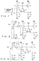
- FIG. 7 is a circuit diagram showing a reference voltage generation circuit according to a second embodiment of the present invention;
- FIG. 8 is a circuit diagram generally showing a reference voltage generation circuit of FIG. 7 with a starting circuit embodied as a practical form;
- FIG. 9 is a circuit diagram generally showing a reference voltage generation circuit of FIG. 7 with a starting circuit embodied as a practical form;
- FIG. 10 is a circuit diagram generally showing a reference voltage generation circuit of FIG. 7 with a starting circuit embodied as a practical form;
- FIG. 11 is a circuit diagram generally showing a reference voltage generation circuit of FIG. 7 with a starting circuit embodied as a practical form;
- FIG. 12 is a circuit diagram generally showing a reference voltage generation circuit of FIG. 7 with a starting circuit embodied as a practical form;
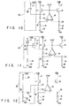
- FIG. 13 is a circuit diagram showing a reference voltage generation circuit according to a third embodiment of the present invention;
- FIG. 14 is a circuit diagram generally showing a reference voltage generation circuit of FIG. 13 with a starting circuit embodied as a practical form;
- FIG. 15 is a circuit diagram generally showing a reference voltage generation circuit of FIG. 13 with a starting circuit embodied as a practical form;
- FIG. 16 is a circuit diagram generally showing a reference voltage generation circuit of FIG. 13 with a starting circuit embodied as a practical form;
- FIG. 17 is a circuit diagram generally showing a reference voltage generation circuit of FIG. 13 with a starting circuit embodied as a practical form;
- FIG. 18 is a circuit diagram generally showing a reference voltage generation circuit of FIG. 13 with a starting circuit embodied as a practical form;
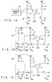
- FIG. 19 is a circuit diagram showing a reference voltage generation circuit according to a fourth embodiment of the present invention;
- FIG. 20 is a circuit diagram generally showing a reference voltage generation circuit of FIG. 19 with a starting circuit embodied as a practical form;
- FIG. 21 is a circuit diagram generally showing a reference voltage generation circuit of FIG. 19 with a starting circuit embodied as a practical form;
- FIG. 22 is a circuit diagram generally showing a reference voltage generation circuit of FIG. 19 with a starting circuit embodied as a practical form;
- FIG. 23 is a circuit diagram generally showing a reference voltage generation circuit of FIG. 19 with a starting circuit embodied as a practical form; and
- FIG. 24 is a circuit diagram generally showing a reference voltage generation circuit of FIG. 19 with a starting circuit embodied as a practical form.
- The embodiments of the present invention will be described below with reference to the accompanying drawings:
A reference voltage generation circuit according to a first embodiment of the present invention includes, as shown in FIG. 1, two NPN typebipolar transistors resistors input amplifier 16 andstarting circuit 30. - The collector of one
transistor 11 is connected to anode 17 supplied with a positive power supply potential VDD. One end of theresistor 13 is connected to the emitter of thetransistor 11. One end of theresistor 14 is connected to the other end of theresistor 13. The other end of theresistor 14 is connected to anode 18 supplied with a ground potential VSS. The collector of theother transistor 12 is connected to thenode 17. The base of thetransistor 12 is connected to that of thetransistor 11. One end of theresistor 15 is connected to the emitter of thetransistor 12. The other end of theresistor 15 is connected to thenode 18. - The differential-
input amplifier 16 has an inverting input terminal (-), non-inverting input terminal (+) and output terminal. The non-inverting input terminal (+) of theamplifier 16 is connected to aconnection node 19 between theresistors amplifier 16 is connected to aconnection node 20 between the emitter of thetransistor 12 and theresistor 15. - With the power supply ON, if a reference voltage Vref on the output terminal of the
amplifier 16 stays at a ground potential due to some causes, such as the effect of the input offset voltage of thedifferential input amplifier 16 and intrusion of noise, thestarting circuit 30 delivers an output close to a power supply potential VDD level to thenode 19. - In the reference voltage generation circuit of the present embodiment, a series circuit of the two
resistors transistor 11 and thenode 18 of a ground potential and theresistor 15 is connected between the emitter of thetransistor 12 and thenode 18 of the ground potential. By so doing, therespective transistors resistor 14 and one across theresistor 15 due to the emitter currents of thetransistors input amplifier 16. Further, the potential on the output terminal of the differential-input amplifier 16 is supplied to the respective bases of thetransistors input amplifier 16. - With the values of the
resistors transistor 12 by VBE and temperature voltages of thetransistors 

is obtained at an output terminal of the differential-input amplifier 16. - Let it be assumed that, in the reference voltage generation circuit of the above arrangement, there is no
such starting circuit 30. If, in this case, the output voltage Vref stays at a ground potential, at a time of starting an operation with the power supply ON, due to an input offset voltage of the differential-input amplifier 16, then thetransistors nodes - Since, in reality, the starting
circuit 30 is present, thenode 19 is placed, instead of staying at the ground potential as set out above, at a predetermined potential close to a power supply potential VDD due to the operation of the startingcircuit 30 after the power supply is rendered ON. At this time, current flows through theresistor 14 and a voltage drop occurs across theresistor 14, thus leading a rise in potential of thenode 19. Since the potential of thenode 19 is increased relative to the potential of thenode 20 to an extent that the input offset voltage of the differential-input amplifier 16 can be disregarded, the differential-input amplifier 16 performs a comparator operation and the output potential of the output terminal is raised. As a result, the base·emitter voltage VBE is applied to thetransistors transistors path comprising transistors input amplifier 16, it is possible to obtain a reference voltage Vref of a desired level finally given by theequation 1. - In the circuit of the present embodiment as shown in FIG. 1, the output potential of the starting
circuit 30 is supplied to the non-inverting input terminal of the differential-input amplifier 16, not to the bases of thetransistors input amplifier 16 be generated on the startingcircuit 30. It is therefore not necessary to increase the current drive capability of the starting circuit to such an extent as required in the prior art circuit. - Various forms of the starting
circuit 30 in the circuit of the present embodiment shown in FIG. 1 will be explained below by way of example. - A starting
circuit 30 as shown in FIG. 2 comprises a constantcurrent source 31,resistor 32 and NPN typebipolar transistor 33. One end of the constantcurrent source 31 is connected to thenode 17 of a power supply potential VDD and thetransistor 32 is connected between the other end of the constantcurrent source 31 and a ground potential VSS. The collector of thetransistor 33 is connected to thenode 17, the base of thetransistor 33 is connected to anode 34 of a series circuit of the constantcurrent source 31 andresistor 32 and the emitter of thetransistor 33 is connected to thenode 19. - In the reference voltage generation circuit having the starting
circuit 30 of such an arrangement, a predetermined bias potential greater than the base·emitter voltage VBE of thetransistor 33 is placed with respect to the emitter potential of thetransistor 33 after the power supply is turned ON. This state is achieved by setting the value of theresistor 32 and current value of the constantcurrent source 31. Even if the potential of thenode 19 stays at a ground potential after the power supply is turned ON, thetransistor 33 is turned ON through the supplying of the bias potential to the base of thetransistor 33. As a result, current flows in theresistor 14 via thetransistor 33 and a voltage drop occurs across theresistor 14. Thereafter, a differential-input amplifier 16 performs a comparator operation and a reference voltage Vref is delivered as an output signal from an output terminal. - When the reference voltage Vref becomes stable as the output, the potential of the
node 19 goes higher than a ground potential and a base·emitter voltage greater than VBE ceases being supplied to thetransistor 33. In consequence, thetransistor 33 is cut off and current flows through thetransistor 33, thus exerting no influence on thetransistor 11. - Even after the
transistor 33 is cut off, current continues flowing through the constantcurrent source 31. This current is consumed so long as a power supply potential is applied to an integrated circuit with the reference voltage generation circuit incorporated therein. Though the power supply potential is so applied to the integrated circuit, if there is no need to generate a reference voltage, it is possible to effectively achieve less power dissipation by making a dissipation current in the starting circuit 30 a zero. For this reason, a switch circuit which is ON-controlled by a power down signal is inserted in series with a current path of the constantcurrent source 31. In this case, it is only necessary that the startingcircuit 30 be operated by turning the switch circuit ON only when it is necessary to generate a reference voltage. - A starting
circuit 30 as shown in FIG. 3 is of such a type that aresistor 35 is used in place of the constantcurrent source 31 in the circuit shown in FIG. 2. In this case, a bias potential level emerging of anode 34 is set in accordance with a ratio of tworesistors - A starting
circuit 30 as shown in FIG. 4 is constructed of acapacitance 36 connected between thenode 17 of a power supply potential VDD and thenode 19. In a reference voltage generation circuit having such astarting circuit 30, when thenode 19 stays in a ground potential at a time of starting an operation after a power supply is rendered ON, a potential of thenode 19 is raised above the ground potential through the capacitive coupling made by thecapacitance 36. Thereafter, the potential of thenode 19 is increased to an extent that the offset voltage of a differential-input amplifier 16 can be disregarded. Thus, the differential-input amplifier 16 performs a comparator operation and its output voltage is raised. As a result, a base·emitter voltage VBE is applied totransistors transistors transistors input amplifier 16 allow a negative feedback operation and, finally, a reference voltage Vref is obtained as a desired predetermined level. - A starting
circuit 30 as shown in FIG. 5 is of such a type that an N channeltype MOS transistor 37 is employed in place of an NPN typebipolar transistor 33 in the circuit of FIG. 2. That is, the drain of theMOS transistor 37 is connected to thenode 17 of a power supply potential VDD, the source of theMOS transistor 37 to thenode 19 and the gate of theMOS transistor 37 to thenode 34. - In this case, the base·emitter voltage VBE of the NPN type
bipolar transistor 33 corresponds to the threshold voltage of the N-channeltype MOS transistor 37. That is, after the power supply is turned ON, the potential of thenode 34 is set to a predetermined bias potential relative to a source potential of theMOS transistor 37, the predetermined bias voltage being above the threshold voltage. This is realized by setting the value of aresistor 32 and current level of a constantcurrent source 31. Even in the case where a potential of thenode 19 stays at a ground potential after a power supply is turned ON, theMOS transistor 37 is turned ON through the application of the bias potential to the gate of the MOS transistor. Current flows in theresistor 14 through theMOS transistor 37 and a voltage drop occurs across theresistor 14. Thereafter, the differential-input amplifier 16 performs a comparator operation and a reference voltage Vref emerges as an output from an output terminal. - Further, when the output of the reference voltage Vref becomes stable, the potential of the
node 19 goes higher than a ground potential and no gate·source potential above the threshold voltage emerges on theMOS transistor 37. Thereafter, theMOS transistor 37 is cut off and no current flows in theMOS transistor 37 so that no influence is exerted on the current in atransistor 11. - A starting
circuit 30 as shown in FIG. 6 is of such a type that adiode 38 is used in place of the NPN typebipolar transistor 33 in the circuit shown in FIG. 2. In this case, the base·emitter voltage VBE of the NPN typebipolar transistor 33 corresponds to a forward drop voltage VF of thediode 38. That is, after a power supply is turned ON, a potential of themode 34 is set to a predetermined bias potential with respect to the cathode potential of thediode 38, the predetermined bias potential being above a forward drop voltage VF. That is realized by setting the values ofresistors node 19 stays at a ground potential, thediode 38 is turned ON through the application of the bias potential to the anode and current flows in theresistor 14 through thediode 38 and a voltage drop occurs across theresistor 14. Thereafter, the differential-input amplifier 16 performs a comparator operation and a reference voltage Vref is delivered as an output voltage from the output terminal. - A reference voltage generation circuit according to a second embodiment of the present invention as shown in FIG. 7 comprises, like the first embodiment of FIG. 1, two NPN type
bipolar transistors resistors input amplifier 16 and startingcircuit 30. However, the circuit of the second embodiment is different from that of the first embodiment in that, in the second embodiment, the output potential of the startingcircuit 30 is applied to aconnection node 21 between the emitter of thetransistor 11 and theresistor 13 instead of being applied to thenode 19. - In the first embodiment shown in FIG. 1, the potential of the
node 19 is raised to a level close to the power supply potential VDD by applying the output potential of the startingcircuit 30 to thenode 19. In the embodiment shown in FIG. 7, on the other hand, the same effect can be obtained by applying the output potential of the startingcircuit 30 to thenode 21, not to thenode 19. In this embodiment, the output voltage of the startingcircuit 30 is divided by tworesistors node 19, applied to the non-inverting input terminal of the differential-input amplifier 16. Therefore, since the potential of thenode 19 is lower than that in the embodiment shown in FIG. 1, the potential of thenode 19 can be raised up to a level adequately close to a power supply potential VDD. - Various practical variants of the starting
circuit 30 in the embodiment of FIG. 7 will be explained below. - As in the variant as shown in FIG. 2, a starting
circuit 30 shown in FIG. 8 comprises a constantcurrent source 31,resistor 32 and NPN typebipolar transistor 33. - As in the variant as shown in FIG. 3, a starting
circuit 30 shown in FIG. 9 uses aresistor 35 in place of the constantcurrent source 31 in the circuit shown in FIG. 8. - As in the variant shown in FIG. 4, a starting
circuit 30 shown in FIG. 10 is of such a type that it comprises acapacitance 36 connected between thenode 17 of a power supply potential VDD and thenode 21. - As in the variant shown in FIG. 5, a starting
circuit 30 shown in FIG. 11 uses an N channeltype MOS transistor 37 in place of the NPN typebipolar transistor 33 in the circuit shown in FIG. 8. - As in the variant shown in FIG. 6, a starting
circuit 30 shown in FIG. 12 uses adiode 38 in place of the NPN typebipolar transistor 33 in the circuit shown in FIG. 9. - A reference voltage generating circuit according to a third embodiment of the present invention shown in FIG. 13 uses PNP type
bipolar transistors bipolar transistors node 17 of a power supply potential VDD and thenode 18 of a ground potential VSS are connected in a reversed relation to those in the first embodiment shown in FIG. 1. In this embodiment, a startingcircuit 40 is provided in which, in the case where, after the turning ON of a power supply, a reference voltage Vref obtained as the output terminal of a differential-input amplifier 16 stays at a power supply potential due to some reasons, such as the input offset of the differential-input amplifier 16 and intrusion of noise, a startingcircuit 40 delivers a predetermined potential as an output close to a ground potential VSS to theconnection node 19 betweenresistors - Stated in another way, in the circuit of the embodiment, different currents flow through the two
PNP type transistors resistors input amplifier 16. In consequence, a potential on the output terminal of the differential-input amplifier 16 is applied to the bases of thetransistors input amplifier 16. - With, as in the case of FIG. 1, the values of
resistors transistor 23, by VBE, and the temperature voltages of thetransistors 

is obtained from the output terminal of the differential-input amplifier 16. - Let it be assumed that there is no starting
circuit 40 in the reference voltage generation circuit of the above arrangement. If, in this case, the output voltage Vref stays at a power supply potential, at the time of starting the operation after the turning ON of the power supply, due to the input offset voltage of the differential-input amplifier 16, no emitter current flows through the cutting off of both thetransistors - In reality, since the starting
circuit 40 is provided in the embodiment shown in FIG. 13, thenode 19 which might otherwise stay at the power supply potential as set out above is set to a potential close to a ground potential VSS through the operation of the startingcircuit 40 after the turning ON of the power supply. When this occurs, current is flowed through theresistor 14 and a voltage drop occurs across theresistor 14 and thus a potential drop occurs at thenode 19. With respect to the potential of thenode 20 the potential drop of thenode 19 is made greater to an extent that the offset voltage of the differential-input amplifier 16 can be disregarded. In consequence, the differential-input amplifier 16 performs a comparator operation and an output potential emerges, as a dropped one, from the output terminal. In consequence, the base·emitter voltage VBE is applied to thetransistors transistors transistors input amplifier 16, it is possible to obtain a reference voltage Vref of a desired level given by Equation 2. - Various practical variants of the starting
circuit 40 in the circuit according to the embodiment shown in FIG. 13 will be explained below. - The starting
circuit 40 as shown in FIG. 14 comprises a constantcurrent source 41,resistor 42 and PNP typebipolar transistor 43. One end of the constantcurrent source 41 is connected to thenode 18 of a ground potential VSS and theresistor 42 is connected between the other end of the constantcurrent source 41 and thenode 17 of a power supply potential VDD. The collector of thetransistor 43 is connected to thenode 18, the emitter of thetransistor 43 to thenode 19 and the base of thetransistor 43 to aconnection node 44 between the constantcurrent source 41 and theresistor 42. - In the reference voltage generation circuit having the starting
circuit 40 of such an arrangement, after the turning ON of the power supply, the potential of thenode 44 is set to a predetermined bias potential lower by over the base·emitter voltage VBE level than the emitter potential of thetransistor 43. This is realized by setting the value of theresistor 42 and current value of the constantcurrent source 41. Even in the case where the potential of thenode 19 stays at the power supply potential after the turning ON of the power supply, thetransistor 43 is turned ON through the application of a bias potential of thenode 44 to the base of the transistor and, through thetransistor 43, current flows through theresistor 14 to allow a voltage drop to occur across theresistor 14. Thereafter, a differential-input amplifier 16 performs a comparator operation and a reference voltage Vref emerges as an output voltage from the output terminal. - When the reference voltage Vref as the output voltage becomes stable, the potential of the
node 19 becomes lower than the power supply potential and no base·emitter voltage above VBE ceases being applied to thetransistor 43. Thus thetransistor 43 is cut off and no current flows there. In consequence, no influence is exerted on a current flowing in atransistor 22. - Even after the
transistor 43 is cut off, current flows in the constantcurrent source 41 and continues dissipated so long as a power supply potential is applied to an integrated circuit with the reference voltage generating circuit incorporated therein. Though the power supply potential is so supplied to the integrated circuit, if there is no need to generate the reference voltage, it is possible to effectively achieve less dissipation current by making a dissipation current in the starting current a zero. To this end, a switch circuit ON-controlled by a power down control signal is connected in series with a current path of the constantcurrent source 41. In this case, it is only necessary that, only when there is a need to generate a reference voltage, the startingcircuit 40 be operated by turning the switch circuit ON. - A starting
circuit 40 as shown in FIG. 15 uses aresistor 45 in place of the constantcurrent source 41 in the circuit shown in FIG. 14. In this case, a bias potential on thenode 44 is set in accordance with a ratio of tworesistors - A starting
circuit 40 as shown in FIG. 16 comprises acapacitance 46 connected between thenode 18 of a ground potential VSS and thenode 19. In a reference voltage generation circuit having the startingcircuit 40, when thenode 19 stays at a power supply potential at the time of starting an operation after the turning ON of the power supply, a potential of thenode 19 is made lower than a power supply potential through a capacitive coupling made by acapacitance 46. Thereafter, the potential of thenode 19 is lowered, as in the above case, relative to the potential of thenode 20 to an extent that an offset voltage of a differential-input amplifier 16 can be disregarded. The differential-input amplifier 16 performs a comparator operation and the output voltage of the differential-input amplifier 16 is dropped. As a result, the base·emitter voltage VBE is applied totransistors transistors transistors input amplifier 16. It is, therefore, possible to finally obtain a reference voltage Vref of a desired given level. - A starting
circuit 40 as shown in FIG. 17 uses a P channeltype MOS transistor 47 in place of the PNP typebipolar transistor 43 in the circuit shown in FIG. 14. In the starting circuit, that is, the drain of theMOS transistor 47 is connected to thenode 18, the source of thetransistor 47 to thenode 19 and the gate of the transistor to thenode 44. In this case, the base·emitter voltage VBE of thebipolar transistor 43 corresponds to the threshold voltage of theMOS transistor 47. - A starting
circuit 40 as shown in FIG. 18 uses adiode 48 in place of the PNP typebipolar transistor 43 in the circuit shown in FIG. 14. In this case, the base·emitter voltage VBE of thebipolar transistor 43 corresponds to a forward drop voltage VF of thediode 48. - A reference voltage generation circuit according to a fourth embodiment of the present invention as shown in FIG. 19 comprises, as in the third embodiment of FIG. 13, two PNP type
bipolar transistors resistors input amplifier 16 and startingcircuit 40. The embodiment of FIG. 19 is different from that of FIG. 13 in that an output potential of its startingcircuit 40 is applied to thenode 24 between the emitter of thetransistor 22 and theresistor 13 instead of being connected to thenode 19. - In the embodiment shown in FIG. 13, the potential of the
node 19 is lowered to a level close to a ground potential VSS by connecting the output potential of the startingcircuit 40 directly to thenode 19. In the embodiment shown in FIG. 19, on the other hand, the same effect as in the third embodiment is obtained by applying the output potential of the startingcircuit 40 to theconnection node 24 between the emitter of thetransistor 22 and theresistor 13 instead of being applied to thenode 19. In this case, the output potential of the startingcircuit 40, being divided by theresistors input amplifier 16. The potential of thenode 19 is made higher than that in the embodiment of FIG. 13, but the potential of thenode 19 can be lowered enough close to a ground potential VSS. - Various practical variants of the starting
circuit 40 in the embodiment of FIG. 19 will be explained below. - As in the variant as shown in FIG. 14, a starting
circuit 40 of FIG. 20 comprises a constantcurrent source 41,resistor 42 and PNP typebipolar transistor 43. - As in the variant of FIG. 15, a starting
circuit 40 of FIG. 21 uses aresistor 45 in place of the constantcurrent source 41 in the circuit of FIG. 20. - As in the variant of FIG. 16, a starting
circuit 40 of FIG. 22 comprises acapacitance 46 connected between thenode 18 of a ground potential VSS and thenode 24. - As in the variant of FIG. 17, a starting
circuit 40 of FIG. 23 uses a P channeltype MOS transistor 47 in place of the PNP typebipolar transistor 43 in the circuit shown in FIG. 20. - As in the variant shown in FIG. 18, a starting
circuit 40 of FIG. 24 uses adiode 48 in place of the PNP typebipolar transistor 43 in the circuit shown in FIG. 21. - According to the present invention, a reference voltage generation circuit is provided which can stably operate at all times without being adversely affected even if there is a variation in the characteristic of elements, intrusion of noise.
Claims (21)
- A reference voltage generation circuit comprising:
a first node (17; 18) for receiving a first potential (VDD; VSS);
a second node (18; 17) for receiving a second potential (VSS; VDD) different in level from the first potential;
a first bipolar transistor (11; 22) having a collector connected to the first node, an emitter and a base;
a second bipolar transistor (12; 23) having a collector connected to the first node, an emitter, and a base connected to that of the first bipolar transistor to provide a common base connection node, and having the same polarity as that of the first bipolar transistor;
a first resistor (13) having one end connected to the emitter of the first bipolar transistor and the other end;
a second resistor (14) having one end connected to said other end of the first resistor and the other end connected to the second node;
a third resistor (15) having one end connected to the emitter of the second bipolar transistor and the other end connected to the second node; and
a differential-input amplifier (16) having a non-inverting input terminal connected to a connection node between the first resistor and the second resistor, an inverting input terminal connected to said one end of the third resistor and an output terminal connected to a common base connection node between the first and second bipolar transistors and generating a reference voltage as an output voltage; characterized by further comprising:
starting means (30; 40) for generating a third potential close to the first potential after a power supply is turned ON and for applying it to the connection node between the first resistor and the second resistor. - The reference voltage generating circuit according to claim 1, characterized in that the starting means (30; 40) comprises:
a third bipolar transistor (33; 43) having a collector connected to the first node, an emitter connected to a series connection node between the first and second resistors and a base, the third bipolar transistor having the same polarity as those of the first and second bipolar transistors, and
bias potential generating means (31, 32, 35; 41, 42, 45) for applying a predetermined bias potential to the base of the third bipolar transistor. - The reference voltage generating circuit according to claim 2, characterized in that the bias potential generating means (31, 32, 35; 41, 42, 45) comprises:
a current source (31; 41) having one end connected to the first node and the other end; and
a fourth resistor (32; 42) having one end connected to said other end of the current source and the other end connected to the second node, wherein
a bias potential is generated from a series connection node of the current source and said fourth resistor. - The reference voltage generation circuit according to claim 3, characterized in that the current source (31; 41) is comprised of a fifth resistor (35; 45).
- The reference voltage generation circuit according to claim 1, characterized in that the starting means (30; 40) is comprised of a capacitance (36; 46) having one end connected to the first node and the other end connected to a series connection node of the first and second resistors.
- The reference voltage generation circuit according to claim 1, characterized in that the starting means (30; 40) comprises:
a MOS transistor (37; 47) having a drain connected to the first node, a source connected to a series connection node of the first and second resistors, and a gate;
bias potential generating means (31, 32, 35; 41, 42, 45) for applying a predetermined bias potential to the gate of the MOS transistor. - The reference voltage generation circuit according to claim 1, characterized in that the starting means (30; 40) comprises:
a diode (38; 48) having a cathode connected to a series connection node of the first and second resistors and an anode; and
bias potential generating means (32, 35; 42, 45) for applying a predetermined bias potential to the anode of the diode. - The reference voltage generation circuit according to claim 7, characterized in that the bias potential generating means (32, 35; 42, 45) comprises:
a sixth resistor (35; 45) having one end connected to the first node and the other end connected to the anode of the diode; and
a seventh resistor (32; 42) having one end connected to the anode of the diode and the other end connected to the second node. - The reference voltage generation circuit according to claim 1, characterized in that
the first and second bipolar transistors (11, 12), each, are comprised of an NPN transistor; and
the first potential (VDD) of the first node (17) is higher in level than the second potential (VSS) of the second node (18). - The reference voltage generation circuit according to claim 1, characterized in that
the first and second bipolar transistors (22, 23), each, are comprised of a PNP transistor; and
the first potential (VSS) of the first node (18) is lower in level than the second potential (VDD) on the second node (17). - A reference voltage generation circuit comprising:
a first node (17; 18) for receiving a first potential (VDD; VSS);
a second node (18; 17) for receiving a second potential (VSS; VDD) different in level from the first potential;
a first bipolar transistor (11, 22) having a collector connected to the first node, an emitter and a base;
a second bipolar transistor (12; 23) having a collector connected to the first node, an emitter, and a base connected to that of the first bipolar transistor to provide a common base connection node, the second bipolar transistor having the same polarity as that of the first bipolar transistor;
a first resistor (13) having one end connected to the emitter of the first bipolar transistor and the other end;
a second resistor (14) having one end connected to said other end of the first resistor and the other end connected to the second node;
a third resistor (15) having one end connected to the emitter of the second bipolar transistor and the other end connected to the second node; and
a differential-input amplifier (16) having a non-inverting input terminal connected to a series connection node of the first and second resistors, an inverting input terminal connected to said one end of the third resistor, and an output terminal connected to the common base connection node of the first and second bipolar transistors and generating a reference voltage as an output voltage, characterized by further comprising:
starting means (30; 40) for generating a third potential close to the first potential after a power supply is turned ON and for delivering the third potential to a connection node between the emitter of the first transistor and the first resistor. - The reference voltage generating circuit according to claim 11, characterized in that the starting means (30; 40) comprises:
a third bipolar transistor (33, 43) having a collector connected to the first node, an emitter connected to a connection node between the emitter of the first bipolar transistor and the first node and a base, and having the same polarity as those of the first and second bipolar transistors; and
bias potential generating means (31, 32, 35; 41, 42, 45) for applying a predetermined bias potential to the base of the third bipolar transistor. - The reference voltage generation circuit according to claim 12, characterized in that the bias potential generation means (31, 32, 35; 41, 42, 45) comprises:
a current source (31; 41) having one end connected to the first node and the other end; and
a fourth resistor (32; 42) having one end connected to said other end of the current source and the other end connected to the second node; wherein
the bias potential is generated from a connection node between the current source and the fourth resistor. - The reference voltage generation circuit according to claim 13, characterized in that the current source (31; 41) is comprised of a fifth resistor (35; 45).
- The reference voltage generation circuit according to claim 11, characterized in that the starting means (30; 40) is comprised of a capacitance (36; 46) having one end connected to the first node and the other end connected to a connection node between the emitter of the first bipolar transistor and the first resistor.
- The reference voltage generation circuit according to claim 11, characterized in that the starting means (30; 40) comprises:
a MOS transistor (37; 47) having a drain connected to the first node, a source connected to a connection node between the emitter of the first and bipolar transistor and the first resistor, and a gate; and
bias potential generating means (31, 32; 41, 42) for applying a predetermined bias potential to the gate of the MOS transistor. - The reference voltage generation circuit according to claim 11, characterized in that the starting means (30; 40) comprises:
a diode (38; 48) having a cathode connected to a connection node between the emitter of the first bipolar transistor and the first resistor and an anode; and
bias potential generating means (32, 35; 42, 45) for applying a predetermined bias potential to the anode of the diode. - The reference voltage generation circuit according to claim 17, characterized in that the bias potential generating means (32, 35; 42, 45) comprises:
a sixth resistor (35; 45) having one end connected to the first node and the other end connected to the anode of the diode; and
a seventh resistor (32; 42) having one end connected to the anode of the diode and the other end connected to the second node. - The reference voltage generation circuit according to claim 11, characterized in that
the first and second bipolar transistors (11, 12), each, are comprised of an NPN transistor; and
the first potential (VDD) of the first node (17) is higher in level than the second potential (VSS) of the second node (18). - The reference voltage generation circuit according to claim 11, characterized in that
the first and second bipolar transistors (22, 23), each, are comprised of a PNP transistor; and
the first potential (VSS) of the first node (18) is lower in level than the second potential (VDD) of the second node (17). - A reference voltage generation circuit comprising:
a first node (17; 18) for receiving a first potential (VDD; VSS);
a second node (18; 17) for receiving a second potential (VSS; VDD) different in level from the first potential;
a first bipolar transistor (11, 22) having a collector connected to the first node, an emitter and a base;
a second bipolar transistor (12; 23) having a collector connected to the first node, an emitter, and a base connected to that of the first bipolar transistor to provide a common base connection node;
a first resistor (13) having one end connected to the emitter of the first bipolar transistor and the other end;
a second resistor (14) having one end connected to the other end of the first resistor and the other end connected to the second node;
a third resistor (15) having one end connected to the emitter of the second bipolar transistor and the other end connected to the second node; and
a differential-input amplifier (16) having a non-inverting input terminal connected to a connection node between the first and second resistors, an inverting input terminal connected to said one end of the third resistor, and an output terminal connected to the common base connection node of the first and second bipolar transistors and generating a reference voltage as an output voltage, and characterized by further comprising:
starting means (30; 40) for applying a predetermined voltage to the non-inverting input terminal of the differential input terminal so that, when the reference voltage of a normal level is not delivered from the output terminal of the differential input amplifier after a power supply is turned ON, a potential of the non-inverting input terminal of the differential-input amplifier is set higher than a potential of the inverting input terminal of the differential-input amplifier.
Applications Claiming Priority (2)
| Application Number | Priority Date | Filing Date | Title |
|---|---|---|---|
| JP242507/93 | 1993-09-29 | ||
| JP24250793A JP3313475B2 (en) | 1993-09-29 | 1993-09-29 | Reference voltage generation circuit |
Publications (1)
| Publication Number | Publication Date |
|---|---|
| EP0645687A2 true EP0645687A2 (en) | 1995-03-29 |
Family
ID=17090136
Family Applications (1)
| Application Number | Title | Priority Date | Filing Date |
|---|---|---|---|
| EP94114599A Withdrawn EP0645687A2 (en) | 1993-09-29 | 1994-09-16 | Reference voltage generation circuit |
Country Status (3)
| Country | Link |
|---|---|
| EP (1) | EP0645687A2 (en) |
| JP (1) | JP3313475B2 (en) |
| KR (1) | KR950010338A (en) |
Cited By (1)
| Publication number | Priority date | Publication date | Assignee | Title |
|---|---|---|---|---|
| DE102006031549A1 (en) * | 2006-07-07 | 2008-01-31 | Infineon Technologies Ag | A bandgap reference circuit having a start-up circuit and a method of starting up a bandgap reference circuit |
-
1993
- 1993-09-29 JP JP24250793A patent/JP3313475B2/en not_active Expired - Fee Related
-
1994
- 1994-09-16 EP EP94114599A patent/EP0645687A2/en not_active Withdrawn
- 1994-09-28 KR KR1019940024492A patent/KR950010338A/en not_active Application Discontinuation
Cited By (3)
| Publication number | Priority date | Publication date | Assignee | Title |
|---|---|---|---|---|
| DE102006031549A1 (en) * | 2006-07-07 | 2008-01-31 | Infineon Technologies Ag | A bandgap reference circuit having a start-up circuit and a method of starting up a bandgap reference circuit |
| US7911195B2 (en) | 2006-07-07 | 2011-03-22 | Infineon Technologies Ag | Electronic circuits and methods for starting up a bandgap reference circuit |
| DE102006031549B4 (en) * | 2006-07-07 | 2016-08-04 | Infineon Technologies Ag | A method of operating a startup circuit for a bandgap reference circuit, methods of assisting startup of a bandgap reference circuit, and electronic circuitry for performing the methods |
Also Published As
| Publication number | Publication date |
|---|---|
| KR950010338A (en) | 1995-04-28 |
| JPH0798614A (en) | 1995-04-11 |
| JP3313475B2 (en) | 2002-08-12 |
Similar Documents
| Publication | Publication Date | Title |
|---|---|---|
| EP0372956B1 (en) | Constant current source circuit | |
| EP0601540A1 (en) | Reference voltage generator of a band-gap regulator type used in CMOS transistor circuit | |
| JPH08288804A (en) | Comparator circuit | |
| JP3001014B2 (en) | Bias voltage generation circuit | |
| US4647841A (en) | Low voltage, high precision current source | |
| EP0639894B1 (en) | Circuit for limiting the maximum current supplied to a load by a power transistor | |
| EP0117180B1 (en) | Differential switching circuit | |
| USRE37876E1 (en) | Power supply switch reference circuitry | |
| EP0645687A2 (en) | Reference voltage generation circuit | |
| US5349307A (en) | Constant current generation circuit of current mirror type having equal input and output currents | |
| EP0504559B1 (en) | Clamping circuit | |
| US5764105A (en) | Push-pull output circuit method | |
| US5063310A (en) | Transistor write current switching circuit for magnetic recording | |
| US5939907A (en) | Low power, high speed driving circuit for driving switching elements | |
| EP0323999A1 (en) | Level conversion circuit | |
| US4820967A (en) | BiCMOS voltage reference generator | |
| JP2729001B2 (en) | Reference voltage generation circuit | |
| KR100452176B1 (en) | Current Source - Short Circuit | |
| JP2900521B2 (en) | Reference voltage generation circuit | |
| JP3380308B2 (en) | Optical semiconductor relay device | |
| JPH0413692Y2 (en) | ||
| JPH05252019A (en) | Level conversion circuit | |
| JP3526484B2 (en) | High input impedance circuit | |
| JP3042471B2 (en) | Interface circuit | |
| JPH05343933A (en) | Voltage-current conversion circuit |
Legal Events
| Date | Code | Title | Description |
|---|---|---|---|
| PUAI | Public reference made under article 153(3) epc to a published international application that has entered the european phase |
Free format text: ORIGINAL CODE: 0009012 |
|
| 17P | Request for examination filed |
Effective date: 19940916 |
|
| AK | Designated contracting states |
Kind code of ref document: A2 Designated state(s): DE FR GB |
|
| STAA | Information on the status of an ep patent application or granted ep patent |
Free format text: STATUS: THE APPLICATION HAS BEEN WITHDRAWN |
|
| 18W | Application withdrawn |
Withdrawal date: 19960229 |
|
| R18W | Application withdrawn (corrected) |
Effective date: 19960229 |