EP0644590B1 - Method for planarizing a semiconductor surface and devices manufactured by the method - Google Patents
Method for planarizing a semiconductor surface and devices manufactured by the method Download PDFInfo
- Publication number
- EP0644590B1 EP0644590B1 EP94305590A EP94305590A EP0644590B1 EP 0644590 B1 EP0644590 B1 EP 0644590B1 EP 94305590 A EP94305590 A EP 94305590A EP 94305590 A EP94305590 A EP 94305590A EP 0644590 B1 EP0644590 B1 EP 0644590B1
- Authority
- EP
- European Patent Office
- Prior art keywords
- portions
- granular
- layer
- support structure
- insulators
- Prior art date
- Legal status (The legal status is an assumption and is not a legal conclusion. Google has not performed a legal analysis and makes no representation as to the accuracy of the status listed.)
- Expired - Lifetime
Links
Images







Classifications
-
- H—ELECTRICITY
- H10—SEMICONDUCTOR DEVICES; ELECTRIC SOLID-STATE DEVICES NOT OTHERWISE PROVIDED FOR
- H10P—GENERIC PROCESSES OR APPARATUS FOR THE MANUFACTURE OR TREATMENT OF DEVICES COVERED BY CLASS H10
- H10P95/00—Generic processes or apparatus for manufacture or treatments not covered by the other groups of this subclass
- H10P95/06—Planarisation of inorganic insulating materials
- H10P95/062—Planarisation of inorganic insulating materials involving a dielectric removal step
-
- H—ELECTRICITY
- H10—SEMICONDUCTOR DEVICES; ELECTRIC SOLID-STATE DEVICES NOT OTHERWISE PROVIDED FOR
- H10P—GENERIC PROCESSES OR APPARATUS FOR THE MANUFACTURE OR TREATMENT OF DEVICES COVERED BY CLASS H10
- H10P95/00—Generic processes or apparatus for manufacture or treatments not covered by the other groups of this subclass
- H10P95/06—Planarisation of inorganic insulating materials
-
- H—ELECTRICITY
- H10—SEMICONDUCTOR DEVICES; ELECTRIC SOLID-STATE DEVICES NOT OTHERWISE PROVIDED FOR
- H10W—GENERIC PACKAGES, INTERCONNECTIONS, CONNECTORS OR OTHER CONSTRUCTIONAL DETAILS OF DEVICES COVERED BY CLASS H10
- H10W20/00—Interconnections in chips, wafers or substrates
- H10W20/01—Manufacture or treatment
- H10W20/071—Manufacture or treatment of dielectric parts thereof
- H10W20/092—Manufacture or treatment of dielectric parts thereof by smoothing the dielectric parts
-
- H—ELECTRICITY
- H10—SEMICONDUCTOR DEVICES; ELECTRIC SOLID-STATE DEVICES NOT OTHERWISE PROVIDED FOR
- H10P—GENERIC PROCESSES OR APPARATUS FOR THE MANUFACTURE OR TREATMENT OF DEVICES COVERED BY CLASS H10
- H10P14/00—Formation of materials, e.g. in the shape of layers or pillars
- H10P14/60—Formation of materials, e.g. in the shape of layers or pillars of insulating materials
- H10P14/63—Formation of materials, e.g. in the shape of layers or pillars of insulating materials characterised by the formation processes
- H10P14/6326—Deposition processes
- H10P14/6328—Deposition from the gas or vapour phase
- H10P14/6334—Deposition from the gas or vapour phase using decomposition or reaction of gaseous or vapour phase compounds, i.e. chemical vapour deposition
-
- H—ELECTRICITY
- H10—SEMICONDUCTOR DEVICES; ELECTRIC SOLID-STATE DEVICES NOT OTHERWISE PROVIDED FOR
- H10P—GENERIC PROCESSES OR APPARATUS FOR THE MANUFACTURE OR TREATMENT OF DEVICES COVERED BY CLASS H10
- H10P14/00—Formation of materials, e.g. in the shape of layers or pillars
- H10P14/60—Formation of materials, e.g. in the shape of layers or pillars of insulating materials
- H10P14/63—Formation of materials, e.g. in the shape of layers or pillars of insulating materials characterised by the formation processes
- H10P14/6326—Deposition processes
- H10P14/6342—Liquid deposition, e.g. spin-coating, sol-gel techniques or spray coating
-
- H—ELECTRICITY
- H10—SEMICONDUCTOR DEVICES; ELECTRIC SOLID-STATE DEVICES NOT OTHERWISE PROVIDED FOR
- H10P—GENERIC PROCESSES OR APPARATUS FOR THE MANUFACTURE OR TREATMENT OF DEVICES COVERED BY CLASS H10
- H10P14/00—Formation of materials, e.g. in the shape of layers or pillars
- H10P14/60—Formation of materials, e.g. in the shape of layers or pillars of insulating materials
- H10P14/69—Inorganic materials
- H10P14/692—Inorganic materials composed of oxides, glassy oxides or oxide-based glasses
- H10P14/6921—Inorganic materials composed of oxides, glassy oxides or oxide-based glasses containing silicon
- H10P14/69215—Inorganic materials composed of oxides, glassy oxides or oxide-based glasses containing silicon the material being a silicon oxide, e.g. SiO2
-
- Y—GENERAL TAGGING OF NEW TECHNOLOGICAL DEVELOPMENTS; GENERAL TAGGING OF CROSS-SECTIONAL TECHNOLOGIES SPANNING OVER SEVERAL SECTIONS OF THE IPC; TECHNICAL SUBJECTS COVERED BY FORMER USPC CROSS-REFERENCE ART COLLECTIONS [XRACs] AND DIGESTS
- Y10—TECHNICAL SUBJECTS COVERED BY FORMER USPC
- Y10S—TECHNICAL SUBJECTS COVERED BY FORMER USPC CROSS-REFERENCE ART COLLECTIONS [XRACs] AND DIGESTS
- Y10S148/00—Metal treatment
- Y10S148/025—Deposition multi-step
Definitions
- the present invention relates to semiconductor devices including a semiconductor substrate with stepwise differences on the upper surface thereof, and to methods for fabricating such semiconductor devices.
- Semiconductor devices of high integration such as LSIs, VLSIs, etc., generally have a so-called multi-wiring layer structure having an n-th wiring layer formed by providing one or more wiring portions in a layer on a substrate, and further an n+1-th wiring layer formed through an insulating layer.
- Insulating layers, or inter-layer insulating layers, included in such multi-wiring layer structures have the intrinsic purpose of providing insulation between upper and lower layers (between a substrate and an adjacent wiring layer or between two adjacent wiring layers), and in addition the purpose of covering smoothly the rough substrate or wiring layers having stepwise differences on the upper surface thereof so as to provide a more planar surface (planarization).
- steps on surfaces of formed devices may be large, and wires may have to be thickened to compensate for lower wiring capacities due to the reduced size (micronization) of the wiring. Taking it into consideration that steps resulting from such wiring tend to be larger, it is necessary to ensure planarization of inter-film insulating films in forming multi-layer wirings.
- Previously-considered methods for forming an inter-layer insulating film include: a method (a) for forming an SiO 2 film on the surface of a substrate by CVD using a compound gas, such as SiH 4 or others, a method (b) for forming a CVD film using ozone-TEOS (tetraethoxy silane), a method (c) for forming an SOG (spin on glass) film by solving SiO x in a solvent, such as alcohol or others, and applying the SiO x to the surface of a substrate, and other methods.
- a method for forming an SiO 2 film on the surface of a substrate by CVD using a compound gas, such as SiH 4 or others a method (b) for forming a CVD film using ozone-TEOS (tetraethoxy silane), a method (c) for forming an SOG (spin on glass) film by solving SiO x in a solvent, such as alcohol or others, and applying the SiO x
- a first spin-on glass layer containing a ceramic filler is applied so as to cover the wiring portions and exposed portions of an underlying insulating film.
- the first SOG layer is then subjected to thermocuring.
- a further SOG layer is then applied over the first SOG layer to planarise the surface.
- the ceramic filler in the first SOG layer may be considered to provide granular insulators in that layer, but the layer is present over the wiring portions as well as over the underlying film in the finished device.
- the planarising effect of the first SOG layer containing the ceramic filler is incomplete.
- a semiconductor device comprising: a support structure including a semiconductor substrate, the said support structure having a substantially flat base layer and a wiring layer, including one or more wiring portions, formed on the said base layer, so that the support structure has an uneven face with first portions of a first level, provided respectively by portions of the base layer where the wiring portions are not present, and with second portions, between such first portions, of a second level that is higher than the said first level, which second portions are provided respectively by the wiring portions; characterised by granular insulators arranged, and fixed in place, over the said first portions of the said uneven face but not present over the said second portions thereof, the granular insulators being of such size, relative to the difference between the said first and second levels, that they serve with the second portions to provide a support surface, flatter than the said uneven face, for supporting a further layer of the device.
- granular insulators are provided in the concavities of the semiconductor structure (i.e. over the first portions of the uneven face), whereby steps not only in narrow regions between wires, but also in the entire region across the support structure can be eliminated, and higher degrees of global planarization can be obtained.
- the granular insulators are adhered to the semiconductor substrate through a spin on glass film. In this way, the granular insulators in the concavities are not displaced.
- the semiconductor device further comprises an insulating film covering the convexities (second portions) and concavities (first portions) in the uneven face of the support structure, and the granular insulators are disposed on the insulating film in the concavities of the uneven face.
- the device further comprises an insulating film covering the granular insulators. As a result, higher degrees of global planarization can be obtained.
- the semiconductor device further comprises another insulating film covering the granular insulators. As a result, higher degrees of global planarization can be obtained.
- the semiconductor device further comprises a spin on glass film covering the granular insulators. In this way, higher degrees of global planarization can be obtained.
- the granular insulator has a particle size above 0.3 times a step formed by the concavities and below 1.5 times the same.
- a particle diameter of the granular insulator is above 0.3 times and below 1.5 times the steps or stepwise differences formed by concavities, global steps can be sufficiently planarized.
- a method of fabricating a semiconductor device comprising: a granular insulator laying step of laying granular insulators over an uneven face of a support structure, the said support structure having a substantially flat base layer and a wiring layer, including one or more wiring portions, formed on the said base layer, so that the said uneven face has first portions of a first level, provided respectively by portions of the base layer where the wiring portions are not present, and second portions, between such first portions, of a second level that is higher than the said first level, which second portions are provided respectively by the wiring portions; a granular insulator removing step of removing the granular insulators over the said second portions of the said uneven face whilst leaving them over the said first portions thereof, the granular insulators being of such size, relative to the difference between the said first and second levels, that they serve with the said second portions to provide a support surface, flatter than the said uneven face, for supporting a further layer of the device; and a
- Such a method for fabricating a semiconductor device can eliminate steps not only in narrow regions between wires, but also across the entire region of the support structure to thereby planarize the support structure.
- granular insulators are laid over an entire upper surface of the support structure to provide the granular insulators in cavities on the upper surface of the support structure, and the granular insulators provided on convexities on the upper surface of the support structure are removed, whereby the concavities are buried with the granular insulators so as to improve global planarization.
- the method comprises: an SOG film applying step of applying an SOG film onto the upper surface of the support structure before the granular insulators laying step; and an SOG film heat treating step of heat treating the SOG film after the granular insulator laying step to adhere the granular insulators to the support structure through the SOG film.
- an SOG film is applied to a support structure before the granular insulators laying step, and the SOG film is heat treated after the granular insulators laying step, whereby the granular insulators are adhered to the support structure through the SOG film, and displacement of the granular insulators in the concavities can be prohibited.
- the method comprises: an SOG film applying step of applying the SOG film onto the granular insulators after the granular insulators laying step; and an SOG film heat treating step of heat treating the SOG film after the SOG film applying step to adhere the granular insulators to the support structure through the SOG film.
- an SOG film is applied onto the granular insulators after the granular insulators laying step, and the SOG film is heat treated after the SOG film applying step, whereby the granular insulators are adhered to the support structure through the SOG film.
- the method comprises: a lift-off layer forming step of forming a lift-off layer on the support structure before the granular insulators laying step, the granular insulators removing step being for removing the lift-off layer to remove the granular insulators.
- a lift-off layer is formed on a support structure before the granular insulators laying step, and lifting off the lift-off layer, whereby the granular insulators on the convexities can be easily removed.
- the lift-off layer is formed of a resist.
- the granular insulators on the convexities can be easily removed by lifting off without additional step.
- the lift-off layer is formed of amorphous carbon.
- the granular insulators removing step is performed by scraping the upper surface of the support structure to remove the granular insulators.
- the granular insulators on the convexities can be easily removed by scraping them off the upper surface of the support structure.
- the granular insulators removing step is performed by polishing the support structure to remove the granular insulators.
- the granular insulators on the convexities can be easily removed by such polishing (abrading).
- the method further comprises a silicon oxide film forming step of forming a silicon oxide film at the entire uneven face of the support structure before the granular insulators laying step; and a heat treating step of heat treating the granular insulators to adhere the granular insulators to the support structure after the granular insulators laying step.
- a silicon oxide film is formed onto the upper surface of the support structure before the granular insulators laying step, and the granular insulators are heat treated after the granular insulators laying step, whereby the granular insulators are adhered to the support structure.
- JP-A-6-097298 which is a document forming part of the state of the art only for certain claims of the present application not entitled to the priority date of 20th September 1993, discloses a method of forming an interlayer insulating film which employs an SOG film containing ceramic filler whose grain diameter is in the range from 0.5 to 1.5 times the thickness of the wiring portions.
- the SOG film is applied over the wiring portions and over the exposed portions of the underlying insulating layer by a spin coater or a roll coater such that the ceramic filler remains over the insulating layer but not over the wiring portions.
- the support structure does not have an insulating film that provides the entire uneven face of the support structure.
- FIGs. 1 to 3 A semiconductor device and a method for fabricating the semiconductor device according to a first embodiment of the present invention will be explained with reference to FIGs. 1 to 3.
- the semiconductor device includes a silicon wafer (semiconductor substrate) 11 on which devices are fabricated and an insulating layer such as SiO are formed on the surface except the bonding or electrode portion, a wiring layer (convexity) 12 formed on the silicon wafer 11, and silica particles 15 (granular insulators) disposed in concavities 14 between each aluminium wire 13 and its adjacent one in the wiring layer 12.
- a silicon wafer semiconductor substrate
- an insulating layer such as SiO are formed on the surface except the bonding or electrode portion
- a wiring layer (convexity) 12 formed on the silicon wafer 11
- silica particles 15 granular insulators
- This semiconductor device has the so-called multi-layer wiring structure having a plurality of wiring layers 12 (one of them shown) on the silicon wafer 11.
- the aluminium wires 13 are formed in a 1 ⁇ m wiring thickness and a 1 ⁇ m minimum wiring width, and at a 1 ⁇ m minimum inter-wire interval or space.
- Concavities 14 are formed between each aluminium wire 13 and its adjacent one 13.
- the concavities 14 have a step in level between the upper surface of the aluminium wires 13 and the surface of the silicon wafer 11.
- the wires 13 and underlying layers thus constitute a support structure, including the semiconductor substrate 11 and having an uneven face that has first portions 14 of a first level and second portions 13, between the first portions 13, of a second level that is higher than the first level.
- the silica particles 15 have a 0.8 ⁇ m diameter which is a little shorter than a wiring thickness (corresponding to the step between the aluminium wires 13 and the silicon wafer 11) of the aluminium wires 13 and are buried in the concavities 14 without any gap or space, i.e., in the gaps between each aluminium wires 13 and its adjacent one 13.
- the silica particles 15 are adhered to the silicon wafer 11 through an SOG film 16.
- silica particles are adhered, through an SOG film, to an inter-layer insulating film formed on a wiring layer positioned below (a lower wiring layer).
- the silica particles 15 can planarize the wiring layer 12 even when the wiring layer 12 as the next lower layer is rough.
- a silicon oxide film (SiO 2 film) 17 is formed on the silica particles 15 and the aluminium wires 13 over the entire silicon wafer 11.
- the semiconductor device 10 of the multi-layer wiring structure can eliminate the so-called global steps to thereby sufficiently planarize not only the regions between the wires but also the entire surface of the wiring layer 12, which is to be a next lower layer.
- FIGs. 2 and 3 are views explanatory of the method for fabricating a semiconductor device.
- aluminium (Al) is sputtered on the silicon wafer 11 in a about 1 ⁇ m-thickness.
- a resist 18 is applied to the entire surface of the aluminium layer 13, and the resist 18 is patterned in a pattern required wiring patterns such as fine pattern of 1 ⁇ m line and space, and wide patterns or plane patterns.
- the aluminium layer 13 is etched, and aluminium wires of a 1 ⁇ m wire thickness and a 1 ⁇ m minimum wire width, and at a 1 ⁇ m minimum inter-wire interval (FIG. 2A).
- wiring layers with the aluminium wires 12 or 13 are formed on the silicon wafer 11.
- inorganic SOG to be reflowed at about 200 °C is applied in an about 0.1 ⁇ m thickness by spin coating to the silicon wafer 11 with the aluminium wires 13 formed on, and the solvent is dried by means of a 150 °C hot plate. And an SOG film 16 is formed on the entire surface of the silicon wafer 11 including the aluminium wires 13 (FIG. 2B).
- a solution of 0.8 ⁇ m-diameter silica particles 15 dispersed in an MIBK (methylisobutyl ketone) solvent is applied to the entire upper surface of the silicon wafer without any gap by spin coating.
- the application of this solution positions the silica particles 15 in the cavities 14 defined between each aluminium wire 13 and its adjacent one 13 on the silicon wafer 11, and on the aluminium wires 13 through the SOG film 16 (FIG. 2C).
- the silicon wafer 11 is heated at 250 °C to bake the SOG film 16, so that the silica particles 15 are adhered to the upper surface of the silicon wafer 11 through the reflowed SOG film 16 (FIG. 3A).
- the resist 18 on the aluminum layer 13 on which the silica particles 15 is adhered is removed from the silicon wafer 11 with the silica particles adhered to. This removal of the resist 18 removes (lifts off) the silica particles 15 on the resist 18 together from the silicon wafer 11 together with the resist 18 (FIG. 3B).
- silica particles 15 buried in the cavities 14 between the aluminium wires 13 eliminate or planarise the steps between the aluminium wires 13 and the silicon wafer 11.
- the silicon wafer 11 after the lift-off process is rinsed with clean water.
- the silicon oxide film 17 is formed on the entire upper surface of the silicon wafer 11 by CVD (FIG. 3C).
- the silica particles 15 are left between aluminium wires 13, and none of the silica particles 15 are left on the aluminium wires 13,
- the entire upper surface of the wiring layer 12 is planarized by an inter-layer insulating film of silica particles 15 and the silicon oxide film 17. The so-called global steps can be eliminated.
- FIGs. 4 and 5 A semiconductor device and a method for fabricating the semiconductor device according to a second embodiment of the present invention will be explained with reference to FIGs. 4 and 5.
- the SOG film 16 is not formed on the upper surface of the silicon wafer 11 before the silica particles 15 are laid, but is formed after the silica particles 15 are laid.
- FIGs. 4 and 5 are views explanatory of the steps of the method for fabricating the semiconductor device 10.
- First aluminium (Al) is sputtered on the silicon wafer 11 in a about 1 ⁇ m-thickness. Then a resist 18 is applied to the entire surface of the aluminium layer 13 or substrate 11, and the resist 18 is patterned in a required wiring pattern. Using the patterned resist 18, the aluminium layer 13 is etched, and aluminium wires of a 1 ⁇ m wire thickness and a 1 ⁇ m minimum wire width, and at a 1 ⁇ m minimum inter-wire interval (FIG. 4A).
- a solution of 0.8 ⁇ m-diameter silica particles 15 dispersed in an MIBK (methylisobutyl ketone) solvent is applied to the entire upper surface of the silicon wafer without any gap or space by spin coating.
- the application of the solution positions the silica particles 15 in cavities 14 defined between the aluminium wires 13 on the silicon wafer 11 and the aluminium wires 13, and on the aluminium wires 13 without any gap (FIG. 4B).
- inorganic SOG to be reflowed at about 200 °C is applied by spin coating in an about 0.1 ⁇ m thickness to the silicon wafer 11 with the silica particles 15 laid on, and then the solvent is dried by a hot plate at 150 °C.
- the silicon wafer 11 is heated at 250 °C to bake the SOG film 16, so that the silica particles 15 are adhered to the upper surface of the silicon wafer 11 through the reflowed SOG film 16.
- the resist 18 is removed from the silicon wafer 11 with the silica particles adhered to. This removal of the resist 18 removes the silica particles 15 on the resist 18 from the silicon wafer 11 together with the resist 18 (FIG. 5A).
- silica particles 15 buried in the cavities 14 between each aluminium wire 13 and its adjacent one eliminate steps defined between the aluminium wires 13 and the silicon wafer 11.
- a silicon oxide film 17 is formed on the entire surface of the silicon wafer 11 by CVD (FIG. 5B).
- the silica particles 15 are left between aluminium wires 13, and none of the silica particles 15 are left on the aluminium wires 13.
- the entire upper surface of the wiring layer 12 is planarized by an inter-layer insulating film of silica particles 15 and the silicon oxide film 17. The so-called global steps can be eliminated.
- the method for fabricating the semiconductor device according to the third embodiment is characterized that the silica particles 15 on the aluminium wires 13 are mechanically removed.
- the method according to the third embodiment is the same as that according to the first embodiment in the other constitution and function.
- FIG. 6 is views explanatory of the steps of the method for fabricating the semiconductor device 10.
- the third embodiment is substantially the same as the method according to the first embodiment for fabricating the semiconductor device 10 up to the step of laying silica particles 15 on the entire upper surface of a silicon wafer 11 including aluminium wires 13, and adhering the silica particles 15 to the silicon wafer 11 through an SOG film 16 (FIGs. 2A to 2C, FIG. 3A).
- the silica particles 15 are laid in the cavities 14 in the silicon wafer 11 and on the aluminium wires 13 without any gap through the SOG film 16, and the silica particles 15 are adhered to the upper surface of the silicon wafer 11 (FIG. 6A).
- a squeegee (abrasion means) 19 for abrading off the silica particles 15 on move along the wiring layer 12 completely removes the silica particles 15 and the resist 18 on the aluminium wires 13 (FIG. 6C).
- a silicon oxide film 17 is formed on the entire of the silicon wafer 11 by CVD (FIG. 6D).
- abrasion means (polishing means)20 which is moved on rotation over the wiring layer 12 to remove the silica particles 15 on the aluminium wires 13 may be used in place of the squeegee 19.
- the abrasion or polishing means 20 comprises a flexible body 21 having flexibility which allows the flexible body 21 to follow in required contact with the wiring layer 12 having the silica particles 15 to be removed, and an abrasive cloth 22 provided on the underside of the flexible body 21 in contact with the wiring layer 12, whereby the abrasion or polishing means 20 is moved on rotation over the wiring layer 12, so that the abrasive cloth 22 can remove the silica particles 15 laid upper of the upper surface of the aluminium wires 13.
- the flexible body 21 is in the form of, e.g., a pole or columnar of a rubber-like material, or uses a coil spring or others so that flexibility is imparted to the underside thereof, and is flexible enough to contact the abrasive cloth 22 with the wiring layer 12.
- the abrasive cloth 22 is provided by an abrasive material, such as alumina ceramics, glass or others, which does not damage the wiring layer 12 during the abrasion or polishing process.
- the granular insulators are provided by silica particles 15, but are not limited to them.
- the granular insulators may be particulate bodies of an insulator, such as aluminium nitride, titanium oxide, boron nitride or others as long as they can form an inter-layer insulating film and are buried in the cavities 14 to successfully eliminate the steps between the aluminium wires 13 and the silicon wafer 11. It is preferred that a particulate body is selected in consideration of a dispersion ratio thereof in MIBK solvents, and dielectric constants.
- a dielectric constant is below 4.5.
- the granular insulators are formed of a low-dielectric constant material, such as boron nitride, whereby a inter-layer capacitance of the aluminium wires 13 is lowered, whereby the semiconductor device can have higher speed.
- a particle diameter of the granular insulator is not limited to 0.8 ⁇ m in the above-described embodiments.
- a particle diameter may be above 0.3 times and below 1.5 times of a step between the silicon wafer 11 and the aluminium wires 13 for first wiring layer. Such size can effectively eliminate steps of the aluminium wires 13.
- the concavities and convexities on the upper surface of the semiconductor substrate 11 are formed by the aluminium wires and, in addition, by the electrodes, oxide films, etc.
- FIGs. 9 and 10 A method for fabricating a semiconductor device according to a fourth embodiment of the present invention will be explained with reference to FIGs. 9 and 10.
- aluminium (Al) is sputtered on a silicon wafer 11 to form an about 1 ⁇ m-thickness aluminium layer 13.
- carbon is sputtered on the entire surface of the aluminium layer 13 to form an about 60 nm-thickness amorphous carbon layer 30.
- a resist 18 is applied to the entire surface of the amorphous carbon layer 30, and the resist 18 is patterned in a required wiring pattern.
- the amorphous carbon layer 30 and the aluminium layer 13 are etched by using Cl 2 gas and BCl 3 gas.
- the aluminium wiring layer 13 with the amorphous carbon layer provided on has a 1 ⁇ m wire thickness, a 1 ⁇ m minimum wire width and a 1 ⁇ m minimum inter-wire interval (FIG. 9A).
- Etching rates of the resist and the amorphous carbon by the ashing apparatus using CF 4 gas and O 2 gas were measured under various conditions.
- the etching rate rises.
- the resist and the amorphous carbon can have sufficient etching selection ratio.
- amorphous carbon was not substantially etched.
- the resist 18 was selectively etched at about 115 °C.
- Inorganic SOG which reflows at about 200 °C was applied in an about 0.1 ⁇ m, by spin coat, to a silicon wafer having the amorphous carbon layer 30 and the aluminium wires 13, and then the solvent is dried by a hot plate at 150 °C.
- an SOG film 16 is formed on the upper surface of the silicon wafer 11 including the aluminium wires 13 and the amorphous carbon layer 30 (FIG. 9C).
- a solution of 0.8 ⁇ m-diameter silica particles 15 dispersed in MIBK (methylisobutyl ketone) solvent is applied to the entire upper surface of the silicon wafer 11 by spin coat to lay the silica particles without any gap.
- MIBK methylisobutyl ketone
- the silica particles 15 are laid without any gap in concavities defined between aluminium wires 13 on the silicon wafer 11, and on the amorphous carbon layer 30 through the SOG film 16 (FIG. 9D).
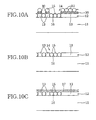
- the silicon wafer 11 is heated at 250 °C to be baked, so that the silica particles 15 are adhered to the upper surface of the silicon wafer 11 through the reflowed SOG film (FIG. 10A).
- the amorphous carbon layer 30 is removed from the silicon wafer 11 with the silica particles adhered to at a treating temperature above 200 °C by the above-described ashing apparatus.
- the removal of the amorphous carbon layer 30 removes (lifted off) the silica particles 15 on the amorphous carbon layer 30 from the silicon wafer 11 together with amorphous carbon layer 30 (FIG. 10B).
- the silica particles 15 in the concavities 14 between aluminium wires 13 eliminate steps between the aluminium wires 13 and the recesses 14.
- the silicon oxide film 17 is formed on the entire surface of the silicon wafer 11 (FIG. 10C).
- the resist is removed immediately following the patterning of the aluminium layer without leaving the resist for a long period of time. Consequently corrosion of the aluminium wires 13 due to residues based on hydrogen chloride used in the etching can be prevented.
- an SOG film 16 is formed on the upper surface of a silicon wafer 11 not before silica particles 15 are laid, but after the silica particles 15 are laid.
- aluminium (Al) is sputtered on a silicon wafer 11 to form an about 1 ⁇ m-thickness aluminium layer 13.
- carbon is sputtered on the entire surface of the aluminium layer 13 to form an about 60 nm-thickness amorphous carbon layer 30.
- a resist 18 is applied to the entire surface of the amorphous carbon layer 30, and the resist is patterned in a required wiring pattern.
- the amorphous carbon layer 30, and the aluminium layer 13 are plasma or dry etched by using Cl 2 gas and BCl 3 gas.
- aluminium wires 13 having a 1 ⁇ m wire thickness, a 1 ⁇ m minimum width and a 1 ⁇ m minimum inter-wire interval (FIG. 11A).
- the resist 18 is selectively etched at an about 115 °C treating temperature by the above-described ashing apparatus using CF 4 gas and O 2 gas (FIG. 11B).
- the inorganic SOG which reflows at an about 200 °C is applied in an about 0.1 ⁇ m thickness by spin coat on the silicon wafer 11 with the silica particles laid on, and then the solvent is vaporized by a hot plate of 150 °C.
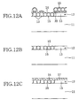
- the SOG film 16 having the silica particles 15 buried in the entire upper surface of the silicon wafer 11 is formed on the entire upper surface of the silicon water including the amorphous carbon layer 30 and the aluminium wires 13 (FIG. 12A).
- the silicon wafer 11 is heated at 250 °C to bake the SOG film 16, and the silica particles 15 are adhered to the upper surface of the silicon wafer 11 through the reflowed SOG film 16.
- the amorphous carbon layer 30 is removed, at a processing temperature above 200 °C by the above-described ashing apparatus, from the silicon wafer 11 with the silica particles 15 adhered to.
- the amorphous carbon layer 30 is removed (lifted off) to remove the amorphous carbon layer 30, and the silica particles on the amorphous carbon layer 30 from the silicon wafer 11 (FIG. 12B).
- the silica particles 15 buried in the concavities between the aluminium wires 13 eliminate steps between the aluminium wires 13 and the silicon wafer 11.
- the silicon oxide film 17 is formed on the entire surface of the silicon wafer 11 by CVD (FIG. 12C).
- the resist is removed immediately following patterning of the aluminium layer without leaving the resist for a long period of time. Accordingly generation corrosion of the aluminium wires 13 due to residues based on hydrogen chloride used in the etching can be prevented.
- a semiconductor device and a method for fabricating the semiconductor device according to a sixth embodiment of the present invention will be explained with reference to FIGs. 13 to 16.
- the semiconductor device has the so-called multi-layer wiring structure having a plurality of wiring layers 12 (one of them shown) on a silicon wafer 11.
- the wiring layer 12 includes aluminium wires (convexities) 13.
- Concavities 14 are formed between each aluminium wire 13 and its adjacent one 13.
- the concavities 14 have a depth of steps between the aluminium wires 13 and the silicon wafer 11.
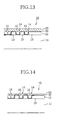
- a silicon oxide film 32 having a 50 nm thickness is formed on the aluminium wires 13 and the concavities 14 over the entire silicon wafer 11.
- Silica particles 15 are disposed on the silicon oxide film 32 in the concavities 14.
- the silica particles 15 have surfaces coated with thin SOG coatings (not shown).
- the silica particles 15 are adhered to the silicon oxide film 32 through the thin SOG coatings.
- the silica particles 15 can planarize the wiring layer 12 even when the wiring layer 12 as the next lower layer is rough.
- a silicon oxide film 33 by CVD is formed on the silica particles 15 and the silicon oxide film 32 over the entire silicon wafer 11.
- the semiconductor device 10 of the multi-layer wiring structure can eliminate the so-called global steps to thereby sufficiently planarize not only the regions between the wires but also the entire surface of the wiring layer 12, which is to be a next lower layer.
- FIG. 14 is a view of another example of the semiconductor device according to the sixth embodiment.
- a SOG film 34 in place of the silicon oxide film 33 is formed on the silica particles 15 and the silicon oxide film 32 over the entire silicon wafer 11.
- a wiring layer 12 with aluminium wires 13 is formed on a silicon wafer 11.
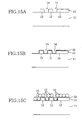
- the wiring layer 12 includes the aluminium wires 13 in a 1 ⁇ m minimum wire width at a 1 ⁇ m minimum inter-wire interval (FIG. 15A).
- a silicon oxide film 32 is formed on the aluminium wires 13 and concavities 14 over the entire silicon wafer 11 by CVD (FIG. 15B).
- silica particles 15 dispersed in MIBK (methylisobutyl ketone) solvent is applied to the upper surface of the silicon wafer 11 by spin coat to lay the silica particles 15 without any gap (FIG. 15C).
- the silica particles 15 have surfaces coated with thin SOG coatings (not shown).
- the silicon wafer 11 is heated at 250 °C to bake the thin SOG coatings on the surfaces of the silica particles 15, so that the silica particles 15 are adhered to the silicon oxide film 32 (FIG. 15C).
- a squeegee 19 for abrading off the silica particles 15 completely removes the silica particles 15 on the silicon oxide film 32 over the aluminium wires 13 (FIG. 6A).
- the silica particles 15 are disposed on the silicon oxide film 32 only in the concavities 14 to planarize the wiring layer 12.
- the abrasion or polishing means 20 shown in FIG. 7 which is moved on rotation over the silicon oxide film 32 to remove the silica particles 15 on the silicon oxide film 32 over the aluminium wires 13 may be used in place of the squeegee 19.
- a silicon oxide film 33 is formed on the silica particles 15 and the silicon oxide film 32 over the entire silicon wafer 11 by CVD (FIG. 16B).
- inorganic SOG to be reflowed at about 200 °C is applied in an about 0.1 ⁇ m thickness by spin coating over the silicon wafer 11, and the solvent is dried by means of a 150 °C hot plate. And an SOG film 34 is formed on the silica particles 15 and the silicon oxide film 32 over the entire silicon wafer 11 (FIG. 16C).
- the semiconductor device 10 of the multi-layer wiring structure can eliminate the so-called global steps to thereby sufficiently planarize not only the regions between the wires but also the entire surface of the wiring layer 12, which is to be a next lower layer.
- embodiments of the present invention can provide a semiconductor device whose support structure is sufficiently planarized with steps eliminated not only in narrow regions between wires, but also in an entire region across the support structure.
Landscapes
- Internal Circuitry In Semiconductor Integrated Circuit Devices (AREA)
Description
- The present invention relates to semiconductor devices including a semiconductor substrate with stepwise differences on the upper surface thereof, and to methods for fabricating such semiconductor devices.
- Semiconductor devices of high integration, such as LSIs, VLSIs, etc., generally have a so-called multi-wiring layer structure having an n-th wiring layer formed by providing one or more wiring portions in a layer on a substrate, and further an n+1-th wiring layer formed through an insulating layer.
- Insulating layers, or inter-layer insulating layers, included in such multi-wiring layer structures have the intrinsic purpose of providing insulation between upper and lower layers (between a substrate and an adjacent wiring layer or between two adjacent wiring layers), and in addition the purpose of covering smoothly the rough substrate or wiring layers having stepwise differences on the upper surface thereof so as to provide a more planar surface (planarization).
- In this respect, as integration of semiconductor integrated circuits is improved, steps on surfaces of formed devices may be large, and wires may have to be thickened to compensate for lower wiring capacities due to the reduced size (micronization) of the wiring. Taking it into consideration that steps resulting from such wiring tend to be larger, it is necessary to ensure planarization of inter-film insulating films in forming multi-layer wirings.
- This is because, if an inter-layer insulating film permits roughness of a lower layer (a substrate or a lower wiring layer) to be still present in an upper layer, there is a risk that breakage and/or defective insulation will occur at a wiring portion in the upper layer, and a margin of a focal depth of a resist in the wiring will be adversely narrowed, and integration of the wiring may be impaired.
- Previously-considered methods for forming an inter-layer insulating film include: a method (a) for forming an SiO2 film on the surface of a substrate by CVD using a compound gas, such as SiH4 or others, a method (b) for forming a CVD film using ozone-TEOS (tetraethoxy silane), a method (c) for forming an SOG (spin on glass) film by solving SiOx in a solvent, such as alcohol or others, and applying the SiOx to the surface of a substrate, and other methods.
- But in the method (a), roughness of a wiring itself is still present in an upper layer. A problem with the method (a) is that a formed inter-layer insulating film has very poor planarization.
- In the above-described methods (b) and (c), roughness in a region with small inter-wire gaps can be planarized by reflow, but steps (global steps) between regions without wirings formed or plane electrode layers such as ground electrode or power electrode layers, and regions with fine wirings formed densely, cannot be eliminated. This is a problem with the methods (b) and (c).
- In another method of forming an inter-layer insulating film, disclosed in JP-A-5-175194, a first spin-on glass layer containing a ceramic filler is applied so as to cover the wiring portions and exposed portions of an underlying insulating film. The first SOG layer is then subjected to thermocuring. As this first SOG layer does not planarise the surface sufficiently, a further SOG layer is then applied over the first SOG layer to planarise the surface. In this method, the ceramic filler in the first SOG layer may be considered to provide granular insulators in that layer, but the layer is present over the wiring portions as well as over the underlying film in the finished device. Thus, the planarising effect of the first SOG layer containing the ceramic filler is incomplete.
- According to a first aspect of the present invention there is provided a semiconductor device comprising: a support structure including a semiconductor substrate, the said support structure having a substantially flat base layer and a wiring layer, including one or more wiring portions, formed on the said base layer, so that the support structure has an uneven face with first portions of a first level, provided respectively by portions of the base layer where the wiring portions are not present, and with second portions, between such first portions, of a second level that is higher than the said first level, which second portions are provided respectively by the wiring portions; characterised by granular insulators arranged, and fixed in place, over the said first portions of the said uneven face but not present over the said second portions thereof, the granular insulators being of such size, relative to the difference between the said first and second levels, that they serve with the second portions to provide a support surface, flatter than the said uneven face, for supporting a further layer of the device.
- In such a device, granular insulators are provided in the concavities of the semiconductor structure (i.e. over the first portions of the uneven face), whereby steps not only in narrow regions between wires, but also in the entire region across the support structure can be eliminated, and higher degrees of global planarization can be obtained.
- In the above-described semiconductor device, it is preferable that the granular insulators are adhered to the semiconductor substrate through a spin on glass film. In this way, the granular insulators in the concavities are not displaced.
- In the above-described semiconductor device, it is preferable that the semiconductor device further comprises an insulating film covering the convexities (second portions) and concavities (first portions) in the uneven face of the support structure, and the granular insulators are disposed on the insulating film in the concavities of the uneven face. As a result, steps not only in narrow regions between wires, but also across the entire region of the support structure can be eliminated, and higher degrees of global planarization can be obtained.
- In the above-described semiconductor device, it is preferable that the device further comprises an insulating film covering the granular insulators. As a result, higher degrees of global planarization can be obtained.
- In the above-described semiconductor device, it is preferable that the semiconductor device further comprises another insulating film covering the granular insulators. As a result, higher degrees of global planarization can be obtained.
- In the above-described semiconductor device, it is preferable that the semiconductor device further comprises a spin on glass film covering the granular insulators. In this way, higher degrees of global planarization can be obtained.
- In the above-described semiconductor device, it is preferable that the granular insulator has a particle size above 0.3 times a step formed by the concavities and below 1.5 times the same. When a particle diameter of the granular insulator is above 0.3 times and below 1.5 times the steps or stepwise differences formed by concavities, global steps can be sufficiently planarized.
- According to a second aspect of the present invention there is provided a method of fabricating a semiconductor device, comprising: a granular insulator laying step of laying granular insulators over an uneven face of a support structure, the said support structure having a substantially flat base layer and a wiring layer, including one or more wiring portions, formed on the said base layer, so that the said uneven face has first portions of a first level, provided respectively by portions of the base layer where the wiring portions are not present, and second portions, between such first portions, of a second level that is higher than the said first level, which second portions are provided respectively by the wiring portions; a granular insulator removing step of removing the granular insulators over the said second portions of the said uneven face whilst leaving them over the said first portions thereof, the granular insulators being of such size, relative to the difference between the said first and second levels, that they serve with the said second portions to provide a support surface, flatter than the said uneven face, for supporting a further layer of the device; and a granular insulator fixing step of fixing the granular insulators in place over the first portions of the said uneven face.
- Such a method for fabricating a semiconductor device can eliminate steps not only in narrow regions between wires, but also across the entire region of the support structure to thereby planarize the support structure.
- In one such method first, granular insulators are laid over an entire upper surface of the support structure to provide the granular insulators in cavities on the upper surface of the support structure, and the granular insulators provided on convexities on the upper surface of the support structure are removed, whereby the concavities are buried with the granular insulators so as to improve global planarization.
- In one embodiment of the method for fabricating the semiconductor device, the method comprises: an SOG film applying step of applying an SOG film onto the upper surface of the support structure before the granular insulators laying step; and an SOG film heat treating step of heat treating the SOG film after the granular insulator laying step to adhere the granular insulators to the support structure through the SOG film. In this way, an SOG film is applied to a support structure before the granular insulators laying step, and the SOG film is heat treated after the granular insulators laying step, whereby the granular insulators are adhered to the support structure through the SOG film, and displacement of the granular insulators in the concavities can be prohibited.
- In another embodiment of the method, the method comprises: an SOG film applying step of applying the SOG film onto the granular insulators after the granular insulators laying step; and an SOG film heat treating step of heat treating the SOG film after the SOG film applying step to adhere the granular insulators to the support structure through the SOG film. In this way, an SOG film is applied onto the granular insulators after the granular insulators laying step, and the SOG film is heat treated after the SOG film applying step, whereby the granular insulators are adhered to the support structure through the SOG film.
- In another embodiment of the method, the method comprises: a lift-off layer forming step of forming a lift-off layer on the support structure before the granular insulators laying step, the granular insulators removing step being for removing the lift-off layer to remove the granular insulators. In this way, a lift-off layer is formed on a support structure before the granular insulators laying step, and lifting off the lift-off layer, whereby the granular insulators on the convexities can be easily removed.
- In the above-described method for fabricating the semiconductor device, it is preferable that the lift-off layer is formed of a resist. As a result, the granular insulators on the convexities can be easily removed by lifting off without additional step.
- Alternatively, it is preferable that the lift-off layer is formed of amorphous carbon. As a result, corrosion of aluminium wires due to residues based on hydrogen chloride used in the etching, which occurs when a resist is left on for a long period of time, can be prevented.
- In one embodiment the granular insulators removing step is performed by scraping the upper surface of the support structure to remove the granular insulators. The granular insulators on the convexities can be easily removed by scraping them off the upper surface of the support structure.
- In another embodiment the granular insulators removing step is performed by polishing the support structure to remove the granular insulators. The granular insulators on the convexities can be easily removed by such polishing (abrading).
- It is preferable that the method further comprises a silicon oxide film forming step of forming a silicon oxide film at the entire uneven face of the support structure before the granular insulators laying step; and a heat treating step of heat treating the granular insulators to adhere the granular insulators to the support structure after the granular insulators laying step. As a result, a silicon oxide film is formed onto the upper surface of the support structure before the granular insulators laying step, and the granular insulators are heat treated after the granular insulators laying step, whereby the granular insulators are adhered to the support structure.
- Incidentally, JP-A-6-097298, which is a document forming part of the state of the art only for certain claims of the present application not entitled to the priority date of 20th September 1993, discloses a method of forming an interlayer insulating film which employs an SOG film containing ceramic filler whose grain diameter is in the range from 0.5 to 1.5 times the thickness of the wiring portions. The SOG film is applied over the wiring portions and over the exposed portions of the underlying insulating layer by a spin coater or a roll coater such that the ceramic filler remains over the insulating layer but not over the wiring portions. In this method the support structure does not have an insulating film that provides the entire uneven face of the support structure.
- Reference will now be made, by way of example, to the accompanying drawings, in which:
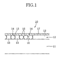
- FIG. 1 is a sectional view of the semiconductor device according to a first embodiment of the present invention.
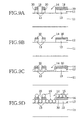
- FIGS. 2A to 2C are views of the steps of a method for fabricating the semiconductor device according to the first embodiment of the present invention.
- FIGS. 3A to 3C are views of the steps of the method for fabricating the semiconductor device according to the first embodiment of the present invention.
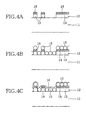
- FIGS. 4A to 4C are views of the steps of a method for fabricating the semiconductor device according to a second embodiment of the present invention.
- FIGS. 5A and 5B are views of the steps of the method for fabricating the semiconductor device according to the second embodiment of the present invention.
- FIGS. 6A to 6D are views of the steps of a method for fabricating the semiconductor device according to a third embodiment of the present invention.
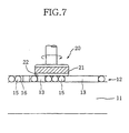
- FIG. 7 is a view of a step of another example of the method for fabricating the semiconductor device according to the third embodiment of the present invention.
- FIGS. 8A and 8B are views of relationships between particle diameters of silica particles and global steps.
- FIGS. 9A to 9D are views of the steps of a method for fabricating the semiconductor device according to a fourth embodiment of the present invention.
- FIGS. 10A to 10C are views of the steps of the method for fabricating the semiconductor device according to the fourth embodiment of the present invention.
- FIGS. 11A to 11C are views of the steps of a method for fabricating the semiconductor device according to a fifth embodiment of the present invention.
- FIGS. 12A to 12C are views of the steps of the method for fabricating the semiconductor device according to the fifth embodiment of the present invention.
- FIG. 13 is a sectional view of the semiconductor device according to a sixth embodiment of the present invention.
- FIG. 14 is a sectional view of another example of the semiconductor device according to the sixth embodiment of the present invention.
- FIGS. 15A to 15C are views of the steps of a method for fabricating the semiconductor device according to the sixth embodiment of the present invention.
- FIGS. 16A to 16C are views of the steps of the method for fabricating the semiconductor device according to the sixth embodiment of the present invention.
-
- A semiconductor device and a method for fabricating the semiconductor device according to a first embodiment of the present invention will be explained with reference to FIGs. 1 to 3.
- As shown in FIG. 1, the semiconductor device according to this embodiment includes a silicon wafer (semiconductor substrate) 11 on which devices are fabricated and an insulating layer such as SiO are formed on the surface except the bonding or electrode portion, a wiring layer (convexity) 12 formed on the
silicon wafer 11, and silica particles 15 (granular insulators) disposed inconcavities 14 between eachaluminium wire 13 and its adjacent one in thewiring layer 12. - This semiconductor device has the so-called multi-layer wiring structure having a plurality of wiring layers 12 (one of them shown) on the
silicon wafer 11. - The
aluminium wires 13 are formed in a 1 µm wiring thickness and a 1 µm minimum wiring width, and at a 1 µm minimum inter-wire interval or space.Concavities 14 are formed between eachaluminium wire 13 and itsadjacent one 13. Theconcavities 14 have a step in level between the upper surface of thealuminium wires 13 and the surface of thesilicon wafer 11. Thewires 13 and underlying layers thus constitute a support structure, including thesemiconductor substrate 11 and having an uneven face that hasfirst portions 14 of a first level andsecond portions 13, between thefirst portions 13, of a second level that is higher than the first level. - The
silica particles 15 have a 0.8 µm diameter which is a little shorter than a wiring thickness (corresponding to the step between thealuminium wires 13 and the silicon wafer 11) of thealuminium wires 13 and are buried in theconcavities 14 without any gap or space, i.e., in the gaps between eachaluminium wires 13 and itsadjacent one 13. Thesilica particles 15 are adhered to thesilicon wafer 11 through anSOG film 16. - In a multi-layer wiring structure having two or more wiring layers, silica particles are adhered, through an SOG film, to an inter-layer insulating film formed on a wiring layer positioned below (a lower wiring layer).
- The
silica particles 15 can planarize thewiring layer 12 even when thewiring layer 12 as the next lower layer is rough. - A silicon oxide film (SiO2 film) 17 is formed on the
silica particles 15 and thealuminium wires 13 over theentire silicon wafer 11. - Thus, by forming an inter-layer insulating film of the
silica particles 15 and thesilicon oxide film 17, thesemiconductor device 10 of the multi-layer wiring structure can eliminate the so-called global steps to thereby sufficiently planarize not only the regions between the wires but also the entire surface of thewiring layer 12, which is to be a next lower layer. - Then the method for fabricating the semiconductor device will be explained with reference to FIGs. 2 and 3.
- FIGs. 2 and 3 are views explanatory of the method for fabricating a semiconductor device.
- First, aluminium (Al) is sputtered on the
silicon wafer 11 in a about 1 µm-thickness. Then a resist 18 is applied to the entire surface of thealuminium layer 13, and the resist 18 is patterned in a pattern required wiring patterns such as fine pattern of 1 µm line and space, and wide patterns or plane patterns. Using the patterned resist 18, thealuminium layer 13 is etched, and aluminium wires of a 1 µm wire thickness and a 1 µm minimum wire width, and at a 1 µm minimum inter-wire interval (FIG. 2A). - Thus the wiring layers with the
aluminium wires silicon wafer 11. - Parts of the resist 18 on the
aluminium wires 13 are left unremoved for use of the lift-off process which will be explained later. - Subsequently inorganic SOG to be reflowed at about 200 °C is applied in an about 0.1 µm thickness by spin coating to the
silicon wafer 11 with thealuminium wires 13 formed on, and the solvent is dried by means of a 150 °C hot plate. And anSOG film 16 is formed on the entire surface of thesilicon wafer 11 including the aluminium wires 13 (FIG. 2B). - Further, after the
SOG film 16 is formed, a solution of 0.8 µm-diameter silica particles 15 dispersed in an MIBK (methylisobutyl ketone) solvent is applied to the entire upper surface of the silicon wafer without any gap by spin coating. - The application of this solution positions the
silica particles 15 in thecavities 14 defined between eachaluminium wire 13 and itsadjacent one 13 on thesilicon wafer 11, and on thealuminium wires 13 through the SOG film 16 (FIG. 2C). - Subsequently the
silicon wafer 11 is heated at 250 °C to bake theSOG film 16, so that thesilica particles 15 are adhered to the upper surface of thesilicon wafer 11 through the reflowed SOG film 16 (FIG. 3A). - Then the resist 18 on the
aluminum layer 13 on which thesilica particles 15 is adhered is removed from thesilicon wafer 11 with the silica particles adhered to. This removal of the resist 18 removes (lifts off) thesilica particles 15 on the resist 18 together from thesilicon wafer 11 together with the resist 18 (FIG. 3B). - Thus the
silica particles 15 buried in thecavities 14 between thealuminium wires 13 eliminate or planarise the steps between thealuminium wires 13 and thesilicon wafer 11. - Then the
silicon wafer 11 after the lift-off process is rinsed with clean water. - Then, the
silicon oxide film 17 is formed on the entire upper surface of thesilicon wafer 11 by CVD (FIG. 3C). - Thus according to this embodiment, the
silica particles 15 are left betweenaluminium wires 13, and none of thesilica particles 15 are left on thealuminium wires 13, The entire upper surface of thewiring layer 12 is planarized by an inter-layer insulating film ofsilica particles 15 and thesilicon oxide film 17. The so-called global steps can be eliminated. - A semiconductor device and a method for fabricating the semiconductor device according to a second embodiment of the present invention will be explained with reference to FIGs. 4 and 5.
- In the method for fabricating the semiconductor device according to a second embodiment, the
SOG film 16 is not formed on the upper surface of thesilicon wafer 11 before thesilica particles 15 are laid, but is formed after thesilica particles 15 are laid. - FIGs. 4 and 5 are views explanatory of the steps of the method for fabricating the
semiconductor device 10. - First aluminium (Al) is sputtered on the
silicon wafer 11 in a about 1 µm-thickness. Then a resist 18 is applied to the entire surface of thealuminium layer 13 orsubstrate 11, and the resist 18 is patterned in a required wiring pattern. Using the patterned resist 18, thealuminium layer 13 is etched, and aluminium wires of a 1 µm wire thickness and a 1 µm minimum wire width, and at a 1 µm minimum inter-wire interval (FIG. 4A). - Thus a
wiring layer 12 with thealuminium wires 13 is formed on thesilicon wafer 11. - In this etching, parts of the resist 18 on the
aluminium wires 13 are left unremoved for using lift-off process which will be explained later. - Then after the
wiring layer 12 is formed, a solution of 0.8 µm-diameter silica particles 15 dispersed in an MIBK (methylisobutyl ketone) solvent is applied to the entire upper surface of the silicon wafer without any gap or space by spin coating. - The application of the solution positions the
silica particles 15 incavities 14 defined between thealuminium wires 13 on thesilicon wafer 11 and thealuminium wires 13, and on thealuminium wires 13 without any gap (FIG. 4B). - Furthermore, inorganic SOG to be reflowed at about 200 °C is applied by spin coating in an about 0.1 µm thickness to the
silicon wafer 11 with thesilica particles 15 laid on, and then the solvent is dried by a hot plate at 150 °C. - Thus an
SOG film 16 burying thesilica particles 15 is formed on the entire of the upper surface of thesilicon wafer 11 including the aluminium 13 (FIG. 4C). - Then the
silicon wafer 11 is heated at 250 °C to bake theSOG film 16, so that thesilica particles 15 are adhered to the upper surface of thesilicon wafer 11 through the reflowedSOG film 16. - Then by an ashing apparatus (not shown) using O2 plasmas, the resist 18 is removed from the
silicon wafer 11 with the silica particles adhered to. This removal of the resist 18 removes thesilica particles 15 on the resist 18 from thesilicon wafer 11 together with the resist 18 (FIG. 5A). - And the
silica particles 15 buried in thecavities 14 between eachaluminium wire 13 and its adjacent one eliminate steps defined between thealuminium wires 13 and thesilicon wafer 11. - Then the
silicon wafer 11 after the removal of the silica particles is rinsed with pure water. - Subsequently a
silicon oxide film 17 is formed on the entire surface of thesilicon wafer 11 by CVD (FIG. 5B). - Thus according to this embodiment, the
silica particles 15 are left betweenaluminium wires 13, and none of thesilica particles 15 are left on thealuminium wires 13. The entire upper surface of thewiring layer 12 is planarized by an inter-layer insulating film ofsilica particles 15 and thesilicon oxide film 17. The so-called global steps can be eliminated. - A semiconductor device and a method for fabricating the semiconductor device according to a third embodiment of the present invention will be explained with reference to FIGs. 6 and 7.
- The method for fabricating the semiconductor device according to the third embodiment is characterized that the
silica particles 15 on thealuminium wires 13 are mechanically removed. The method according to the third embodiment is the same as that according to the first embodiment in the other constitution and function. - FIG. 6 is views explanatory of the steps of the method for fabricating the
semiconductor device 10. - The third embodiment is substantially the same as the method according to the first embodiment for fabricating the
semiconductor device 10 up to the step of layingsilica particles 15 on the entire upper surface of asilicon wafer 11 includingaluminium wires 13, and adhering thesilica particles 15 to thesilicon wafer 11 through an SOG film 16 (FIGs. 2A to 2C, FIG. 3A). - The
silica particles 15 are laid in thecavities 14 in thesilicon wafer 11 and on thealuminium wires 13 without any gap through theSOG film 16, and thesilica particles 15 are adhered to the upper surface of the silicon wafer 11 (FIG. 6A). - First, while a wet lift-off is conducted using an alkali solution which can solve the resist 18 (FIG. 6B), a squeegee (abrasion means) 19 for abrading off the
silica particles 15 on move along thewiring layer 12 completely removes thesilica particles 15 and the resist 18 on the aluminium wires 13 (FIG. 6C). - Then a
silicon oxide film 17 is formed on the entire of thesilicon wafer 11 by CVD (FIG. 6D). - As a variation of the third embodiment, abrasion means (polishing means)20 which is moved on rotation over the
wiring layer 12 to remove thesilica particles 15 on thealuminium wires 13 may be used in place of thesqueegee 19. - As shown in FIG. 7, the abrasion or polishing means 20 comprises a
flexible body 21 having flexibility which allows theflexible body 21 to follow in required contact with thewiring layer 12 having thesilica particles 15 to be removed, and anabrasive cloth 22 provided on the underside of theflexible body 21 in contact with thewiring layer 12, whereby the abrasion or polishing means 20 is moved on rotation over thewiring layer 12, so that theabrasive cloth 22 can remove thesilica particles 15 laid upper of the upper surface of thealuminium wires 13. - The
flexible body 21 is in the form of, e.g., a pole or columnar of a rubber-like material, or uses a coil spring or others so that flexibility is imparted to the underside thereof, and is flexible enough to contact theabrasive cloth 22 with thewiring layer 12. Theabrasive cloth 22 is provided by an abrasive material, such as alumina ceramics, glass or others, which does not damage thewiring layer 12 during the abrasion or polishing process. - In the above-described embodiments, the granular insulators are provided by
silica particles 15, but are not limited to them. The granular insulators may be particulate bodies of an insulator, such as aluminium nitride, titanium oxide, boron nitride or others as long as they can form an inter-layer insulating film and are buried in thecavities 14 to successfully eliminate the steps between thealuminium wires 13 and thesilicon wafer 11. It is preferred that a particulate body is selected in consideration of a dispersion ratio thereof in MIBK solvents, and dielectric constants. - It is preferred that a dielectric constant is below 4.5. The granular insulators are formed of a low-dielectric constant material, such as boron nitride, whereby a inter-layer capacitance of the
aluminium wires 13 is lowered, whereby the semiconductor device can have higher speed. - A particle diameter of the granular insulator is not limited to 0.8 µm in the above-described embodiments. A particle diameter may be above 0.3 times and below 1.5 times of a step between the
silicon wafer 11 and thealuminium wires 13 for first wiring layer. Such size can effectively eliminate steps of thealuminium wires 13. - In connection with this, an optimization test was conducted on particle sizes of particulate bodies in the method according to the second embodiment for fabricating the semiconductor device. As seen in the result of the test of FIG. 8, it is found that a particulate body of a particle size which is above 0.3 times and below 1.5 times of a step (in this case 1 µm) can much further planarize a conventional global step (FIG. 8A). In this optimization test, the global step was given by subtracting a step y of a cavity spaced by 50 µm from the border of a 50 µm aluminium wire from a step x at the center of the aluminium wire (FIG. 8B). In the case that a particle diameter is 0.3 times of the step, about three layers of
silica particles 15 are laid one on another in acavity 14. - The concavities and convexities on the upper surface of the
semiconductor substrate 11 are formed by the aluminium wires and, in addition, by the electrodes, oxide films, etc. - A method for fabricating a semiconductor device according to a fourth embodiment of the present invention will be explained with reference to FIGs. 9 and 10.
- First, aluminium (Al) is sputtered on a
silicon wafer 11 to form an about 1 µm-thickness aluminium layer 13. Then carbon is sputtered on the entire surface of thealuminium layer 13 to form an about 60 nm-thicknessamorphous carbon layer 30. Subsequently a resist 18 is applied to the entire surface of theamorphous carbon layer 30, and the resist 18 is patterned in a required wiring pattern. Using this resist 18, theamorphous carbon layer 30 and thealuminium layer 13 are etched by using Cl2 gas and BCl3 gas. Thealuminium wiring layer 13 with the amorphous carbon layer provided on has a 1 µm wire thickness, a 1 µm minimum wire width and a 1 µm minimum inter-wire interval (FIG. 9A). - Then, only parts of the resist 18 on the
amorphous carbon layer 30 are removed under the processing conditions which will be explained later by an ashing apparatus (not shown) using plasmas of CF4 gas and O2 gas (FIG. 9B). - Etching rates of the resist and the amorphous carbon by the ashing apparatus using CF4 gas and O2 gas were measured under various conditions.
- 1 KW microwaves were used, a flow rate of the ashing gas was CF4/O2=150/1000 (sccm (N2 gas conversion)), a pressure was 1 Torr, and a processing temperature was changed from 70 °C to 232 °C. The measured result are shown in the following TABLE 1.
Temperature (°C) 70 115 175 198 232 Resist etching rate
(nm/min)290 761 1442 1520 2996 Amorphous carbon etching rate
(nm/min)0 0 11 32 44 - As apparent from TABLE 1, as the processing temperature goes up, the etching rate rises. At any processing temperature the resist and the amorphous carbon can have sufficient etching selection ratio. Especially at low processing temperatures amorphous carbon was not substantially etched.
- In this embodiment, the resist 18 was selectively etched at about 115 °C.
- Inorganic SOG, which reflows at about 200 °C was applied in an about 0.1 µm, by spin coat, to a silicon wafer having the
amorphous carbon layer 30 and thealuminium wires 13, and then the solvent is dried by a hot plate at 150 °C. Thus anSOG film 16 is formed on the upper surface of thesilicon wafer 11 including thealuminium wires 13 and the amorphous carbon layer 30 (FIG. 9C). - Following the formation of the
SOG film 16, a solution of 0.8 µm-diameter silica particles 15 dispersed in MIBK (methylisobutyl ketone) solvent is applied to the entire upper surface of thesilicon wafer 11 by spin coat to lay the silica particles without any gap. - By this application of the silica particles dispersed liquid, the
silica particles 15 are laid without any gap in concavities defined betweenaluminium wires 13 on thesilicon wafer 11, and on theamorphous carbon layer 30 through the SOG film 16 (FIG. 9D). - The
silicon wafer 11 is heated at 250 °C to be baked, so that thesilica particles 15 are adhered to the upper surface of thesilicon wafer 11 through the reflowed SOG film (FIG. 10A). - Subsequently the
amorphous carbon layer 30 is removed from thesilicon wafer 11 with the silica particles adhered to at a treating temperature above 200 °C by the above-described ashing apparatus. The removal of theamorphous carbon layer 30 removes (lifted off) thesilica particles 15 on theamorphous carbon layer 30 from thesilicon wafer 11 together with amorphous carbon layer 30 (FIG. 10B). - The
silica particles 15 in theconcavities 14 betweenaluminium wires 13 eliminate steps between thealuminium wires 13 and therecesses 14. - Then the
silicon wafer 11 after the lift-off process is rinsed with pure water. - Then the
silicon oxide film 17 is formed on the entire surface of the silicon wafer 11 (FIG. 10C). - Thus, according to this embodiment, the resist is removed immediately following the patterning of the aluminium layer without leaving the resist for a long period of time. Consequently corrosion of the
aluminium wires 13 due to residues based on hydrogen chloride used in the etching can be prevented. - A method for fabricating a semiconductor device according to a fifth embodiment of the present invention will be explained with reference to FIGs. 11 and 12.
- In the method for fabricating a semiconductor device according to this embodiment, an
SOG film 16 is formed on the upper surface of asilicon wafer 11 not beforesilica particles 15 are laid, but after thesilica particles 15 are laid. - First, aluminium (Al) is sputtered on a
silicon wafer 11 to form an about 1µm-thickness aluminium layer 13. Then, carbon is sputtered on the entire surface of thealuminium layer 13 to form an about 60 nm-thicknessamorphous carbon layer 30. Then a resist 18 is applied to the entire surface of theamorphous carbon layer 30, and the resist is patterned in a required wiring pattern. Using this resist pattern as the mask, theamorphous carbon layer 30, and thealuminium layer 13 are plasma or dry etched by using Cl2 gas and BCl3 gas. With theamorphous carbon layer 30 deposited,aluminium wires 13 having a 1 µm wire thickness, a 1 µm minimum width and a 1 µm minimum inter-wire interval (FIG. 11A). - Subsequently the resist 18 is selectively etched at an about 115 °C treating temperature by the above-described ashing apparatus using CF4 gas and O2 gas (FIG. 11B).
- Then a solution of 0.8 µm-
diameter silica particles 15 dispersed in MIBK (methylisobutyl ketone) solvent is applied to the entire upper surface of thesilicon wafer 11 by spin coat to lay the silica particles without any gap. - This application of the solution pay the
silica particles concavities 14 betweenaluminium wires 13 on thesilicon wafer 11, and on thealuminium wires 13 without any gap between the silica particles (FIG. 11B). - Then a solution of 0.8 µm
diameter silica particles 15 dispersed in MIBK (methylisobutyl ketone) solvent is applied to the upper surface of thesilicon wafer 11 by spin coat to lay thesilica particles 15 without any gap. - The application of this solution lays the
silica particles 15 in theconcavities 14, i.e. between thealuminium wires 13 on thesilicon wafer 11, and on the aluminium wires 13 (FIG. 11C). - Then, the inorganic SOG which reflows at an about 200 °C is applied in an about 0.1 µm thickness by spin coat on the
silicon wafer 11 with the silica particles laid on, and then the solvent is vaporized by a hot plate of 150 °C. - Thus the
SOG film 16 having thesilica particles 15 buried in the entire upper surface of thesilicon wafer 11 is formed on the entire upper surface of the silicon water including theamorphous carbon layer 30 and the aluminium wires 13 (FIG. 12A). - Subsequently, the
silicon wafer 11 is heated at 250 °C to bake theSOG film 16, and thesilica particles 15 are adhered to the upper surface of thesilicon wafer 11 through the reflowedSOG film 16. - Then the
amorphous carbon layer 30 is removed, at a processing temperature above 200 °C by the above-described ashing apparatus, from thesilicon wafer 11 with thesilica particles 15 adhered to. Thus theamorphous carbon layer 30 is removed (lifted off) to remove theamorphous carbon layer 30, and the silica particles on theamorphous carbon layer 30 from the silicon wafer 11 (FIG. 12B). - The
silica particles 15 buried in the concavities between thealuminium wires 13 eliminate steps between thealuminium wires 13 and thesilicon wafer 11. - Then the
silicon wafer 11 after the lift-off is rinsed with pure water. - The
silicon oxide film 17 is formed on the entire surface of thesilicon wafer 11 by CVD (FIG. 12C). - Thus according to this embodiment, the resist is removed immediately following patterning of the aluminium layer without leaving the resist for a long period of time. Accordingly generation corrosion of the
aluminium wires 13 due to residues based on hydrogen chloride used in the etching can be prevented. - A semiconductor device and a method for fabricating the semiconductor device according to a sixth embodiment of the present invention will be explained with reference to FIGs. 13 to 16.
- As shown in FIG. 13, the semiconductor device according to this embodiment has the so-called multi-layer wiring structure having a plurality of wiring layers 12 (one of them shown) on a
silicon wafer 11. Thewiring layer 12 includes aluminium wires (convexities) 13.Concavities 14 are formed between eachaluminium wire 13 and itsadjacent one 13. Theconcavities 14 have a depth of steps between thealuminium wires 13 and thesilicon wafer 11. - A
silicon oxide film 32 having a 50 nm thickness is formed on thealuminium wires 13 and theconcavities 14 over theentire silicon wafer 11. -
Silica particles 15 are disposed on thesilicon oxide film 32 in theconcavities 14. Thesilica particles 15 have surfaces coated with thin SOG coatings (not shown). Thesilica particles 15 are adhered to thesilicon oxide film 32 through the thin SOG coatings. - The
silica particles 15 can planarize thewiring layer 12 even when thewiring layer 12 as the next lower layer is rough. - A
silicon oxide film 33 by CVD is formed on thesilica particles 15 and thesilicon oxide film 32 over theentire silicon wafer 11. - Thus, by forming an inter-layer insulating film of the
silicon oxide film 32, thesilica particles 15 and thesilicon oxide film 33, thesemiconductor device 10 of the multi-layer wiring structure can eliminate the so-called global steps to thereby sufficiently planarize not only the regions between the wires but also the entire surface of thewiring layer 12, which is to be a next lower layer. - FIG. 14 is a view of another example of the semiconductor device according to the sixth embodiment.
- As shown in FIG. 14, a
SOG film 34 in place of thesilicon oxide film 33 is formed on thesilica particles 15 and thesilicon oxide film 32 over theentire silicon wafer 11. - Next the method for fabricating the semiconductor device according to this embodiment of the present invention will be explained with reference to FIGs. 15 and 16.
- First, a
wiring layer 12 withaluminium wires 13 is formed on asilicon wafer 11. Thewiring layer 12 includes thealuminium wires 13 in a 1 µm minimum wire width at a 1 µm minimum inter-wire interval (FIG. 15A). - Then a
silicon oxide film 32 is formed on thealuminium wires 13 andconcavities 14 over theentire silicon wafer 11 by CVD (FIG. 15B). - Subsequently a solution of 0.8 µm
diameter silica particles 15 dispersed in MIBK (methylisobutyl ketone) solvent is applied to the upper surface of thesilicon wafer 11 by spin coat to lay thesilica particles 15 without any gap (FIG. 15C). Thesilica particles 15 have surfaces coated with thin SOG coatings (not shown). - Then the
silicon wafer 11 is heated at 250 °C to bake the thin SOG coatings on the surfaces of thesilica particles 15, so that thesilica particles 15 are adhered to the silicon oxide film 32 (FIG. 15C). - Subsequently a
squeegee 19 for abrading off thesilica particles 15 completely removes thesilica particles 15 on thesilicon oxide film 32 over the aluminium wires 13 (FIG. 6A). Thus thesilica particles 15 are disposed on thesilicon oxide film 32 only in theconcavities 14 to planarize thewiring layer 12. - As a variation of this embodiment, the abrasion or polishing means 20 shown in FIG. 7 which is moved on rotation over the
silicon oxide film 32 to remove thesilica particles 15 on thesilicon oxide film 32 over thealuminium wires 13 may be used in place of thesqueegee 19. - Subsequently, a
silicon oxide film 33 is formed on thesilica particles 15 and thesilicon oxide film 32 over theentire silicon wafer 11 by CVD (FIG. 16B). - In place of forming the
silicon oxide film 33 by CVD, inorganic SOG to be reflowed at about 200 °C is applied in an about 0.1 µm thickness by spin coating over thesilicon wafer 11, and the solvent is dried by means of a 150 °C hot plate. And anSOG film 34 is formed on thesilica particles 15 and thesilicon oxide film 32 over the entire silicon wafer 11 (FIG. 16C). - Thus, by forming an inter-layer insulating film of the
silicon oxide film 32, thesilica particles 15 and thesilicon oxide film 33 or theSOG film 34, thesemiconductor device 10 of the multi-layer wiring structure can eliminate the so-called global steps to thereby sufficiently planarize not only the regions between the wires but also the entire surface of thewiring layer 12, which is to be a next lower layer. - As described above, embodiments of the present invention can provide a semiconductor device whose support structure is sufficiently planarized with steps eliminated not only in narrow regions between wires, but also in an entire region across the support structure.
Claims (16)
- A semiconductor device comprising:characterised by granular insulators (15) arranged, and fixed in place, over the said first portions (14) of the said uneven face but not present over the said second portions (13) thereof, the granular insulators being of such size, relative to the difference between the said first and second levels, that they serve with the second portions to provide a support surface, flatter than the said uneven face, for supporting a further layer of the device.a support structure (11, 12; 11, 12, 32), including a semiconductor substrate (11), the said support structure (11, 12; 11, 12, 32) having a substantially flat base layer (11) and a wiring layer (12), including one or more wiring portions (13), formed on the said base layer (11), so that the support structure has an uneven face with first portions (14) of a first level, provided respectively by portions of the base layer where the wiring portions are not present, and with second portions (13), between such first portions, of a second level that is higher than the said first level, which second portions (13) are provided respectively by the wiring portions;
- A device as claimed in claim 1, wherein the said granular insulators (15) are fixed in place over the first portions (14) of the said uneven face by a spin-on-glass film (16).
- A device according to claim 1 or 2, further comprising an insulating film (17) covering the said granular insulators and the said second portions of the said uneven face.
- A device as claimed in claim 1 or 2, wherein the said support structure (11, 12, 32) comprises an insulating film (32) which provides the entire said uneven face of the support structure, the said granular insulators (15) being disposed on the insulating film (32) at the said first portions (13) of the said uneven face.
- A device as claimed in claim 4, further comprising another insulating film (33; 34) covering the said granular insulators (15) and the said second portions (13) of the said uneven face.
- A device as claimed in claim 4, further comprising a spin-on-glass film (34) covering the said granular insulators and the said second portions (13) of the said uneven face.
- A device as claimed in any preceding claim, wherein a particle size of the said granular insulators (15) is above 0.3 times the said difference between the said first and second levels and below 1.5 times that difference.
- A method of fabricating a semiconductor device, comprising:a granular insulator laying step of laying granular insulators (15) over an uneven face of a support structure (11, 12; 11, 12, 32), the said support structure (11, 12; 11, 12, 32) having a substantially flat base layer (11) and a wiring layer (12), including one or more wiring portions (13), formed on the said base layer (11), so that the said uneven face has first portions (14) of a first level, provided respectively by portions of the base layer where the wiring portions are not present, and second portions (13), between such first portions, of a second level that is higher than the said first level, which second portions (13) are provided respectively by the wiring portions;a granular insulator removing step of removing the granular insulators (15) over the said second portions (13) of the said uneven face whilst leaving them over the said first portions (14) thereof, the granular insulators being of such size, relative to the difference between the said first and second levels, that they serve with the said second portions to provide a support surface, flatter than the said uneven face, for supporting a further layer of the device; anda granular insulator fixing step of fixing the granular insulators in place over the first portions of the said uneven face.
- A method as claimed in claim 8, wherein the granular insulator fixing step involves:a spin-on-glass film applying step of applying a spin-on-glass film (16) onto the said uneven face of the support structure before the granular insulator laying step; anda spin-on-glass film heat treating step of heat-treating the spin-on-glass film (16) after the granular insulator laying step so that the spin-on-glass film serves to adhere the granular insulators to the support structure.
- A method as claimed in claim 8, wherein the granular insulator fixing step involves:a spin-on-glass film applying step of applying a spin-on-glass film (16) onto the granular insulators after the granular insulator laying step; anda spin-on-glass film heat treating step of heat-treating the spin-on-glass film after the spin-on-glass film applying step so that the spin-on-glass film serves to adhere the granular insulators to the support structure.
- A method as claimed in any one of claims 8 to 10, further comprising a lift-off layer forming step of forming a lift-off layer (18) on the second portions (13) of the support structure but not on the said first portions (14) thereof, before the said granular insulator laying step, the said granular insulator removing step involving removing the lift-off layer (18) to remove the granular insulators (15) on the lift-off layer.
- A method as claimed in claim 11, wherein the lift-off layer is formed of a resist (18).
- A method as claimed in claim 11, wherein the lift-off layer is formed of amorphous carbon (30).
- A method as claimed in any one of claims 8 to 10, wherein the granular insulator removing step involves scraping (19) the said uneven face of the support structure to remove the granular insulators (15) on the said second portions (13) of the said uneven face.
- A method as claimed in any one of claims 8 to 10, wherein the granular insulator removing step involves polishing the support structure to remove the granular insulators (15) on the said second portions (13) of the said uneven face.
- A method as claimed in any one of claims 8 to 15, further comprising:a silicon oxide film forming step of providing the support structure (11, 12, 32) with a silicon oxide film (32) at its entire said uneven face before the granular insulator laying step.
Applications Claiming Priority (3)
| Application Number | Priority Date | Filing Date | Title |
|---|---|---|---|
| JP23394793 | 1993-09-20 | ||
| JP233947/93 | 1993-09-20 | ||
| JP23394793 | 1993-09-20 |
Publications (3)
| Publication Number | Publication Date |
|---|---|
| EP0644590A2 EP0644590A2 (en) | 1995-03-22 |
| EP0644590A3 EP0644590A3 (en) | 1996-03-13 |
| EP0644590B1 true EP0644590B1 (en) | 2002-10-16 |
Family
ID=16963118
Family Applications (1)
| Application Number | Title | Priority Date | Filing Date |
|---|---|---|---|
| EP94305590A Expired - Lifetime EP0644590B1 (en) | 1993-09-20 | 1994-07-28 | Method for planarizing a semiconductor surface and devices manufactured by the method |
Country Status (3)
| Country | Link |
|---|---|
| US (2) | US5448111A (en) |
| EP (1) | EP0644590B1 (en) |
| DE (1) | DE69431549T2 (en) |
Families Citing this family (11)
| Publication number | Priority date | Publication date | Assignee | Title |
|---|---|---|---|---|
| US6420095B1 (en) * | 1994-03-18 | 2002-07-16 | Fujitsu Limited | Manufacture of semiconductor device using A-C anti-reflection coating |
| EP0820095A3 (en) * | 1996-07-19 | 1999-01-27 | Sony Corporation | Method of forming an interlayer film |
| US6848727B1 (en) * | 1999-02-18 | 2005-02-01 | Atoma International Corp | Power door latch assembly |
| US7253104B2 (en) * | 2003-12-01 | 2007-08-07 | Micron Technology, Inc. | Methods of forming particle-containing materials |
| JP4509868B2 (en) * | 2005-06-07 | 2010-07-21 | 株式会社東芝 | Manufacturing method of semiconductor device |
| US7514125B2 (en) | 2006-06-23 | 2009-04-07 | Applied Materials, Inc. | Methods to improve the in-film defectivity of PECVD amorphous carbon films |
| JP5580563B2 (en) * | 2009-09-25 | 2014-08-27 | 旭化成イーマテリアルズ株式会社 | Air gap structure and air gap forming method |
| US9248176B2 (en) | 2010-10-07 | 2016-02-02 | The Texas A&M University System | Controlled release vaccines and methods for treating Brucella diseases and disorders |
| EP3550466B1 (en) | 2018-04-06 | 2023-08-02 | Fraunhofer-Gesellschaft zur Förderung der angewandten Forschung e.V. | Puf-film and method for producing the same |
| EP3550475A1 (en) | 2018-04-06 | 2019-10-09 | Fraunhofer-Gesellschaft zur Förderung der angewandten Forschung e.V. | Puf-film and method for producing the same |
| EP3550623B1 (en) * | 2018-04-06 | 2020-07-29 | Fraunhofer-Gesellschaft zur Förderung der angewandten Forschung e.V. | Puf-film and method for producing the same |
Family Cites Families (31)
| Publication number | Priority date | Publication date | Assignee | Title |
|---|---|---|---|---|
| US3598761A (en) * | 1969-10-06 | 1971-08-10 | Owens Illinois Inc | Conductor compositions for microcircuitry |
| US3660156A (en) * | 1970-08-19 | 1972-05-02 | Monsanto Co | Semiconductor doping compositions |
| DE2517743C3 (en) * | 1975-04-22 | 1980-03-06 | Jenaer Glaswerk Schott & Gen., 6500 Mainz | Passivating protective coating for silicon semiconductor components |
| JPS54140884A (en) * | 1978-04-24 | 1979-11-01 | Nec Corp | Manufacture of semiconductor device |
| JPS5512735A (en) * | 1978-07-13 | 1980-01-29 | Sumitomo Electric Ind Ltd | Semiconductor device |
| JPS55117242A (en) * | 1979-02-28 | 1980-09-09 | Matsushita Electric Ind Co Ltd | Fabrication of semiconductor device |
| US4222792A (en) * | 1979-09-10 | 1980-09-16 | International Business Machines Corporation | Planar deep oxide isolation process utilizing resin glass and E-beam exposure |
| JPS56104443A (en) * | 1980-01-23 | 1981-08-20 | Hitachi Ltd | Manufacture of semiconductor device |
| US4544576A (en) * | 1981-07-27 | 1985-10-01 | International Business Machines Corporation | Deep dielectric isolation by fused glass |
| JPS60107233A (en) * | 1983-11-14 | 1985-06-12 | Fujitsu Ltd | Method of manufacturing panel for gas discharge |
| US4514580A (en) * | 1983-12-02 | 1985-04-30 | Sri International | Particulate silicon photovoltaic device and method of making |
| JPS618941A (en) * | 1984-06-23 | 1986-01-16 | Mitsubishi Electric Corp | Manufacture of semiconductor device |
| JPS61212056A (en) * | 1985-03-18 | 1986-09-20 | Toshiba Corp | Solid state image pickup device |
| JPH0697660B2 (en) * | 1985-03-23 | 1994-11-30 | 日本電信電話株式会社 | Thin film formation method |
| AU588084B2 (en) * | 1986-01-27 | 1989-09-07 | Autodisplay A/S | Flexible lcd |
| JPS62221137A (en) * | 1986-03-24 | 1987-09-29 | Hitachi Ltd | Semiconductor device and manufacture thereof |
| JPH084109B2 (en) * | 1987-08-18 | 1996-01-17 | 富士通株式会社 | Semiconductor device and manufacturing method thereof |
| US5078801A (en) * | 1990-08-14 | 1992-01-07 | Intel Corporation | Post-polish cleaning of oxidized substrates by reverse colloidation |
| JPH04236435A (en) * | 1991-01-18 | 1992-08-25 | Toshiba Corp | Semiconductor element mounting method |
| JP2538722B2 (en) * | 1991-06-20 | 1996-10-02 | 株式会社半導体プロセス研究所 | Method for manufacturing semiconductor device |
| DE69230988T2 (en) * | 1991-09-23 | 2000-11-30 | Koninklijke Philips Electronics N.V., Eindhoven | Method of making an assembly in which a substance is implanted in a body |
| JPH05175194A (en) * | 1991-12-20 | 1993-07-13 | Fujitsu Ltd | Method for manufacturing semiconductor device |
| JPH05283542A (en) * | 1992-03-31 | 1993-10-29 | Mitsubishi Electric Corp | Semiconductor integrated circuit device and manufacturing method thereof |
| JP3218515B2 (en) * | 1992-06-16 | 2001-10-15 | 富士通株式会社 | Method for planarizing polymer blend film surface |
| JPH0697298A (en) * | 1992-09-14 | 1994-04-08 | Fujitsu Ltd | Method for forming insulating film of semiconductor device |
| US5264395A (en) * | 1992-12-16 | 1993-11-23 | International Business Machines Corporation | Thin SOI layer for fully depleted field effect transistors |
| US5258334A (en) * | 1993-01-15 | 1993-11-02 | The U.S. Government As Represented By The Director, National Security Agency | Process of preventing visual access to a semiconductor device by applying an opaque ceramic coating to integrated circuit devices |
| US5434451A (en) * | 1993-01-19 | 1995-07-18 | International Business Machines Corporation | Tungsten liner process for simultaneous formation of integral contact studs and interconnect lines |
| US5458912A (en) * | 1993-03-08 | 1995-10-17 | Dow Corning Corporation | Tamper-proof electronic coatings |
| US5436083A (en) * | 1994-04-01 | 1995-07-25 | Dow Corning Corporation | Protective electronic coatings using filled polysilazanes |
| US5436084A (en) * | 1994-04-05 | 1995-07-25 | Dow Corning Corporation | Electronic coatings using filled borosilazanes |
-
1994
- 1994-07-22 US US08/278,953 patent/US5448111A/en not_active Expired - Lifetime
- 1994-07-28 EP EP94305590A patent/EP0644590B1/en not_active Expired - Lifetime
- 1994-07-28 DE DE69431549T patent/DE69431549T2/en not_active Expired - Lifetime
-
1995
- 1995-05-31 US US08/455,521 patent/US5691237A/en not_active Expired - Lifetime
Also Published As
| Publication number | Publication date |
|---|---|
| DE69431549D1 (en) | 2002-11-21 |
| EP0644590A3 (en) | 1996-03-13 |
| US5691237A (en) | 1997-11-25 |
| US5448111A (en) | 1995-09-05 |
| DE69431549T2 (en) | 2003-02-20 |
| EP0644590A2 (en) | 1995-03-22 |
Similar Documents
| Publication | Publication Date | Title |
|---|---|---|
| KR100434929B1 (en) | Method for forming a continuous planarizing substrate surface without voids | |
| KR100301599B1 (en) | Semiconductor device and its manufacturing method | |
| EP0386337B1 (en) | Multistep planarized chemical vapor deposition process | |
| US7705431B1 (en) | Method of improving adhesion between two dielectric films | |
| US5448111A (en) | Semiconductor device and method for fabricating the same | |
| KR19980032308A (en) | Planarization method of semiconductor wafer | |
| US6025270A (en) | Planarization process using tailored etchback and CMP | |
| KR100221347B1 (en) | Method for fabricating semiconductor device with chemical-mechanical polishing process for planarization of interlayer insulation films | |
| CN1236978A (en) | Method of forming planar intermetal dielectric layer | |
| US4642162A (en) | Planarization of dielectric layers in integrated circuits | |
| CN1167108C (en) | Method for planarizing surface | |
| KR100468688B1 (en) | Manufacturing method of inter dielectric layer by using spin on glass layer for semiconductor device | |
| CA1308609C (en) | Planarization through silylation | |
| US6924238B2 (en) | Edge peeling improvement of low-k dielectric materials stack by adjusting EBR resistance | |
| KR100497206B1 (en) | Method for smoothing inter-metal dielectric layer of semiconductor device | |
| EP0368504A2 (en) | Method for planarizing an integrated circuit structure | |
| JPH07142574A (en) | Semiconductor device and manufacturing method thereof | |
| KR100306907B1 (en) | Contact hole formation method of semiconductor device | |
| KR100312648B1 (en) | Manufacturing method of semiconductor device | |
| KR100702122B1 (en) | Method of forming a metal interlayer insulating layer on a semiconductor substrate | |
| KR100369482B1 (en) | Flattening method of semiconductor device | |
| KR0168150B1 (en) | Semiconductor device manufacturing method | |
| KR0172838B1 (en) | Flattening method of semiconductor device | |
| KR100511091B1 (en) | Planarization method of semiconductor device | |
| KR20030080311A (en) | Method for protecting scratch defect of semiconductor device |
Legal Events
| Date | Code | Title | Description |
|---|---|---|---|
| PUAI | Public reference made under article 153(3) epc to a published international application that has entered the european phase |
Free format text: ORIGINAL CODE: 0009012 |
|
| AK | Designated contracting states |
Kind code of ref document: A2 Designated state(s): DE FR GB |
|
| RIN1 | Information on inventor provided before grant (corrected) |
Inventor name: OSHIMA, TADASI C/O FUJITSU LIMITED Inventor name: HARADA, HIDEKI, C/0 FUJITSU LIMITED Inventor name: OHKURA, YOSHIYUKI, C/O FUJITSU LIMITED |
|
| PUAL | Search report despatched |
Free format text: ORIGINAL CODE: 0009013 |
|
| AK | Designated contracting states |
Kind code of ref document: A3 Designated state(s): DE FR GB |
|
| 17P | Request for examination filed |
Effective date: 19960910 |
|
| 17Q | First examination report despatched |
Effective date: 19980302 |
|
| GRAG | Despatch of communication of intention to grant |
Free format text: ORIGINAL CODE: EPIDOS AGRA |
|
| GRAG | Despatch of communication of intention to grant |
Free format text: ORIGINAL CODE: EPIDOS AGRA |
|
| GRAH | Despatch of communication of intention to grant a patent |
Free format text: ORIGINAL CODE: EPIDOS IGRA |
|
| GRAH | Despatch of communication of intention to grant a patent |
Free format text: ORIGINAL CODE: EPIDOS IGRA |
|
| GRAA | (expected) grant |
Free format text: ORIGINAL CODE: 0009210 |
|
| AK | Designated contracting states |
Kind code of ref document: B1 Designated state(s): DE FR GB |
|
| REG | Reference to a national code |
Ref country code: GB Ref legal event code: FG4D |
|
| REF | Corresponds to: |
Ref document number: 69431549 Country of ref document: DE Date of ref document: 20021121 |
|
| ET | Fr: translation filed | ||
| PLBE | No opposition filed within time limit |
Free format text: ORIGINAL CODE: 0009261 |
|
| STAA | Information on the status of an ep patent application or granted ep patent |
Free format text: STATUS: NO OPPOSITION FILED WITHIN TIME LIMIT |
|
| 26N | No opposition filed |
Effective date: 20030717 |
|
| REG | Reference to a national code |
Ref country code: GB Ref legal event code: 732E |
|
| REG | Reference to a national code |
Ref country code: FR Ref legal event code: TP |
|
| PGFP | Annual fee paid to national office [announced via postgrant information from national office to epo] |
Ref country code: FR Payment date: 20090710 Year of fee payment: 16 |
|
| PGFP | Annual fee paid to national office [announced via postgrant information from national office to epo] |
Ref country code: GB Payment date: 20090722 Year of fee payment: 16 |
|
| GBPC | Gb: european patent ceased through non-payment of renewal fee |
Effective date: 20100728 |
|
| REG | Reference to a national code |
Ref country code: FR Ref legal event code: ST Effective date: 20110331 |
|
| PG25 | Lapsed in a contracting state [announced via postgrant information from national office to epo] |
Ref country code: FR Free format text: LAPSE BECAUSE OF NON-PAYMENT OF DUE FEES Effective date: 20100802 |
|
| PG25 | Lapsed in a contracting state [announced via postgrant information from national office to epo] |
Ref country code: GB Free format text: LAPSE BECAUSE OF NON-PAYMENT OF DUE FEES Effective date: 20100728 |
|
| PGFP | Annual fee paid to national office [announced via postgrant information from national office to epo] |
Ref country code: DE Payment date: 20130724 Year of fee payment: 20 |
|
| REG | Reference to a national code |
Ref country code: DE Ref legal event code: R071 Ref document number: 69431549 Country of ref document: DE |
|
| PG25 | Lapsed in a contracting state [announced via postgrant information from national office to epo] |
Ref country code: DE Free format text: LAPSE BECAUSE OF EXPIRATION OF PROTECTION Effective date: 20140729 |