EP0639870A2 - Contact carrier for multiple wiring of printed boards or similar - Google Patents
Contact carrier for multiple wiring of printed boards or similar Download PDFInfo
- Publication number
- EP0639870A2 EP0639870A2 EP94112695A EP94112695A EP0639870A2 EP 0639870 A2 EP0639870 A2 EP 0639870A2 EP 94112695 A EP94112695 A EP 94112695A EP 94112695 A EP94112695 A EP 94112695A EP 0639870 A2 EP0639870 A2 EP 0639870A2
- Authority
- EP
- European Patent Office
- Prior art keywords
- contact
- contact carrier
- button
- wire insertion
- carrier according
- Prior art date
- Legal status (The legal status is an assumption and is not a legal conclusion. Google has not performed a legal analysis and makes no representation as to the accuracy of the status listed.)
- Withdrawn
Links
Images
Classifications
-
- H—ELECTRICITY
- H01—ELECTRIC ELEMENTS
- H01R—ELECTRICALLY-CONDUCTIVE CONNECTIONS; STRUCTURAL ASSOCIATIONS OF A PLURALITY OF MUTUALLY-INSULATED ELECTRICAL CONNECTING ELEMENTS; COUPLING DEVICES; CURRENT COLLECTORS
- H01R4/00—Electrically-conductive connections between two or more conductive members in direct contact, i.e. touching one another; Means for effecting or maintaining such contact; Electrically-conductive connections having two or more spaced connecting locations for conductors and using contact members penetrating insulation
- H01R4/24—Connections using contact members penetrating or cutting insulation or cable strands
- H01R4/2416—Connections using contact members penetrating or cutting insulation or cable strands the contact members having insulation-cutting edges, e.g. of tuning fork type
- H01R4/242—Connections using contact members penetrating or cutting insulation or cable strands the contact members having insulation-cutting edges, e.g. of tuning fork type the contact members being plates having a single slot
- H01R4/2425—Flat plates, e.g. multi-layered flat plates
- H01R4/2429—Flat plates, e.g. multi-layered flat plates mounted in an insulating base
- H01R4/2433—Flat plates, e.g. multi-layered flat plates mounted in an insulating base one part of the base being movable to push the cable into the slot
-
- H—ELECTRICITY
- H01—ELECTRIC ELEMENTS
- H01R—ELECTRICALLY-CONDUCTIVE CONNECTIONS; STRUCTURAL ASSOCIATIONS OF A PLURALITY OF MUTUALLY-INSULATED ELECTRICAL CONNECTING ELEMENTS; COUPLING DEVICES; CURRENT COLLECTORS
- H01R12/00—Structural associations of a plurality of mutually-insulated electrical connecting elements, specially adapted for printed circuits, e.g. printed circuit boards [PCB], flat or ribbon cables, or like generally planar structures, e.g. terminal strips, terminal blocks; Coupling devices specially adapted for printed circuits, flat or ribbon cables, or like generally planar structures; Terminals specially adapted for contact with, or insertion into, printed circuits, flat or ribbon cables, or like generally planar structures
- H01R12/70—Coupling devices
- H01R12/71—Coupling devices for rigid printing circuits or like structures
- H01R12/712—Coupling devices for rigid printing circuits or like structures co-operating with the surface of the printed circuit or with a coupling device exclusively provided on the surface of the printed circuit
- H01R12/716—Coupling device provided on the PCB
Definitions
- the present invention relates to a contact carrier for the multiple wiring of printed circuit boards or the like, with means for solderless insulation displacement connection.
- EP patent 310 832 by the same applicant already relates to a multiple contact pin holder of a modular connector for telephone or low-voltage systems, with means for solderless insulation displacement connection, in which the insulation displacement connection means unites onto the body of the contact pin holder include swiveling cover, from which contact-side pressure ribs protrude, which penetrate into the wire insertion slots when the cover is pressed onto the body and press the inserted wires into the clamping cutters of the contact pins.
- the means for insulation displacement wiring comprise at least one button that can be pressed on the contact carrier, which has contact-side pressure deposits that penetrate into the wire insertion slots when the button is pressed on the contact carrier and the inserted wires into the Press clamping edges of the contact lugs or pins.
- buttons are preferably releasably lockable on the contact carrier both in an open position serving for pre-assembly and in their position causing contact.
- the button has U-shaped pressure deposits for the simultaneous connection of the clamping cutting edges in at least two wire insertion slots; or, if the button has a stamp-shaped pressure cut-off with an intermediate web for the simultaneous connection of parallel clamping edges in the wire insertion slot.
- the button has a groove-like depression on the top for attaching a screwdriver or the like for depressing the button.
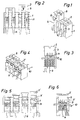
- the contact carrier 1 illustrated in FIGS. 1 to 3 generally forms a contact strip which has a transverse wire insertion slot 4 for each wire 10.
- the clamping cutting edge 5 of a protruding contact solder tab 6 projects transversely into each of these slots 4.
- Such a contact carrier 1 is seated on a printed circuit board (not shown in more detail), the contact solder lugs penetrating the printed circuit board and the back of which is soldered to the corresponding conductor tracks.
- such a contact carrier 1 has a corresponding number of depressible buttons 2, which have contact-side pressure deposits 3, which penetrate into the wire insertion slots 4 when the buttons 2 are pressed onto the contact carrier 1 and press the inserted wires into the clamping cutters 5 of the contact solder lugs 6.
- each key 2 has U-shaped pressure deposits 3 for the simultaneous connection of the clamping cutting edges 5 in two parallel wire insertion slots 4.
- each key 2 ' has a stamp-shaped pressure deposit 3' with an intermediate web 7 for the simultaneous connection of parallel clamping edges 5 in the wire insertion slot 4.
- each key has a groove-like depression 8 on the top side for attaching a screwdriver or the like for depressing the key.
- each button 2, 2 'on the contact carrier is advantageously releasably lockable both in an open position serving for pre-assembly and in its position causing contact.
- common raster means 9 are provided, as shown in FIGS. 1, 2 and 6 and others demonstrate.
- a contact carrier for the multiple wiring of printed circuit boards or the like thus results from the above, with means for solderless insulation displacement wire, in which the main problem of pressure on the wires resp. Cores for insulation displacement connection are optimally solved in spite of the tightest space, and are manufactured in the simplest way in terms of production and handling.
Abstract
Description
Die vorliegende Erfindung betrifft einen Kontakteträger für das Mehrfach-Beschalten von Printplatten o. dgl., mit Mitteln zur lötfreien Schneid-Klemm-Andrahtung.The present invention relates to a contact carrier for the multiple wiring of printed circuit boards or the like, with means for solderless insulation displacement connection.
In allen Bereichen der Schwachstromtechnik gewinnt die lötfreie Andrahtung erheblich an Bedeutung. In diesem Zusammenhang beschreibt die gleiche Anmelderin in ihrem CH-Patent 660'935 einen Stecker, insbesondere Rangierstecker, mit einem ansich bekannten Schneid-Klemm-Anschluss, welcher gestattet, einen Draht lötfrei am Anschluss zu fixieren, indem dieser Draht samt seiner Isolation in eine Kerbe eingedrückt wird, wobei die Kanten der Kerbe die Isolation durchschneiden und gering in das Leitermaterial unter Herstellung eines elektrischen Kontaktes eindringen.In all areas of low-voltage technology, solderless wiring is becoming increasingly important. In this context, the same applicant describes in her Swiss Patent 660,935 a plug, in particular a marshalling plug, with a known insulation displacement connection, which allows a wire to be fixed to the connection without soldering, by this wire and its insulation being inserted into one Notch is pushed in, the edges of the notch cutting through the insulation and making little in the conductor material of an electrical contact.
Diese lötfreie Schneid-Klemm-Andrahtung drängt sich auch bei modularen Steckverbindern für Telefon- oder Schwachstromanlagen auf, bei denen sich für den Drahtabstand bzw. Kontaktstiftabstand genormte oder doch normähnliche Raster herausgebildet haben, wobei dann für jeden Draht bzw. jede Ader ein länglicher Draht-Einlegeschlitz vorgesehen ist, der an einer Stelle von der querstehenden Klemmschneide der in der Regel senkrecht zum Einlegeschlitz abragenden Kontaktstifte durchsetzt ist.This solderless insulation displacement connection is also necessary for modular connectors for telephone or low-voltage systems, in which standardized or standard-like grids have developed for the wire spacing or contact pin spacing, with an elongated wire for each wire or wire. Insert slot is provided which is penetrated at one point by the transverse clamping cutting edge of the contact pins, which generally protrude perpendicularly to the insert slot.
Entsprechend betrifft das EP-Patent 310 832 der gleichen Anmelderin bereits einen Mehrfach-Kontaktstifthalter eines modularen Steckverbinders für Telefon- oder Schwachstromanlagen, mit Mitteln zur lötfreien Schneid-Klemm-Andrahtung, bei welchem die Mittel zur Schneid-Klemm-Andrahtung einen, auf den Körper des Kontaktstifthalters niederdrückbaren Schwenkdeckel umfassen, von welchem kontaktseitige Druckrippen abragen, die beim Niederdrücken des Deckels auf den Körper in dessen Draht-Einlegeschlitze eindringen und die eingelegten Drähte in die Klemmschneiden der Kontaktstifte pressen.Accordingly, EP patent 310 832 by the same applicant already relates to a multiple contact pin holder of a modular connector for telephone or low-voltage systems, with means for solderless insulation displacement connection, in which the insulation displacement connection means unites onto the body of the contact pin holder include swiveling cover, from which contact-side pressure ribs protrude, which penetrate into the wire insertion slots when the cover is pressed onto the body and press the inserted wires into the clamping cutters of the contact pins.
Für eine noch kompaktere Bauweise, wie dies für das Mehrfach-Beschalten von Printplatten erforderlich ist, ist aber eine Ausführung mit Schwenkdeckel nicht mehr anwendbar.For an even more compact design, such as this for multiple wiring of printed circuit boards is required, but a version with a swivel cover is no longer applicable.
Es ist deshalb Aufgabe der vorliegenden Erfindung, einen Kontakteträger für eine Mehrfach-Beschaltung von Printplatten zu schaffen, bei dem die lötfreie Schneid-Klemm-Andrahtung trotz geringster Abmessungen schnell, sicher und absolut problemlos erfolgen kann.It is therefore an object of the present invention to provide a contact carrier for multiple wiring of printed circuit boards, in which the solderless insulation displacement connection can be carried out quickly, safely and without any problems, despite the smallest dimensions.
Dies wird erfindungsgemäss dadurch erreicht, dass die Mittel zur Schneid-Klemm-Andrahtung mindestens eine, auf dem Kontakteträger niederdrückbare Taste umfassen, welche kontaktseitige Druckabragungen aufweist, die beim Niederdrücken der Taste auf den Kontakteträger in dessen Draht-Einlegeschlitze eindringen und die eingelegten Drähte in die Klemmschneiden der Kontaktlötfahnen oder -stifte pressen.This is achieved according to the invention in that the means for insulation displacement wiring comprise at least one button that can be pressed on the contact carrier, which has contact-side pressure deposits that penetrate into the wire insertion slots when the button is pressed on the contact carrier and the inserted wires into the Press clamping edges of the contact lugs or pins.
Durch diese Massnahmen ist das Problem der Druckausübung auf die Drähte resp. Adern trotz engster Platzverhältnisse umfänglich gelöst, wobei eine solche erfindungsgemässe Taste so breit gemacht werden kann, dass sich mehrere Drähte, beispielsweise vier, gleichzeitig in die Klemmschneiden der zugeordneten Kontaktlötfahnen eindrücken lassen.Through these measures, the problem of pressure on the wires resp. Wires extensively solved in spite of the tightest space, such a button according to the invention can be made so wide that several wires, for example four, can be pressed simultaneously into the clamping edges of the associated contact solder tags.
Vorzugsweise werden dabei die Tasten lösbar am Kontakteträger sowohl in einer der Vormontage dienenden Offenstellung als auch in ihrer Kontakt verursachenden Stellung verriegelbar.The buttons are preferably releasably lockable on the contact carrier both in an open position serving for pre-assembly and in their position causing contact.
Ferner bestehen vorteilhafte Ausgestaltungen dann, wenn die Taste U-förmige Druckabragungen aufweist für die gleichzeitige Beschaltung der Klemmschneiden in mindestens zwei Draht-Einlegeschlitzen; oder, wenn die Taste eine stempelförmige Druckabragung mit Zwischensteg aufweist für die gleichzeitige Beschaltung von parallelen Klemmschneiden im Draht-Einlegeschlitz.Furthermore, there are advantageous configurations when the button has U-shaped pressure deposits for the simultaneous connection of the clamping cutting edges in at least two wire insertion slots; or, if the button has a stamp-shaped pressure cut-off with an intermediate web for the simultaneous connection of parallel clamping edges in the wire insertion slot.
Für eine optimale Betätigung der Taste ist es zudem vorteilhaft, wenn die Taste obenseitig eine nutenartige Vertiefung zum Ansetzen eines Schraubenziehers oder dgl. zum Niederdrücken der Taste aufweist.For an optimal actuation of the button, it is also advantageous if the button has a groove-like depression on the top for attaching a screwdriver or the like for depressing the button.
Beispielsweise Ausführungsformen des Erfindungsgegenstandes sind nachfolgend anhand der Zeichnung näher erläutert.
Es zeigen:
- Fig. 1, 2 und 3
- eine erste Ausführungsform eines Kontakteträgers für Printplatte in einer schaubildartigen Darstellung, in Seitenansicht und in stirnseitiger Schnittansicht; und
- Fig. 4, 5 und 6
- eine weitere Ausführungsform eines Kontakteträgers in einer schaubildartigen Darstellung, in Seitenansicht und in stirnseitiger Schnittansicht.
Show it:
- 1, 2 and 3
- 1 shows a first embodiment of a contact carrier for printed circuit board in a diagram-like representation, in side view and in frontal sectional view; and
- 4, 5 and 6
- a further embodiment of a contact carrier in a diagrammatic representation, in side view and in a sectional end view.
Der in den Fig. 1 bis 3 veranschaulichte Kontaktträger 1 bildet in der Regel eine Kontaktleiste, welche für jeden Draht 10 einen querlaufenden Draht-Einlegeschlitz 4 aufweist. In jeden dieser Schlitze 4 ragt querstehend die Klemmschneide 5 einer abragenden Kontaktlötfahne 6 hinein.The
Ein solcher Kontakteträger 1 sitzt auf einer nicht näher gezeigten Printplatte auf, wobei die Kontaktlötfahnen die Printplatte durchdringen und deren Rückseite mit den entsprechenden Leiterbahnen verlötet sind.Such a
Erfindungsgemäss weist ein solcher Kontakteträger 1 eine entsprechende Anzahl niederdrückbare Tasten 2 auf, welche kontaktseitige Druckabragungen 3 aufweisen, die beim Niederdrücken der Tasten 2 auf den Kontakteträger 1 in dessen Draht-Einlegeschlitze 4 eindringen und die eingelegten Drähte in die Klemmschneiden 5 der Kontaktlötfahnen 6 pressen.According to the invention, such a
Bei der Ausgestaltung gemäss den Fig. 1 bis 3 weist jede Taste 2 U-förmige Druckabragungen 3 auf für die gleichzeitige Beschaltung der Klemmschneiden 5 in zwei parallelen Draht-Einlegeschlitzen 4.In the embodiment according to FIGS. 1 to 3, each
Bei der Ausführungsvariante gemäss den Fig. 4 bis 6 hingegen weist jede Taste 2' eine stempelförmige Druckabragung 3' mit Zwischensteg 7 auf für die gleichzeitige Beschaltung von parallelen Klemmschneiden 5 im Draht-Einlegeschlitz 4.In the embodiment variant according to FIGS. 4 to 6, on the other hand, each key 2 'has a stamp-shaped pressure deposit 3' with an
Für die Betätigung der Tasten 2,2' ist es von Vorteil, wenn jede Taste obenseitig eine nutenartige Vertiefung 8 zum Ansetzen eines Schraubenziehers oder dgl. zum Niederdrücken der Taste aufweist.For the actuation of the
Vorteilhaft ist ferner jede Taste 2,2' am Kontakteträger lösbar sowohl in einer der Vormontage dienenden Offenstellung als auch in ihrer Kontakt verursachenden Stellung verriegelbar.Furthermore, each
Hierfür sind übliche Rastermittel 9 vorgesehen, wie Fig. 1, 2 und 6 u.a. zeigen.For this purpose, common raster means 9 are provided, as shown in FIGS. 1, 2 and 6 and others demonstrate.
Aus dem Vorbeschriebenen ergibt sich somit ein Kontakteträger für das Mehrfach-Beschalten von Printplatten o. dgl., mit Mitteln zur lötfreien Schneid-Klemm-Andrahtung, bei dem das Hauptproblem der Druckausübung auf die Drähte resp. Adern zur Schneid-Klemm-Andrahtung trotz engster Raumverhältnisse optimal sowie herstellungs- und handhabungstechnisch auf einfachste Weise gelöst ist.A contact carrier for the multiple wiring of printed circuit boards or the like thus results from the above, with means for solderless insulation displacement wire, in which the main problem of pressure on the wires resp. Cores for insulation displacement connection are optimally solved in spite of the tightest space, and are manufactured in the simplest way in terms of production and handling.
Claims (5)
Applications Claiming Priority (2)
| Application Number | Priority Date | Filing Date | Title |
|---|---|---|---|
| CH02422/93A CH689132A5 (en) | 1993-08-16 | 1993-08-16 | Kontaktetraeger for the multi-Wiring of printed circuit boards. |
| CH2422/93 | 1993-08-16 |
Publications (2)
| Publication Number | Publication Date |
|---|---|
| EP0639870A2 true EP0639870A2 (en) | 1995-02-22 |
| EP0639870A3 EP0639870A3 (en) | 1995-05-10 |
Family
ID=4233445
Family Applications (1)
| Application Number | Title | Priority Date | Filing Date |
|---|---|---|---|
| EP94112695A Withdrawn EP0639870A3 (en) | 1993-08-16 | 1994-08-13 | Contact carrier for multiple wiring of printed boards or similar. |
Country Status (2)
| Country | Link |
|---|---|
| EP (1) | EP0639870A3 (en) |
| CH (1) | CH689132A5 (en) |
Cited By (2)
| Publication number | Priority date | Publication date | Assignee | Title |
|---|---|---|---|---|
| US5681182A (en) * | 1995-07-13 | 1997-10-28 | Reichle + De-Massari Ag | Modular contact mount for solderless insulation displacement wire connection of electrical wires |
| FR2768561A1 (en) * | 1997-09-17 | 1999-03-19 | Valeo Climatisation | Electrical wire connector |
Citations (2)
| Publication number | Priority date | Publication date | Assignee | Title |
|---|---|---|---|---|
| DE2014819A1 (en) * | 1970-03-26 | 1971-10-14 | Siemens Ag | Clamping element |
| DE2747395B1 (en) * | 1977-10-21 | 1979-04-26 | Siemens Ag | Device for solderless connection of a wire-shaped conductor |
-
1993
- 1993-08-16 CH CH02422/93A patent/CH689132A5/en not_active IP Right Cessation
-
1994
- 1994-08-13 EP EP94112695A patent/EP0639870A3/en not_active Withdrawn
Patent Citations (2)
| Publication number | Priority date | Publication date | Assignee | Title |
|---|---|---|---|---|
| DE2014819A1 (en) * | 1970-03-26 | 1971-10-14 | Siemens Ag | Clamping element |
| DE2747395B1 (en) * | 1977-10-21 | 1979-04-26 | Siemens Ag | Device for solderless connection of a wire-shaped conductor |
Cited By (2)
| Publication number | Priority date | Publication date | Assignee | Title |
|---|---|---|---|---|
| US5681182A (en) * | 1995-07-13 | 1997-10-28 | Reichle + De-Massari Ag | Modular contact mount for solderless insulation displacement wire connection of electrical wires |
| FR2768561A1 (en) * | 1997-09-17 | 1999-03-19 | Valeo Climatisation | Electrical wire connector |
Also Published As
| Publication number | Publication date |
|---|---|
| EP0639870A3 (en) | 1995-05-10 |
| CH689132A5 (en) | 1998-10-15 |
Similar Documents
| Publication | Publication Date | Title |
|---|---|---|
| EP1559175B1 (en) | Connector arrangement between a flexible ribbon cable and a component | |
| EP0730785B1 (en) | Terminal for electrical installations | |
| EP1207588B1 (en) | Electrical connector for flat cable or flexible printed circuit | |
| DE3541772A1 (en) | RECEIVING PART FOR ELECTRICAL CONNECTORS | |
| DE2054201B2 (en) | Electrical contact element intended for use in an electrical connector | |
| WO2008025180A2 (en) | Adapter and plug-in connection system | |
| EP0671780A1 (en) | Multiple contact and terminal block for communications equipment | |
| EP1507315B1 (en) | Bridge plug for electrical terminal blocks and the terminal block itself | |
| DE2443476A1 (en) | ELECTRICAL CONNECTOR | |
| DE2359425C3 (en) | Cable clamp and associated connection unit | |
| WO1997008785A1 (en) | Flat cable plug connecting device | |
| WO2009127315A1 (en) | Connection module | |
| DE19949387B4 (en) | Contact part for connection terminal | |
| EP0706235A2 (en) | Receptacle contact with latching means for an electrical connection | |
| DE3244470A1 (en) | ELECTRICAL CONNECTION SYSTEM AND CONNECTOR | |
| WO2002095877A1 (en) | Plug-in connector, especially for contacting an electric line with differently embodied contact points, and arrangement consisting of a plug-in connector and an electric line | |
| EP0856911A1 (en) | Multipole terminal block | |
| EP0310832B1 (en) | Multiple contact pin support for low-voltage installations | |
| EP0650217A1 (en) | Wire connecting device for low current installations | |
| DE2603151B2 (en) | Component for switching and / or isolating strips in distributors for telecommunications systems | |
| EP1154521B1 (en) | Connetor and mounting method of a connector | |
| EP0639870A2 (en) | Contact carrier for multiple wiring of printed boards or similar | |
| DE3543200A1 (en) | Flat-cable connector | |
| DE2517465B2 (en) | Connectors | |
| DE19964616B4 (en) | Connection terminal has insulating body in which contact element is mounted, and contact part inserted in mounting hole from inside, secured against inward movement by contact element |
Legal Events
| Date | Code | Title | Description |
|---|---|---|---|
| PUAI | Public reference made under article 153(3) epc to a published international application that has entered the european phase |
Free format text: ORIGINAL CODE: 0009012 |
|
| AK | Designated contracting states |
Kind code of ref document: A2 Designated state(s): DE FR GB IT |
|
| PUAL | Search report despatched |
Free format text: ORIGINAL CODE: 0009013 |
|
| AK | Designated contracting states |
Kind code of ref document: A3 Designated state(s): DE FR GB IT |
|
| 17P | Request for examination filed |
Effective date: 19951219 |
|
| 17Q | First examination report despatched |
Effective date: 19990125 |
|
| STAA | Information on the status of an ep patent application or granted ep patent |
Free format text: STATUS: THE APPLICATION IS DEEMED TO BE WITHDRAWN |
|
| 18D | Application deemed to be withdrawn |
Effective date: 19991228 |