EP0639294B1 - Semiconductor device with integrated rc network and schottky diode - Google Patents
Semiconductor device with integrated rc network and schottky diode Download PDFInfo
- Publication number
- EP0639294B1 EP0639294B1 EP94910817A EP94910817A EP0639294B1 EP 0639294 B1 EP0639294 B1 EP 0639294B1 EP 94910817 A EP94910817 A EP 94910817A EP 94910817 A EP94910817 A EP 94910817A EP 0639294 B1 EP0639294 B1 EP 0639294B1
- Authority
- EP
- European Patent Office
- Prior art keywords
- region
- conductive
- forming
- resistor
- capacitor
- Prior art date
- Legal status (The legal status is an assumption and is not a legal conclusion. Google has not performed a legal analysis and makes no representation as to the accuracy of the status listed.)
- Expired - Lifetime
Links
Images



Classifications
-
- H—ELECTRICITY
- H10—SEMICONDUCTOR DEVICES; ELECTRIC SOLID-STATE DEVICES NOT OTHERWISE PROVIDED FOR
- H10D—INORGANIC ELECTRIC SEMICONDUCTOR DEVICES
- H10D89/00—Aspects of integrated devices not covered by groups H10D84/00 - H10D88/00
- H10D89/60—Integrated devices comprising arrangements for electrical or thermal protection, e.g. protection circuits against electrostatic discharge [ESD]
- H10D89/601—Integrated devices comprising arrangements for electrical or thermal protection, e.g. protection circuits against electrostatic discharge [ESD] for devices having insulated gate electrodes, e.g. for IGFETs or IGBTs
-
- H—ELECTRICITY
- H10—SEMICONDUCTOR DEVICES; ELECTRIC SOLID-STATE DEVICES NOT OTHERWISE PROVIDED FOR
- H10D—INORGANIC ELECTRIC SEMICONDUCTOR DEVICES
- H10D89/00—Aspects of integrated devices not covered by groups H10D84/00 - H10D88/00
- H10D89/60—Integrated devices comprising arrangements for electrical or thermal protection, e.g. protection circuits against electrostatic discharge [ESD]
-
- H—ELECTRICITY
- H10—SEMICONDUCTOR DEVICES; ELECTRIC SOLID-STATE DEVICES NOT OTHERWISE PROVIDED FOR
- H10D—INORGANIC ELECTRIC SEMICONDUCTOR DEVICES
- H10D89/00—Aspects of integrated devices not covered by groups H10D84/00 - H10D88/00
- H10D89/60—Integrated devices comprising arrangements for electrical or thermal protection, e.g. protection circuits against electrostatic discharge [ESD]
- H10D89/601—Integrated devices comprising arrangements for electrical or thermal protection, e.g. protection circuits against electrostatic discharge [ESD] for devices having insulated gate electrodes, e.g. for IGFETs or IGBTs
- H10D89/711—Integrated devices comprising arrangements for electrical or thermal protection, e.g. protection circuits against electrostatic discharge [ESD] for devices having insulated gate electrodes, e.g. for IGFETs or IGBTs using bipolar transistors as protective elements
Definitions
- the present invention relates generally to integrated semiconductor devices.
- it relates to semiconductor devices having resistor and capacitor (RC) networks integrated with Schottky diodes on a single semiconductor substrate.
- RC resistor and capacitor
- RC networks and Schottky diodes have been used together in filter circuits.
- Such filter circuits are typically used to reduce electromagnetic and radio frequency interference (EMI/RFI) produced by computers and computer accessories.
- EMI/RFI electromagnetic and radio frequency interference
- Signals generally travel from one side of a transmission line to the other side. If the circuitry at the other end does not match the characteristic impedance of the transmission line, some of the signal amplitude can be reflected. This reflected signal can have the same or opposite polarity, depending on whether the mismatch is because of lower or higher impedance. As a result, signal ringing with undershoots or overshoots will occur. This signal ringing contributes to the radiation of EMI/RFI.
- Negative undershoots are more likely to occur than positive overshoots. This is due to the fact that, in semiconductor technology, n-channel MOS transistors and NPN bipolar transistors are faster, more powerful, and therefore more commonly used than p-channel MOS transistors and PNP bipolar transistors.
- Schottky diodes can be connected in parallel with a low pass RC filter.
- the cathode of the diode is connected to the transmission line and the anode is connected to ground.
- the Schottky diode is reverse biased and does not conduct current.
- negative undershoots exceeding the forward diode knee voltage are clamped and limited in amplitude.
- a Schottky diode is more effective than a regular junction diode at suppressing negative undershoots for two reasons. First, it has a lower knee voltage and therefore limits undershoots to a smaller amplitude. In other words, it suppresses ringing to a greater extent than does a junction diode. And second, unlike the junction diode, the Schottky diode has no carrier storage and therefore provides for a clean signal clipping of high frequency ringing.
- Schottky diodes have been used as collector-base clamping diodes in Schottky-TTL technology, to date, they have not been integrated with RC networks on a single integrated circuit chip. This stems from the difficulty in producing such a chip by combining the techniques used for forming RC networks with the techniques used for forming Schottky diodes.
- An integrated semiconductor device is defined in claim 1.
- a method of forming an integrated circuit according to claim 1 is defined in claim 9.
- a semiconductor device comprises a resistor, a capacitor, and a Schottky diode all formed on a single semiconductor substrate.
- the resistor and the capacitor are coupled together in series.
- the Schottky diode is coupled in parallel to this in series connection.
- the capacitor comprises a dielectric region sandwiched by two metal regions.
- the resistor comprises an N + -type well.
- the Schottky diode comprises an N-type tub, a metal region in contact with the tub, and an N + -type region formed in the N-type tub.
- the resistor and capacitor are coupled by a metal region which contacts one of the metal regions of the capacitor and the N + -type well of the resistor.
- the resistor and Schottky diode are coupled by a metal region which contacts the N + -type well of the resistor and the N + -type well of the Schottky diode.
- FIGS 1-5 illustrate a semiconductor device 10 in accordance with the present invention.
- like components are designated by like numerals.
- FIG. 1 provides a general circuit schematic of the semiconductor device 10.
- the Schottky diode 11 is coupled in parallel to resistor 12 and capacitor 13. Resistor 12 and capacitor 13 are coupled in series.
- the cathode 14 of Schottky diode 11 is coupled to the input terminal 15 and to the terminal 16 of resistor 12.
- the anode 17 of Schottky diode 12 is coupled to the ground terminal 18 and to the terminal 19 of capacitor 13.
- the terminal 20 of capacitor 13 is coupled to the terminal 21 of resistor 12.
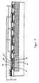
- Figure 2 provides a cross sectional layout of the preferred embodiment of the semiconductor device 10.
- the layout shows the Schottky diode 11, the resistor 12, and the capacitor 13 formed into a monolithic integrated circuit on a single semiconductor substrate 24.
- the following discussion details the processes, the materials, and the connections used in producing this layout.
- the substrate 24 is a P-type silicon material having a bulk resistivity of approximately 25-50 ohm cm.
- a lightly doped N-type tub 26 is then formed in the P-type substrate by implanting and/or diffusing a suitable impurity. In the preferred embodiment this impurity is phosphorous with a doping concentration of approximately 1 x 10 12 cm -3 .
- the N-tub 26 extends approximately 4 ⁇ m into the P-type substrate 24.
- a dielectric material is then selectively grown on the substrate 24 by conventional techniques for providing field isolation.
- this material is silicon dioxide and is grown to have a thickness of approximately 1.3 ⁇ m.
- the resulting field oxide regions 27-33 provide the field isolation.
- Heavily doped P + -type wells 34-37 and heavily doped N + -type wells 39-42 are then formed by conventional techniques used for implanting impurities.
- the P + -type wells 34-37 are formed by implanting boron into the N-type tub 26 with a doping concentration of approximately 1 x 10 14 cm -3 .
- the P + -type wells 34-37 extend approximately .5 ⁇ m into the N-type tub 26.
- the N + -type wells 39-42 are formed by implanting arsenic with a doping concentration of approximately 1 x 10 16 cm -3 .
- the N + -type wells 39-42 extend approximately .3 ⁇ m into the N-type tub 26.
- Another dielectric material such as silicon dioxide is then grown across the entire surface of the substrate 24. This layer is grown to have a thickness of approximately .2 ⁇ m. This layer is then selectively etched so that a first metal layer can be deposited onto selected areas of the N-type tub 26, the N + -type wells 39-42, and the P + -type wells 34-37. The remaining regions of this oxide layer are the oxide strips 45-57.
- the first metal layer is deposited across the entire surface.
- this metal layer is aluminum and is deposited with a thickness of approximately 1 ⁇ m. This first metal layer is then selectively etched to form the metal regions 61-67.
- this dielectric layer is silicon nitride and is deposited with a thickness of .2 ⁇ m. This dielectric layer is then selectively etched so that a second metal layer can be deposited onto the dielectric itself and onto the metal regions 61-67. The regions which remain are the dielectric regions 69-76.
- the second metal layer is deposited across the entire surface.
- this metal layer is also aluminum and is also deposited with a thickness of approximately 1 ⁇ m. This second metal layer is then selectively etched to form the metal regions 79-84.
- the resistor 12 primarily includes the N + -type well 39.
- This N + -type region has an area of approximately 30 ⁇ m by 30 ⁇ m and is in contact with the metal regions 62 and 63.
- the terminal 21 of resistor 12 is at the point where metal region 62 contacts the N + -type well 39.
- the terminal 16 of resistor 12 is at the point where metal region 63 contacts the N + -type well 39. Both contact points (i.e. terminals 16 and 21) are approximately 2.5 ⁇ m in width and approximately 20 ⁇ m apart from each other.
- the capacitor primarily includes the metal region 79, the dielectric region 69, and the metal region 61. Each of these regions has an area of approximately 350 ⁇ m by 350 ⁇ m.
- the terminal 19 of capacitor 13 is formed by the metal region 61 and is coupled to the ground terminal 18.
- the terminal 20 of capacitor 13 is formed by the metal region 79.
- the metal region 79 of capacitor 13 is coupled to the metal region 62. This is done with the via 78 of the metal region 79. Thus, the terminal 20 of capacitor 13 is coupled with the terminal 21 of resistor 12.
- the Schottky diode primarily includes the metal regions 64, 66, 81 and 83, the N-type tub 26, the P + -type wells 34-37, and the N + -type wells 40-42.
- the anode 17 of the Schottky diode is formed by the two parallel contact areas 86 and 87 where the metal regions 64 and 66 respectively contact the N-type tub 26.
- These parallel active areas 86 and 87 are approximately 8 ⁇ m in width and 320 ⁇ m in length. Thus, they form a set of inter-digitized Schottky contact fingers 86 and 87.
- the metal region 64 also contacts the P + -type wells 34 and 35 and the metal region 66 also contacts the P + -type wells 36 and 37.
- the resulting contact fingers 89-92 are each approximately 1 ⁇ m in width and 320 ⁇ m in length and are parallel to each other and to the active contact areas 86 and 87.
- the P + -type wells 34-37 are used to increase the reverse breakdown voltage of the Schottky diode 11.
- the P + -type wells 34 and 35 reduce the electric field between the N + -type wells 40 and 41 and the metal region 64.
- the P + -type wells 36 and 37 reduce the electric field between the N + -type wells 41 and 42 and the metal region 66.
- the paths for reverse breakdown between the metal region 64 and the N + -type wells 40 and 41 and the paths between the metal region 66 and the N + -type wells 41 and 42 are increased. Therefore, a greater reverse voltage is required for a reverse breakdown.
- Another advantage to the P + -type regions is that the forward knee voltage can be tailored to meet specific needs. This is done by increasing or decreasing the doping concentrations of the P + -type wells 34-37.
- the metal regions 81 and 83 are employed.
- the metal regions 81 and 83 therefore respectively serve as vias for coupling the parallel active contact areas 86 and 87 of the anode 17 to the ground terminal 18.
- the cathode 14 of the Schottky diode 11 is formed by the multiple contact areas 94-96 where the N + -type wells 40-42 contact the N-type tub 26.
- the resulting contact fingers 94-96 have each a width of approximately 4 ⁇ m and a length of approximately 320 ⁇ m and are parallel to each other and to the active area contact fingers 86 and 87.
- the N + -type wells 40-42 are used for contacting the N-type tub 26 because a direct metal contact to the N-type tub 26 would establish another Schottky contact area.
- the field oxide regions 29-33 together with the P + -type wells 34-37 provide separation between the active contact areas 86 and 87 and the N + -type wells 40-42.
- the field oxide regions 29-32 are each approximately 2 ⁇ m in width and 320 ⁇ m in length and are parallel to the active contact fingers 86 and 87.
- the P + -type wells 34-37 are each approximately 3 ⁇ m in width and 320 ⁇ m in length and are parallel to the active contact fingers 86 and 87 and the field oxide regions 29-32.
- the separation between each of the contact fingers 86 and 87 and one of the N + -type wells 40-42 is approximately 5 ⁇ m in width and 320 ⁇ m in length. In order to reduce the resistance between the active areas 86 and 87 and the N + -type wells 40-42, this separation could be made even smaller. However, this would have the undesirable effect of reducing the reverse breakdown voltage.
- the metal region 63 is used in order to couple the N + -type well 40 of the Schottky diode 11 to the N + -type well 39 of the resistor 12.
- the contact area at each of the N + -type wells 39 and 40 is approximately 2.5 ⁇ m in width.
- the metal region 63 couples the contact area 94 of cathode 14 with terminal 16 of the resistor 12.
- the metal region 80 is used to couple both the N + -type well 40 of the Schottky diode 11 and the N + -type well 39 of the resistor 12 to the input terminal 15.
- the metal region 80 therefore serves as a via for coupling the contact area 94 of cathode 14 to the input terminal 15.
- the metal regions 65, 67, 82, and 84 are used in order to couple the N + -type wells 41 and 42 of the Schottky diode 11 to the input terminal 15.
- the metal regions 65 and 67 respectively contact the N + -type wells 41 and 42 at the contact areas 95 and 96.
- the width of both of these contact areas is approximately 2.5 ⁇ m.
- the metal regions 82 and 84 respectively contact the metal regions 65 and 67 at a width of approximately 2.5 ⁇ m.
- the metal regions 82 and 84 serves as vias for coupling the contact areas 95 and 96 of cathode 14 with the input terminal 15.
- the field oxide region 28 provides separation between the N-type tub 26 and the N + -type well 39 and between the N + -type well 40 and the N + -type well 39. Since the field oxide region 28 is approximately 5.5 ⁇ m in width, the separation between the two N + -type wells 39 and 40 is approximately this same width. Furthermore, the separation between the N + -type well 39 and the N-type tub 26 is approximately 3.5 ⁇ m.
- the Schottky diode 11 can be configured to draw more current. This is done by making the width of the active contact areas 86 and 87 larger. However, as this width is increased, the associated capacitance at the active contact area is also increased.
- additional parallel Schottky contact fingers can be constructed in the same manner as the contact finger 87. This also requires constructing associated additional N + -type to N-type contact fingers in the same manner as the contact fingers 95 and 96.
- the metal regions 79-84 contact the metal regions 61-67 respectively.
- the metal regions 79-84 do not directly contact the N + -type wells, P + -type wells 34-37, or the N-type tub 26. If this were attempted, undesirable inaccuracies would result from having to etch through both the silicon nitride layer and the second silicon dioxide layer deposited during fabrication.
- FIG. 3 provides an alternative embodiment of the semiconductor device 10.
- the Schottky diode 11 only has a single Schottky active contact area 86 rather than the set of inter-digitized Schottky contact areas 86 and 87 of Figure 2.
- the single active contact area 86 is circular shaped.
- the metal regions 64 and 81 are circular shaped as well.
- the N + -type well 40, the field oxide region 29, the oxide strips 48-50, and the P + -type 34 region are all ring shaped.
- the N + -type to N-type contact area 94 is ring shaped as well.
- the metal region 63 has a ring shaped portion 97 which contacts the ring shaped N + -type well 40.
- the metal region 81 has a ring shaped portion 98 which contacts the ring shaped portion of the metal region 63.
- the same type of process is used in fabricating this embodiment as was described earlier for the embodiment in Figure 2.
- Figure 4 provides another embodiment of the semiconductor device 10.
- the resistor includes a second N-type tub 25 formed in the P-type substrate 24. And, in the N-type tub 25, there is formed a P + -type well 99.
- the metal regions 62 and 63 both contact the P + -type well 99. These contacts form the two terminals 21 and 16 of the resistor 12. Otherwise, the connections and the components are the same as in the earlier described embodiment in Figure 2.
- the second N-type tub 25 is formed at the same time using the same processes and materials as was described earlier for the N-type tube 26. Furthermore, the P + -type well 99 is formed at the same time using the same processes and materials as was described earlier for the P + -type wells 34-37. Otherwise, the fabrication process is the same as that described earlier for the embodiment in Figure 2.
- Figure 5 shows still another embodiment of semiconductor device 11.
- the resistor 12 includes the thin film resistive material 23 deposited on the field oxide region 27.
- the metal regions 62 and 63 both contact the thin film material 23. These contacts form the two terminals 21 and 16 of the resistor 12. Otherwise, the connections and the components are the same as in the earlier described embodiment in Figure 2.
- the thin film material 23 is deposited onto the field oxide region 27 after the field oxide regions 27 and 29-32 have been formed and after the oxide strips 45 and 47 have been formed.
- this film material comprises tantalum and is deposited with a thickness of approximately 1 ⁇ m. Then, the first metal layer is deposited and the metal regions 61-67 are formed. Otherwise, the fabrication process is the same as that described earlier for the embodiment in Figure 2.
Landscapes
- Electrodes Of Semiconductors (AREA)
- Semiconductor Integrated Circuits (AREA)
Abstract
Description
- The present invention relates generally to integrated semiconductor devices. In particular, it relates to semiconductor devices having resistor and capacitor (RC) networks integrated with Schottky diodes on a single semiconductor substrate.
- In the past, RC networks and Schottky diodes have been used together in filter circuits. Such filter circuits are typically used to reduce electromagnetic and radio frequency interference (EMI/RFI) produced by computers and computer accessories.
- These computers and accessories are routinely operated only a short distance away from telecommunication equipment. For example, a personal computer is often operated in close proximity to a television set and computers in police cars are operated side by side with police communication gear. Many of these computers have high clock rates and digital signals whose rise and fall times are extremely short. In addition, many computer accessories operate at similarly high speeds. For example, memory cards, video accelerator cards, modems, fax boards, co-processor cards, and data compression hardware all operate at very high frequencies. As a result, the high speed data lines in these computers and accessories produce EMI/RFI.
- Without additional counter measures, these popular and widespread computers and accessories would contaminate the air waves and interfere with communication equipment. For example, cordless telephones, cellular telephones, radios, televisions, and burglar alarms could all be affected. Furthermore, important non-communication equipment, like pacemakers or other medical equipment, could also be impacted.
- Therefore, it is desirable to have counter measures which suppress the EMI/RFI produced by the high speed data lines in computers and computer accessories. However, it is also desirable that such counter measures are inexpensive, occupy little space, ensure proper testing, and produce only small delays.
- In the past, several techniques have been used for shielding high speed data lines. However, these methods have not proven to be effective at optimizing cost, size, ease of testing, minimization of delays, and suppression of EMI/RFI.
- One method has utilized metallic shielding with feed through capacitors coupled to the high speed data lines. However, this method is expensive. Furthermore, it is no longer feasible in light of the need for portable computers and computer accessories and the availability of light weight plastic enclosures.
- Another method has been to simply use low pass integrated RC filters produced by thin film techniques. The use of a resistor in series with a capacitor limits the maximum attenuation at higher frequencies to a constant value. However, such filters do not effectively suppress EMF/RFI produced by signal ringing on a transmission line.
- Signals generally travel from one side of a transmission line to the other side. If the circuitry at the other end does not match the characteristic impedance of the transmission line, some of the signal amplitude can be reflected. This reflected signal can have the same or opposite polarity, depending on whether the mismatch is because of lower or higher impedance. As a result, signal ringing with undershoots or overshoots will occur. This signal ringing contributes to the radiation of EMI/RFI.
- Negative undershoots are more likely to occur than positive overshoots. This is due to the fact that, in semiconductor technology, n-channel MOS transistors and NPN bipolar transistors are faster, more powerful, and therefore more commonly used than p-channel MOS transistors and PNP bipolar transistors.
- To suppress signal ringing with undershoots, Schottky diodes can be connected in parallel with a low pass RC filter. The cathode of the diode is connected to the transmission line and the anode is connected to ground. For normal signal levels on the transmission line, the Schottky diode is reverse biased and does not conduct current. However, negative undershoots exceeding the forward diode knee voltage are clamped and limited in amplitude.
- A Schottky diode is more effective than a regular junction diode at suppressing negative undershoots for two reasons. First, it has a lower knee voltage and therefore limits undershoots to a smaller amplitude. In other words, it suppresses ringing to a greater extent than does a junction diode. And second, unlike the junction diode, the Schottky diode has no carrier storage and therefore provides for a clean signal clipping of high frequency ringing.
- In the past, Schottky diodes have only been used as discrete circuit elements in these filter circuits. Because of this, these filter circuits are costly to produce, occupy a great deal of space, require extra connections for testing, and have significant delays due to large spacing between elements.
- Although Schottky diodes have been used as collector-base clamping diodes in Schottky-TTL technology, to date, they have not been integrated with RC networks on a single integrated circuit chip. This stems from the difficulty in producing such a chip by combining the techniques used for forming RC networks with the techniques used for forming Schottky diodes.
- Document "ESSDERC '92-1992 22nd European Solid State Device Research Conference, Leuven, Belgium, 14-17 Sept. 1992, Vol. 19, no. 1-4, pages 413-416 discloses an RC circuit with a thin film resistor.
- An integrated semiconductor device according to the present invention is defined in claim 1. A method of forming an integrated circuit according to claim 1 is defined in claim 9.
- In an embodiment of the invention a semiconductor device comprises a resistor, a capacitor, and a Schottky diode all formed on a single semiconductor substrate. The resistor and the capacitor are coupled together in series. The Schottky diode is coupled in parallel to this in series connection.
- The capacitor comprises a dielectric region sandwiched by two metal regions. The resistor comprises an N+-type well. The Schottky diode comprises an N-type tub, a metal region in contact with the tub, and an N+-type region formed in the N-type tub.
- The resistor and capacitor are coupled by a metal region which contacts one of the metal regions of the capacitor and the N+-type well of the resistor. The resistor and Schottky diode are coupled by a metal region which contacts the N+-type well of the resistor and the N+-type well of the Schottky diode.
- The foregoing and other objects of the invention will become apparent in reading the following detailed description and in reference to the following drawings, in which:
- Figure 1 shows a general circuit schematic of the present invention;
- Figure 2 shows a layout of the present invention employing inter-digitized Schottky contact area;
- Figure 3 shows a layout of the present invention employing a single circular Schottky contact finger;
- Figure 4 shows a layout of the present invention employing a resistor comprising a P+-type well formed in an N-type tub;
- Figure 5 shows a layout of the present invention employing a resistor comprising a thin film material.
-
- Figures 1-5 illustrate a
semiconductor device 10 in accordance with the present invention. In these figures, like components are designated by like numerals. - Figure 1 provides a general circuit schematic of the
semiconductor device 10. TheSchottky diode 11 is coupled in parallel toresistor 12 andcapacitor 13.Resistor 12 andcapacitor 13 are coupled in series. - The
cathode 14 ofSchottky diode 11 is coupled to theinput terminal 15 and to theterminal 16 ofresistor 12. Theanode 17 ofSchottky diode 12 is coupled to theground terminal 18 and to theterminal 19 ofcapacitor 13. The terminal 20 ofcapacitor 13 is coupled to theterminal 21 ofresistor 12. - Figure 2 provides a cross sectional layout of the preferred embodiment of the
semiconductor device 10. The layout shows theSchottky diode 11, theresistor 12, and thecapacitor 13 formed into a monolithic integrated circuit on asingle semiconductor substrate 24. The following discussion details the processes, the materials, and the connections used in producing this layout. - The
substrate 24 is a P-type silicon material having a bulk resistivity of approximately 25-50 ohm cm. A lightly doped N-type tub 26 is then formed in the P-type substrate by implanting and/or diffusing a suitable impurity. In the preferred embodiment this impurity is phosphorous with a doping concentration of approximately 1 x 1012 cm-3. The N-tub 26 extends approximately 4 µm into the P-type substrate 24. - A dielectric material is then selectively grown on the
substrate 24 by conventional techniques for providing field isolation. In the preferred embodiment this material is silicon dioxide and is grown to have a thickness of approximately 1.3 µm. The resulting field oxide regions 27-33 provide the field isolation. - Heavily doped P+-type wells 34-37 and heavily doped N+-type wells 39-42 are then formed by conventional techniques used for implanting impurities. In the preferred embodiment, the P+-type wells 34-37 are formed by implanting boron into the N-
type tub 26 with a doping concentration of approximately 1 x 1014 cm-3. The P+-type wells 34-37 extend approximately .5 µm into the N-type tub 26. Also, in the preferred embodiment, the N+-type wells 39-42 are formed by implanting arsenic with a doping concentration of approximately 1 x 1016 cm-3. The N+-type wells 39-42 extend approximately .3 µm into the N-type tub 26. - Another dielectric material such as silicon dioxide is then grown across the entire surface of the
substrate 24. This layer is grown to have a thickness of approximately .2 µm. This layer is then selectively etched so that a first metal layer can be deposited onto selected areas of the N-type tub 26, the N+-type wells 39-42, and the P+-type wells 34-37. The remaining regions of this oxide layer are the oxide strips 45-57. - After the second oxide layer is etched, the first metal layer is deposited across the entire surface. In the preferred embodiment, this metal layer is aluminum and is deposited with a thickness of approximately 1 µm. This first metal layer is then selectively etched to form the metal regions 61-67.
- A suitable dielectric material is then deposited across the entire surface. In the preferred embodiment, this dielectric layer is silicon nitride and is deposited with a thickness of .2 µm. This dielectric layer is then selectively etched so that a second metal layer can be deposited onto the dielectric itself and onto the metal regions 61-67. The regions which remain are the dielectric regions 69-76.
- After the dielectric layer is etched, the second metal layer is deposited across the entire surface. In the preferred embodiment, this metal layer is also aluminum and is also deposited with a thickness of approximately 1 µm. This second metal layer is then selectively etched to form the metal regions 79-84.
- The
resistor 12 primarily includes the N+-type well 39. This N+-type region has an area of approximately 30 µm by 30 µm and is in contact with themetal regions resistor 12 is at the point wheremetal region 62 contacts the N+-type well 39. The terminal 16 ofresistor 12 is at the point wheremetal region 63 contacts the N+-type well 39. Both contact points (i.e.terminals 16 and 21) are approximately 2.5 µm in width and approximately 20 µm apart from each other. - The capacitor primarily includes the metal region 79, the
dielectric region 69, and the metal region 61. Each of these regions has an area of approximately 350 µm by 350 µm. The terminal 19 ofcapacitor 13 is formed by the metal region 61 and is coupled to theground terminal 18. The terminal 20 ofcapacitor 13 is formed by the metal region 79. - The metal region 79 of
capacitor 13 is coupled to themetal region 62. This is done with the via 78 of the metal region 79. Thus, theterminal 20 ofcapacitor 13 is coupled with the terminal 21 ofresistor 12. - The Schottky diode primarily includes the
metal regions 64, 66, 81 and 83, the N-type tub 26, the P+-type wells 34-37, and the N+-type wells 40-42. - The
anode 17 of the Schottky diode is formed by the two parallel contact areas 86 and 87 where the metal regions 64 and 66 respectively contact the N-type tub 26. These parallel active areas 86 and 87 are approximately 8 µm in width and 320 µm in length. Thus, they form a set of inter-digitized Schottky contact fingers 86 and 87. - The metal region 64 also contacts the P+-
type wells type wells - The P+-type wells 34-37 are used to increase the reverse breakdown voltage of the
Schottky diode 11. The P+-type wells type wells type wells type wells type wells type wells - Another advantage to the P+-type regions is that the forward knee voltage can be tailored to meet specific needs. This is done by increasing or decreasing the doping concentrations of the P+-type wells 34-37.
- In order to couple the metal regions 64 and 66 of the
Schottky diode 11 to theground terminal 18, themetal regions 81 and 83 are employed. Themetal regions 81 and 83 therefore respectively serve as vias for coupling the parallel active contact areas 86 and 87 of theanode 17 to theground terminal 18. - The
cathode 14 of theSchottky diode 11 is formed by the multiple contact areas 94-96 where the N+-type wells 40-42 contact the N-type tub 26. The resulting contact fingers 94-96 have each a width of approximately 4 µm and a length of approximately 320 µm and are parallel to each other and to the active area contact fingers 86 and 87. The N+-type wells 40-42 are used for contacting the N-type tub 26 because a direct metal contact to the N-type tub 26 would establish another Schottky contact area. - The field oxide regions 29-33 together with the P+-type wells 34-37 provide separation between the active contact areas 86 and 87 and the N+-type wells 40-42. The field oxide regions 29-32 are each approximately 2 µm in width and 320 µm in length and are parallel to the active contact fingers 86 and 87. The P+-type wells 34-37 are each approximately 3 µm in width and 320 µm in length and are parallel to the active contact fingers 86 and 87 and the field oxide regions 29-32. Thus, the separation between each of the contact fingers 86 and 87 and one of the N+-type wells 40-42 is approximately 5 µm in width and 320 µm in length. In order to reduce the resistance between the active areas 86 and 87 and the N+-type wells 40-42, this separation could be made even smaller. However, this would have the undesirable effect of reducing the reverse breakdown voltage.
- The
metal region 63 is used in order to couple the N+-type well 40 of theSchottky diode 11 to the N+-type well 39 of theresistor 12. The contact area at each of the N+-type wells 39 and 40 is approximately 2.5 µm in width. Thus, themetal region 63 couples thecontact area 94 ofcathode 14 withterminal 16 of theresistor 12. - Furthermore, the metal region 80 is used to couple both the N+-type well 40 of the
Schottky diode 11 and the N+-type well 39 of theresistor 12 to theinput terminal 15. The metal region 80 therefore serves as a via for coupling thecontact area 94 ofcathode 14 to theinput terminal 15. - The
metal regions 65, 67, 82, and 84 are used in order to couple the N+-type wells Schottky diode 11 to theinput terminal 15. Themetal regions 65 and 67 respectively contact the N+-type wells contact areas 95 and 96. The width of both of these contact areas is approximately 2.5 µm. Furthermore, the metal regions 82 and 84 respectively contact themetal regions 65 and 67 at a width of approximately 2.5 µm. Thus, the metal regions 82 and 84 serves as vias for coupling thecontact areas 95 and 96 ofcathode 14 with theinput terminal 15. - The
field oxide region 28 provides separation between the N-type tub 26 and the N+-type well 39 and between the N+-type well 40 and the N+-type well 39. Since thefield oxide region 28 is approximately 5.5 µm in width, the separation between the two N+-type wells 39 and 40 is approximately this same width. Furthermore, the separation between the N+-type well 39 and the N-type tub 26 is approximately 3.5 µm. - The
Schottky diode 11 can be configured to draw more current. This is done by making the width of the active contact areas 86 and 87 larger. However, as this width is increased, the associated capacitance at the active contact area is also increased. - In order to remedy such a problem and still provide the
Schottky diode 11 with the capability to draw more current, additional parallel Schottky contact fingers can be constructed in the same manner as the contact finger 87. This also requires constructing associated additional N+-type to N-type contact fingers in the same manner as thecontact fingers 95 and 96. - As is shown in Figure 2, the metal regions 79-84 contact the metal regions 61-67 respectively. The metal regions 79-84 do not directly contact the N+-type wells, P+-type wells 34-37, or the N-
type tub 26. If this were attempted, undesirable inaccuracies would result from having to etch through both the silicon nitride layer and the second silicon dioxide layer deposited during fabrication. - Figure 3 provides an alternative embodiment of the
semiconductor device 10. In this embodiment, theSchottky diode 11 only has a single Schottky active contact area 86 rather than the set of inter-digitized Schottky contact areas 86 and 87 of Figure 2. - The single active contact area 86 is circular shaped. Thus, the
metal regions 64 and 81 are circular shaped as well. Furthermore, the N+-type well 40, thefield oxide region 29, the oxide strips 48-50, and the P+-type 34 region are all ring shaped. Thus, the N+-type to N-type contact area 94 is ring shaped as well. In addition, themetal region 63 has a ring shaped portion 97 which contacts the ring shaped N+-type well 40. And, themetal region 81 has a ring shaped portion 98 which contacts the ring shaped portion of themetal region 63. The same type of process is used in fabricating this embodiment as was described earlier for the embodiment in Figure 2. - Figure 4 provides another embodiment of the
semiconductor device 10. In this embodiment, the resistor includes a second N-type tub 25 formed in the P-type substrate 24. And, in the N-type tub 25, there is formed a P+-type well 99. Themetal regions type well 99. These contacts form the twoterminals resistor 12. Otherwise, the connections and the components are the same as in the earlier described embodiment in Figure 2. - In this embodiment, the second N-
type tub 25 is formed at the same time using the same processes and materials as was described earlier for the N-type tube 26. Furthermore, the P+-type well 99 is formed at the same time using the same processes and materials as was described earlier for the P+-type wells 34-37. Otherwise, the fabrication process is the same as that described earlier for the embodiment in Figure 2. - Figure 5 shows still another embodiment of
semiconductor device 11. In this embodiment, theresistor 12 includes the thin filmresistive material 23 deposited on thefield oxide region 27. Themetal regions thin film material 23. These contacts form the twoterminals resistor 12. Otherwise, the connections and the components are the same as in the earlier described embodiment in Figure 2. - In this embodiment, the
thin film material 23 is deposited onto thefield oxide region 27 after thefield oxide regions 27 and 29-32 have been formed and after the oxide strips 45 and 47 have been formed. In the preferred embodiment this film material comprises tantalum and is deposited with a thickness of approximately 1 µm. Then, the first metal layer is deposited and the metal regions 61-67 are formed. Otherwise, the fabrication process is the same as that described earlier for the embodiment in Figure 2. - While the present invention has been described with reference to a few specific embodiments, the description is illustrative of the invention and is not to be construed as limiting the invention. Various modifications may occur to those skilled in the art without departing from the true spirit and scope of the invention as defined by the appended claims.
Claims (16)
- An integrated semiconductor device comprising:a substrate (24);a resistive region of a resistor formed of a doped well (39) or a single thin film (23);first and second conductive regions (62, 63) to define first and second terminals (21, 16) of the resistor (12);a third conductive region (61) defining a first plate of a capacitor (13);a dielectric region (69) extending above the third conductive region (61) and defining a dielectric portion of the capacitor (13); anda fourth conductive region (79) having a first portion extending above the dielectric region (69) and a second portion in contact with the first conductive region (62), the first portion defining a second plate of the capacitor (13) and the second portion coupling the second plate of the capacitor (13) to the first terminal (21) of the resistor (12);wherein the first, second, and third conductive regions (62, 63, 61) are formed from a first conductive layer formed above the substrate (24) and the fourth conductive region (79) is formed from a second conductive layer formed above the first conductive layer;wherein the first and second conductive regions (62, 63) are in direct contact with the resistive region; andthe second portion of the fourth conductive region (79) extends above part of the resistive region, where it contacts the first conductive region (62).
- The integrated semiconductor device of claim 1:
wherein the single thin film (23) is formed on a field oxide region (27) above the substrate (24). - The integrated semiconductor device of claim 1 wherein the doped well (39) is formed in the substrate (24).
- The integrated semiconductor device of claim 1: comprising a doped tub (25) formed in the substrate (24);
wherein the doped well (99) is formed in and oppositely doped to the doped tub (25). - The integrated semiconductor device of one of the claims 1 to 4 wherein the first, second, third, and fourth conductive regions (62, 63, 64, 79) comprise metal.
- The integrated semiconductor device of one of the claims 1 to 5 further comprising:a lightly doped tub (26) formed in the substrate (24);a first heavily doped well (40) formed in the lightly doped tub so as to define the cathode (14) of a Schottky diode (11);a fifth conductive region (64) in contact with and extending over a portion of the lightly doped tub (26) so as to define the anode (17) of the Schottky diode (11);wherein the second conductive region (63) is also in contact with the first heavily doped well (40) so as to couple the second terminal (16) of the resistor (12) to the cathode (14) of the Schottky diode (11).
- The integrated semiconductor device of claim 6 wherein the fifth conductive region (64) is formed from the first conductive layer.
- The integrated semiconductor device of claim 6 or 7 wherein the first, second, third, fourth, and fifth conductive regions (62, 63, 61, 64, 79) comprise metal.
- A method of forming an integrated semiconductor according to claim 1 comprising the steps of:forming the resistive region;forming a first conductive layer above the substrate (24);from the first conductive layer, forming first and second conductive regions (62, 63) to define first and second terminals (21,16) of a resistor (12) and forming a third conductive region (61) to define a first plate of a capacitor (13);forming a dielectric region (69) extending above the third conductive region (61) and defining a dielectric portion of the capacitor (13); andforming a second conductive layer formed above the first conductive layer;from the second conductive layer, forming a fourth conductive region (79) having a first portion extending above the dielectric region (69) and a second portion in contact with the first conductive region (62), the first portion defining a second plate of the capacitor (13) and the second portion coupling the second plate of the capacitor (13) to the first terminal (21) of the resistor (12);wherein the first and second conductive regions (62, 63) are formed to be in direct contact with the resistive region; andthe second portion of the fourth conductive region (79) extends above part of the resistive region, where it contacts the first conductive region (62).
- The method of claim 9 further comprising the step of:forming a field oxide region (27) above the substrate (24)wherein the step of forming the resistive region comprises forming the single thin film (23) on the field oxide region (27).
- The method of claim 9 wherein the step of forming the resistive region comprises forming the doped well (39) in the substrate (24).
- The method of claim 9 further comprising the step of:forming a doped tub (25) in the substrate (24);wherein the doped well (99) is formed in and oppositely doped to the doped tub (25).
- The method of one of the claims 9 to 12 wherein metal is used for the first, second, third, and fourth conductive regions (62, 63, 64, 79).
- The method of one of the claims 9 to 13 further comprising the steps of:forming a lightly doped tub (26) in the substrate (24);forming a first heavily doped well (40) in the lightly doped tub so as to define the cathode (14) of a Schottky diode (11);forming a fifth conductive region (64) in contact with and extending over a portion of the lightly doped tub (26) so as to define the anode (17) of the Schottky diode (11);wherein the second conductive region (63) is also in contact with the first heavily doped well (40) so as to couple the second terminal (16) of the resistor (12) to the cathode (14) of the Schottky diode (11).
- The method of claim 14 wherein the fifth conductive region (64) is formed from the first conductive layer.
- The method of claim 14 or 15 wherein metal is used for the first, second, third, fourth, and fifth conductive regions.
Applications Claiming Priority (3)
| Application Number | Priority Date | Filing Date | Title |
|---|---|---|---|
| US25600 | 1993-03-03 | ||
| US08/025,600 US5355014A (en) | 1993-03-03 | 1993-03-03 | Semiconductor device with integrated RC network and Schottky diode |
| PCT/US1994/002287 WO1994020988A1 (en) | 1993-03-03 | 1994-03-03 | Semiconductor device with integrated rc network and schottky diode |
Publications (3)
| Publication Number | Publication Date |
|---|---|
| EP0639294A1 EP0639294A1 (en) | 1995-02-22 |
| EP0639294A4 EP0639294A4 (en) | 1995-06-14 |
| EP0639294B1 true EP0639294B1 (en) | 2001-08-08 |
Family
ID=21826996
Family Applications (1)
| Application Number | Title | Priority Date | Filing Date |
|---|---|---|---|
| EP94910817A Expired - Lifetime EP0639294B1 (en) | 1993-03-03 | 1994-03-03 | Semiconductor device with integrated rc network and schottky diode |
Country Status (5)
| Country | Link |
|---|---|
| US (1) | US5355014A (en) |
| EP (1) | EP0639294B1 (en) |
| JP (1) | JP2711023B2 (en) |
| DE (1) | DE69427889T2 (en) |
| WO (1) | WO1994020988A1 (en) |
Families Citing this family (22)
| Publication number | Priority date | Publication date | Assignee | Title |
|---|---|---|---|---|
| JP2822943B2 (en) * | 1995-06-30 | 1998-11-11 | 日本電気株式会社 | Frequency correction circuit |
| US5652460A (en) * | 1995-10-06 | 1997-07-29 | California Micro Devices Corporation | Integrated resistor networks having reduced cross talk |
| US5706163A (en) * | 1995-11-28 | 1998-01-06 | California Micro Devices Corporation | ESD-protected thin film capacitor structures |
| US5760662A (en) * | 1996-02-28 | 1998-06-02 | California Micro Devices Corporation | Methods and apparatus for improving frequency response of integrated RC filters with additional ground pins |
| US5716880A (en) * | 1997-02-20 | 1998-02-10 | Chartered Semiconductor Manufacturing Pte Ltd. | Method for forming vertical polysilicon diode compatible with CMOS/BICMOS formation |
| GB9706154D0 (en) * | 1997-03-25 | 1997-05-14 | Philips Electronics Nv | Circuit simulator |
| US6342681B1 (en) | 1997-10-15 | 2002-01-29 | Avx Corporation | Surface mount coupler device |
| JP3278765B2 (en) * | 1997-11-17 | 2002-04-30 | 日本電気株式会社 | Negative voltage generation circuit |
| US6229181B1 (en) | 1999-04-30 | 2001-05-08 | Digital Devices, Inc. | Semiconductor device and method of forming a semiconductor structure to provide electrostatic discharge protection |
| US6262442B1 (en) * | 1999-04-30 | 2001-07-17 | Dmitri G. Kravtchenko | Zener diode and RC network combination semiconductor device for use in integrated circuits |
| TW428306B (en) * | 1999-07-01 | 2001-04-01 | Viking Tech Corp | Packaging method for thin-film passive device on silicon |
| US7019377B2 (en) * | 2002-12-17 | 2006-03-28 | Micrel, Inc. | Integrated circuit including high voltage devices and low voltage devices |
| US6798641B1 (en) * | 2003-08-25 | 2004-09-28 | National Semiconductor Corporation | Low cost, high density diffusion diode-capacitor |
| KR100689884B1 (en) * | 2005-02-15 | 2007-03-09 | 삼성전자주식회사 | Semiconductor device for noise reduction using Schottky diode and manufacturing method thereof |
| KR101320516B1 (en) * | 2007-07-20 | 2013-10-22 | 삼성전자주식회사 | Semiconductor device having electrostatic discharge protection circuit and method of manufacturing the same |
| US7851881B1 (en) * | 2008-03-21 | 2010-12-14 | Microsemi Corporation | Schottky barrier diode (SBD) and its off-shoot merged PN/Schottky diode or junction barrier Schottky (JBS) diode |
| JP5678407B2 (en) * | 2009-03-02 | 2015-03-04 | 日産自動車株式会社 | Semiconductor device |
| JP5453848B2 (en) * | 2009-03-05 | 2014-03-26 | 日産自動車株式会社 | Semiconductor device and power conversion device |
| US9214457B2 (en) | 2011-09-20 | 2015-12-15 | Alpha & Omega Semiconductor Incorporated | Method of integrating high voltage devices |
| JP6389300B2 (en) * | 2011-10-17 | 2018-09-12 | ローム株式会社 | Semiconductor device |
| JP6176817B2 (en) | 2011-10-17 | 2017-08-09 | ローム株式会社 | Chip diode and diode package |
| US8963277B2 (en) | 2013-03-13 | 2015-02-24 | Macronix International Co., Ltd. | Semiconductor structure and method of manufacturing the same |
Family Cites Families (10)
| Publication number | Priority date | Publication date | Assignee | Title |
|---|---|---|---|---|
| DE2733615A1 (en) * | 1977-07-26 | 1979-02-01 | Ibm Deutschland | Integrated semiconductor with diode-resistor configuration - has pinch resistor with pinch doped region greater than cross=section of residual resistor doped region |
| JPS58147145A (en) * | 1982-02-26 | 1983-09-01 | Sony Corp | Manufacture of semiconductor device |
| JPS61141167A (en) * | 1984-12-13 | 1986-06-28 | Nippon Precision Saakitsutsu Kk | Manufacture of semiconductor device |
| JPS6292459A (en) * | 1985-10-18 | 1987-04-27 | Sanyo Electric Co Ltd | semiconductor capacitive coupling element |
| JPS63133660A (en) * | 1986-11-26 | 1988-06-06 | Sony Corp | Semiconductor device |
| JPH02159756A (en) * | 1988-12-14 | 1990-06-19 | Nec Corp | Thin film resistance element of tantalum |
| US5047826A (en) * | 1989-06-30 | 1991-09-10 | Texas Instruments Incorporated | Gigaohm load resistor for BICMOS process |
| EP0453785A1 (en) * | 1990-04-24 | 1991-10-30 | Oerlikon Contraves AG | Method of making multilayer thin film circuit comprising integrated thin film resistors |
| JPH04306715A (en) * | 1991-04-03 | 1992-10-29 | Sharp Corp | Stabilized power source circuit |
| US5218222A (en) * | 1992-09-16 | 1993-06-08 | Micron Semiconductor, Inc. | Output ESD protection circuit |
-
1993
- 1993-03-03 US US08/025,600 patent/US5355014A/en not_active Expired - Lifetime
-
1994
- 1994-03-03 JP JP6520150A patent/JP2711023B2/en not_active Expired - Lifetime
- 1994-03-03 WO PCT/US1994/002287 patent/WO1994020988A1/en not_active Ceased
- 1994-03-03 EP EP94910817A patent/EP0639294B1/en not_active Expired - Lifetime
- 1994-03-03 DE DE69427889T patent/DE69427889T2/en not_active Expired - Fee Related
Also Published As
| Publication number | Publication date |
|---|---|
| US5355014A (en) | 1994-10-11 |
| JP2711023B2 (en) | 1998-02-10 |
| JPH07505983A (en) | 1995-06-29 |
| WO1994020988A1 (en) | 1994-09-15 |
| EP0639294A1 (en) | 1995-02-22 |
| DE69427889D1 (en) | 2001-09-13 |
| EP0639294A4 (en) | 1995-06-14 |
| DE69427889T2 (en) | 2002-04-11 |
Similar Documents
| Publication | Publication Date | Title |
|---|---|---|
| US5355014A (en) | Semiconductor device with integrated RC network and Schottky diode | |
| US5770886A (en) | Semiconductor device with integrated RC network and schottky diode | |
| WO1996003770A9 (en) | Semiconductor device with integrated rc network and schottky diode | |
| US7012307B2 (en) | Output buffer with good ESD protection | |
| US20100102414A1 (en) | Semiconductor device | |
| SE517149C2 (en) | A shielding structure for electrical devices | |
| US3749985A (en) | High frequency insulated gate field effect transistor for wide frequency band operation | |
| US5300897A (en) | Amplifier protection circuit | |
| US20040164355A1 (en) | Arrangement for ESD protection of an integrated circuit | |
| US4633291A (en) | High-gain semiconductor device with capacitive coupling | |
| CN119210398B (en) | A low clamping voltage EMI filter with integrated electrostatic protection function | |
| CN119135122B (en) | An EMI low-pass filter with integrated electrostatic and surge protection functions | |
| US5684326A (en) | Emitter ballast bypass for radio frequency power transistors | |
| JPH05206369A (en) | Microwave device package | |
| US12316105B2 (en) | Interference filter and electrostatic discharge / electrical surge protection circuit and device | |
| US3914622A (en) | Latch circuit with noise suppression | |
| US7180137B2 (en) | Semiconductor device | |
| US20120176720A1 (en) | Esd protection devices and methods for forming esd protection devices | |
| US12206237B2 (en) | Semiconductor die with transformer and ESD clamp circuit | |
| EP0760165B1 (en) | Electronic device comprising means for compensating an undesired capacitance | |
| KR100264876B1 (en) | Decoupling capacitor | |
| JPH01155652A (en) | Bipolar mos semiconductor integrated circuit | |
| JPH0346361A (en) | Semiconductor device, semiconductor integrated circuit device | |
| JP2006303976A (en) | High frequency amplifier and communication equipment | |
| JPS60130166A (en) | Vertical type pnp transistor circuit |
Legal Events
| Date | Code | Title | Description |
|---|---|---|---|
| PUAI | Public reference made under article 153(3) epc to a published international application that has entered the european phase |
Free format text: ORIGINAL CODE: 0009012 |
|
| 17P | Request for examination filed |
Effective date: 19941130 |
|
| AK | Designated contracting states |
Kind code of ref document: A1 Designated state(s): DE FR GB IE IT NL |
|
| A4 | Supplementary search report drawn up and despatched |
Effective date: 19950427 |
|
| AK | Designated contracting states |
Kind code of ref document: A4 Designated state(s): DE FR GB IE IT NL |
|
| 17Q | First examination report despatched |
Effective date: 19961105 |
|
| GRAG | Despatch of communication of intention to grant |
Free format text: ORIGINAL CODE: EPIDOS AGRA |
|
| GRAG | Despatch of communication of intention to grant |
Free format text: ORIGINAL CODE: EPIDOS AGRA |
|
| GRAH | Despatch of communication of intention to grant a patent |
Free format text: ORIGINAL CODE: EPIDOS IGRA |
|
| GRAH | Despatch of communication of intention to grant a patent |
Free format text: ORIGINAL CODE: EPIDOS IGRA |
|
| GRAA | (expected) grant |
Free format text: ORIGINAL CODE: 0009210 |
|
| AK | Designated contracting states |
Kind code of ref document: B1 Designated state(s): DE FR GB IE IT NL |
|
| PG25 | Lapsed in a contracting state [announced via postgrant information from national office to epo] |
Ref country code: NL Free format text: LAPSE BECAUSE OF FAILURE TO SUBMIT A TRANSLATION OF THE DESCRIPTION OR TO PAY THE FEE WITHIN THE PRESCRIBED TIME-LIMIT Effective date: 20010808 |
|
| RIC1 | Information provided on ipc code assigned before grant |
Free format text: 7H 01L 27/06 A, 7H 01L 29/08 B, 7H 01L 29/47 B |
|
| REG | Reference to a national code |
Ref country code: IE Ref legal event code: FG4D |
|
| REF | Corresponds to: |
Ref document number: 69427889 Country of ref document: DE Date of ref document: 20010913 |
|
| ET | Fr: translation filed | ||
| REG | Reference to a national code |
Ref country code: GB Ref legal event code: IF02 |
|
| NLV1 | Nl: lapsed or annulled due to failure to fulfill the requirements of art. 29p and 29m of the patents act | ||
| PG25 | Lapsed in a contracting state [announced via postgrant information from national office to epo] |
Ref country code: GB Free format text: LAPSE BECAUSE OF NON-PAYMENT OF DUE FEES Effective date: 20020303 |
|
| PG25 | Lapsed in a contracting state [announced via postgrant information from national office to epo] |
Ref country code: IE Free format text: LAPSE BECAUSE OF NON-PAYMENT OF DUE FEES Effective date: 20020304 |
|
| PLBE | No opposition filed within time limit |
Free format text: ORIGINAL CODE: 0009261 |
|
| STAA | Information on the status of an ep patent application or granted ep patent |
Free format text: STATUS: NO OPPOSITION FILED WITHIN TIME LIMIT |
|
| 26N | No opposition filed | ||
| PG25 | Lapsed in a contracting state [announced via postgrant information from national office to epo] |
Ref country code: DE Free format text: LAPSE BECAUSE OF NON-PAYMENT OF DUE FEES Effective date: 20021001 |
|
| GBPC | Gb: european patent ceased through non-payment of renewal fee |
Effective date: 20020303 |
|
| PG25 | Lapsed in a contracting state [announced via postgrant information from national office to epo] |
Ref country code: FR Free format text: LAPSE BECAUSE OF NON-PAYMENT OF DUE FEES Effective date: 20021129 |
|
| REG | Reference to a national code |
Ref country code: IE Ref legal event code: MM4A |
|
| REG | Reference to a national code |
Ref country code: FR Ref legal event code: ST |
|
| PG25 | Lapsed in a contracting state [announced via postgrant information from national office to epo] |
Ref country code: IT Free format text: LAPSE BECAUSE OF NON-PAYMENT OF DUE FEES Effective date: 20050303 |