EP0635946B1 - Analog to digital converter with modulated feedback - Google Patents
Analog to digital converter with modulated feedback Download PDFInfo
- Publication number
- EP0635946B1 EP0635946B1 EP94401587A EP94401587A EP0635946B1 EP 0635946 B1 EP0635946 B1 EP 0635946B1 EP 94401587 A EP94401587 A EP 94401587A EP 94401587 A EP94401587 A EP 94401587A EP 0635946 B1 EP0635946 B1 EP 0635946B1
- Authority
- EP
- European Patent Office
- Prior art keywords
- signal
- analogue
- digital
- frequency
- digital converter
- Prior art date
- Legal status (The legal status is an assumption and is not a legal conclusion. Google has not performed a legal analysis and makes no representation as to the accuracy of the status listed.)
- Expired - Lifetime
Links
Images


Classifications
-
- H—ELECTRICITY
- H03—ELECTRONIC CIRCUITRY
- H03M—CODING; DECODING; CODE CONVERSION IN GENERAL
- H03M3/00—Conversion of analogue values to or from differential modulation
- H03M3/30—Delta-sigma modulation
- H03M3/39—Structural details of delta-sigma modulators, e.g. incremental delta-sigma modulators
- H03M3/402—Arrangements specific to bandpass modulators
- H03M3/41—Arrangements specific to bandpass modulators combined with modulation to or demodulation from the carrier
-
- H—ELECTRICITY
- H03—ELECTRONIC CIRCUITRY
- H03M—CODING; DECODING; CODE CONVERSION IN GENERAL
- H03M3/00—Conversion of analogue values to or from differential modulation
- H03M3/30—Delta-sigma modulation
- H03M3/39—Structural details of delta-sigma modulators, e.g. incremental delta-sigma modulators
- H03M3/412—Structural details of delta-sigma modulators, e.g. incremental delta-sigma modulators characterised by the number of quantisers and their type and resolution
- H03M3/422—Structural details of delta-sigma modulators, e.g. incremental delta-sigma modulators characterised by the number of quantisers and their type and resolution having one quantiser only
- H03M3/43—Structural details of delta-sigma modulators, e.g. incremental delta-sigma modulators characterised by the number of quantisers and their type and resolution having one quantiser only the quantiser being a single bit one
-
- H—ELECTRICITY
- H03—ELECTRONIC CIRCUITRY
- H03M—CODING; DECODING; CODE CONVERSION IN GENERAL
- H03M3/00—Conversion of analogue values to or from differential modulation
- H03M3/30—Delta-sigma modulation
- H03M3/39—Structural details of delta-sigma modulators, e.g. incremental delta-sigma modulators
- H03M3/436—Structural details of delta-sigma modulators, e.g. incremental delta-sigma modulators characterised by the order of the loop filter, e.g. error feedback type
- H03M3/456—Structural details of delta-sigma modulators, e.g. incremental delta-sigma modulators characterised by the order of the loop filter, e.g. error feedback type the modulator having a first order loop filter in the feedforward path
Definitions
- the present invention relates to a converter analog digital with modulated feedback loop.
- the field of the invention is that of conversion from an analog input signal to an output signal digital in the more precise case where this output signal must have a high resolution or when the input signal has great dynamics.
- the input signal from a receiver can vary widely, on the order of 100 dB or even more.
- the sigma-delta converter is often provided with a low-pass filtering function.
- the low-pass filter must have a cut-off frequency at least equal to f 0 + B / 2.
- f e the sampling frequency
- the converter includes also a feedback loop. This loop includes a digital to analog converter 5 which produces the reference signal Ur (t) from the deviation signal y (t). Furthermore, it is admitted here, by way of example, that the quantizer 4 produces a signal on two levels, i.e. that it is reduced to a comparator.
- the attenuation phenomenon mentioned above is particularly marked when the sampling frequency f e is less than the central frequency f 0 .
- the reference signal Ur (t) of maximum amplitude Uref is capable of changing value at the same rate as the difference signal y (t), that is to say at each sampling period Te where Te is obviously the inverse of the sampling frequency f e .
- a pulse at the output of the digital analog converter 5 thus has an amplitude Uref for a duration Te, as shown in FIG. 2A.
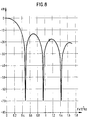
- the Fourier transform S (f) of the impulse response, or frequency response, represented in FIG. 2B is of the sinx / x form already mentioned because this converter 5 has a low-pass filtering function. If the center frequency f 0 is for example 2.25 times the sampling frequency f e , it appears that the attenuation is very important.
- the known solution consists in reducing the width of the impulse to approach the ideal case of the impulse from Dirac.
- the amplitude of the impetus to maintain a constant area which is worth Uref.Te.
- the Fourier transform S (f) of the impulse response, or frequency response, is shown in Figure 3B. We have reduced attenuation but this is still relatively high.
- the object of the present invention is therefore to provide an analog-to-digital converter well suited to processing a signal occupying a frequency band B less than its center frequency f 0 .
- Analog to digital converter receives signal analog input to produce a deviation signal digital. It includes a subtractor to make the difference of the input signal and a reference signal, a conversion chain to produce this deviation signal at from this difference and a feedback loop to produce the reference signal by means of a digital to analog converter which outputs a signal from comparison in response to the deviation signal.
- the input signal being assigned a central frequency
- the feedback loop further includes a displacement to displace the frequency response of the zero frequency digital to analog converter towards the central frequency, this displacement member producing the reference signal from the signal comparison.
- displacement device is a modulator producing the reference signal by modulation of the comparison signal by means of a signal modulating.
- the modulating signal has a spectral component at a modulation frequency equal to the center frequency.
- the signal is the product of the comparison signal and the modulating signal.
- the invention applies naturally when the chain conversion includes a sampler working at a sampling frequency, so the deviation signal keeps a constant value during a period sampling.
- the modulating signal has a spectral component at a frequency of modulation equal to a multiple of half of this sampling frequency.
- the modulating signal has a value positive at the end of each period of samples.
- the conversion chain includes a filter bandpass centered on the center frequency and a quantifier.
- this quantifier is a comparator.
- Sigma-delta converters are generally with two main functions: conversion proper and digital processing including including a filtering and decimation operation.
- the invention relates to the conversion proper, that is to say say the set of organs that get the deviation signal at the output of the quantizer. That is why we will now consider, through an abuse of language, that the analog to digital converter matches these only organs.
- the invention proposes to alleviate the phenomenon mitigation presented above and shown schematically in the figure 2B.
- Provision is made for this to move the main lobe of the frequency response which is the Fourier transform S (f) of the impulse response from the frequency f 0 to the central frequency f 0 by means of a displacement member.
- the sigma-delta converter includes a subtractor 1 which receives an input signal x (t) and a reference signal Ur (t) to tell the difference. It then includes a bandpass filter 2 which receives the output signal from the subtractor 1 to produce a filtered signal, a sampler 3 which receives this filtered signal and produces samples, and a quantifier 4 which delivers a signal numerical deviation y (t) from these samples.
- the quantifier 4 produces a signal on two levels, i.e. it reduced to a comparator.
- the assembly constituted by the filter 2, the sampler 3 and the quantifier 4 provide a function well known to those skilled in the art and we will agree to name it conversion chain.
- the sigma-delta converter also includes a feedback loop. This loop has a digital to analog converter 5 which produces a signal comparison Uc (t) from the deviation signal y (t).
- the feedback loop includes the displacement device which produces the signal reference Ur (t) from the comparison signal Uc (t).
- a low-pass filter can be provided 6 at the output of the digital analog converter 5.
- the function of this filter will be explained later.
- this movement member is a modulator (7) which produces the reference signal Ur (t) by modulating the comparison signal Uc (t) filtered or unfiltered by means of a modulating signal md (t).
- the modulation operation is a multiplication so the reference signal Ur (t) is the product of the comparison signal Uc (t) and the modulating signal md (t).
- the purpose of this modulation is to modify the response frequency of digital to analog converter 5.
- the modulating signal md (t) can be sinusoidal, at which the low-pass filter 6 is of more limited interest. However, it may be more convenient to choose a signal square, to facilitate the realization of modulator 7, by example.
- This modulating signal md (t) is therefore chosen so that it has a spectral component at the modulation frequency f m close to the central frequency f 0 .
- these two frequencies should be equal, but it may be more convenient to adopt different values if only for technological reasons.
- the phase of md (t) is important for the stability of the sigma-delta converter. However, the ambiguity of the phase for cases m> 0 is simple to raise, as has been approached by J.H. DRESSLER in the work already cited.
- the modulating signal m 1 (t) In the first form of the modulating signal m 1 (t), there appears a positive feedback at the end of the sampling period, that is to say between 3T / 2 and Te in the present case. This phenomenon can cause the sigma-delta converter to oscillate.
- An advantageous solution consists in choosing the second form m 2 (t) of the modulating signal to avoid any risk of instability.
- the modulating signal must always have a positive value at the end of a sampling period, that is to say during a possible change in value of the comparison signal Uc (t).
- the coefficient ⁇ and the gain a 0 are determined in order to optimize the noise rejection, while guaranteeing the stability of the sigma-delta converter.
- the entire digital converter analog 5 and the modulator has impulse response h (t).
- H ( ⁇ ), H 0 ( ⁇ ), H 1 ( ⁇ ), H 2 ( ⁇ ) represent the Fourier transforms of the respective functions h (t), h 0 (t), h 1 (t), h 2 (t).
- the module of H ( ⁇ ) is represented in figure 7.
- the converter transfer function module digital analog 5 is shown in figure 8.
- the converter of the invention thus produces an attenuation 6dB instead of approximately 20 dB in the absence of a modulator.
Abstract
Description
La présente invention concerne un convertisseur analogique numérique à boucle de contre-réaction modulée.The present invention relates to a converter analog digital with modulated feedback loop.
Le domaine de l'invention est celui de la conversion d'un signal d'entrée analogique en un signal de sortie numérique dans le cas plus précis où ce signal de sortie doit présenter une haute résolution ou bien lorsque le signal d'entrée présente une grande dynamique.The field of the invention is that of conversion from an analog input signal to an output signal digital in the more precise case where this output signal must have a high resolution or when the input signal has great dynamics.
Dans ce domaine particulier, figurent notamment les systèmes de radiocommunications où le signal d'entrée d'un récepteur peut varier dans une large mesure, de l'ordre de 100 dB ou même plus.In this particular area, notably include radiocommunication systems where the input signal from a receiver can vary widely, on the order of 100 dB or even more.
Il est ainsi connu d'utiliser pour la conversion d'un signal d'entrée en bande de base un convertisseur de type sigma-delta. Ses principaux avantages sont les suivants :
- il a une faible sensibilité aux imperfections des composants,
- il peut être aisément intégré dans un circuit,
- il a une consommation plus faible que ces homologues (convertisseurs flashs) à performances égales,
- il présente une bonne linéarité pour des résolutions importantes.
- it has a low sensitivity to component imperfections,
- it can be easily integrated into a circuit,
- it has a lower consumption than these counterparts (flash converters) with equal performance,
- it presents a good linearity for important resolutions.
Le convertisseur sigma-delta est fréquemment pourvu d'une fonction de filtrage passe-bas. Ainsi, pour un signal d'entrée occupant une largeur de bande B autour d'une fréquence centrale f0, il faut que le filtre passe-bas ait une fréquence de coupure au moins égale à f0 + B/2. On sait que lorsque l'on augmente la fréquence de coupure, on augmente le coût du composant en conséquence. De plus, pour une fréquence d'échantillonnage fe déterminée du convertisseur, si l'on augmente la fréquence de coupure, on dégrade le rapport signal sur bruit.The sigma-delta converter is often provided with a low-pass filtering function. Thus, for an input signal occupying a bandwidth B around a central frequency f 0 , the low-pass filter must have a cut-off frequency at least equal to f 0 + B / 2. We know that when we increase the cutoff frequency, we increase the cost of the component accordingly. In addition, for a determined sampling frequency f e of the converter, if the cutoff frequency is increased, the signal to noise ratio is degraded.
Afin d'améliorer cette situation, on a prévu de remplacer la fonction de filtrage passe-bas par une fonction de filtrage passe-bande. Cette solution est notamment exposée dans l'ouvrage de J.H. DRESSLER : "Interpolative Bandpass A/D Conversion", Signal Processing, Elsevier Science Publishers B.V., 22, pp. 139-151, 1991.In order to improve this situation, provision has been made replace the low-pass filtering function with a function bandpass filtering. This solution is notably exposed in the work of J.H. DRESSLER: "Interpolative Bandpass A / D Conversion ", Signal Processing, Elsevier Science Publishers B.V., 22, pp. 139-151, 1991.
On choisit en général d'adopter comme fréquence centrale du filtre passe-bande la fréquence centrale f0 de la largeur de bande du signal d'entrée. Il se produit alors une atténuation en sinx/x par rapport au convertisseur sigma-delta pourvu d'un filtre passe-bas où x prend la valeur π.f0/fe, ce qui sera explicité par la suite. Il s'ensuit que plus la fréquence centrale f0 du filtre passe-bande est élevée, plus l'atténuation est importante. Naturellement, une augmentation de l'atténuation entraíne une dégradation du rapport signal sur bruit.In general, it is chosen to adopt as the center frequency of the bandpass filter the center frequency f 0 of the bandwidth of the input signal. There is then an attenuation in sinx / x relative to the sigma-delta converter provided with a low-pass filter where x takes the value π.f 0 / f e , which will be explained later. It follows that the higher the center frequency f 0 of the bandpass filter, the greater the attenuation. Naturally, an increase in attenuation leads to a degradation of the signal to noise ratio.
Il existe une solution pour limiter ce phénomène, mais pour l'exposer, il convient auparavant de décrire brièvement le fonctionnement du convertisseur sigma-delta en référence à la figure 1. Celui-ci comprend un soustracteur 1 qui reçoit un signal d'entrée x(t) et un signal de référence Ur(t) pour en faire la différence. Il comprend ensuite un filtre 2 qui reçoit le signal de sortie du soustracteur 1 pour produire un signal filtré, un échantillonneur 3 qui reçoit ce signal filtré et produit des échantillons, et un quantificateur 4 qui délivre un signal d'écart numérique y(t) à partir de ces échantillons. Le convertisseur comprend également une boucle de contre-réaction. Cette boucle comporte un convertisseur numérique analogique 5 qui produit le signal de référence Ur(t) à partir du signal d'écart y(t). Par ailleurs, on admet ici, à titre d'exemple, que le quantificateur 4 produit un signal sur deux niveaux, c'est-à-dire qu'il se réduit à un comparateur.There is a solution to limit this phenomenon, but to expose it, it is first necessary to briefly describe the operation of the sigma-delta converter in reference in Figure 1. This includes a subtractor 1 which receives an input signal x (t) and a reference signal Ur (t) to tell the difference. It then includes a filter 2 which receives the output signal from subtractor 1 to produce a filtered signal, a sampler 3 which receives this filtered signal and produces samples, and a quantizer 4 which outputs a digital deviation signal y (t) from these samples. The converter includes also a feedback loop. This loop includes a digital to analog converter 5 which produces the reference signal Ur (t) from the deviation signal y (t). Furthermore, it is admitted here, by way of example, that the quantizer 4 produces a signal on two levels, i.e. that it is reduced to a comparator.
Le phénomène d'atténuation évoqué ci-dessus est particulièrement marqué lorsque la fréquence d'échantillonnage fe est inférieure à la fréquence centrale f0. En effet, le signal de référence Ur(t) d'amplitude maximale Uref est susceptible de changer de valeur au même rythme que le signal d'écart y(t), c'est-à-dire à chaque période d'échantillonnage Te où Te vaut évidemment l'inverse de la fréquence d'échantillonage fe. Une impulsion en sortie du convertisseur numérique analogique 5 présente ainsi une amplitude Uref pendant une durée Te, comme représenté à la figure 2A. La transformée de Fourier S(f) de la réponse impulsionnelle, ou réponse fréquentielle, représentée dans la figure 2B est de la forme sinx/x déjà évoquée du fait que ce convertisseur 5 a une fonction de filtrage passe-bas. Si la fréquence centrale f0 vaut par exemple 2,25 fois la fréquence d'échantillonnage fe, il apparaít que l'atténuation est très importante.The attenuation phenomenon mentioned above is particularly marked when the sampling frequency f e is less than the central frequency f 0 . Indeed, the reference signal Ur (t) of maximum amplitude Uref is capable of changing value at the same rate as the difference signal y (t), that is to say at each sampling period Te where Te is obviously the inverse of the sampling frequency f e . A pulse at the output of the digital analog converter 5 thus has an amplitude Uref for a duration Te, as shown in FIG. 2A. The Fourier transform S (f) of the impulse response, or frequency response, represented in FIG. 2B is of the sinx / x form already mentioned because this converter 5 has a low-pass filtering function. If the center frequency f 0 is for example 2.25 times the sampling frequency f e , it appears that the attenuation is very important.
La solution connue consiste à réduire la largeur de l'impulsion pour se rapprocher du cas idéal de l'impulsion de Dirac. Cependant, il faut augmenter l'amplitude de l'impulsion pour conserver une aire constante qui vaut Uref.Te. A titre d'exemple, on peut diviser la durée de l'impulsion par 4 et multiplier son amplitude par 4, comme représenté dans la figure 3A. La transformée de Fourier S(f) de la réponse impulsionnelle, ou réponse fréquentielle, est représentée dans la figure 3B. On a bien réduit l'atténuation mais celle-ci est encore relativement élevée.The known solution consists in reducing the width of the impulse to approach the ideal case of the impulse from Dirac. However, the amplitude of the impetus to maintain a constant area which is worth Uref.Te. As an example, we can divide the duration of the pulse by 4 and multiply its amplitude by 4, as shown in Figure 3A. The Fourier transform S (f) of the impulse response, or frequency response, is shown in Figure 3B. We have reduced attenuation but this is still relatively high.
De plus, le fait d'augmenter l'amplitude du signal de référence n'est pas souhaitable pour deux raisons au moins. La première est qu'il faut disposer d'une alimentation d'énergie permettant de le faire. Ce n'est pas toujours le cas, surtout si l'accroissement d'amplitude souhaité est important. La seconde raison est liée au temps de montée tant du convertisseur numérique analogique 5 que de l'étage d'entrée correspondant du soustracteur 1. Si le signal de référence Ur(t) devrait en théorie présenter une pente d(Ur)/dt infinie, ce n'est pas le cas dans la pratique où cette pente a une valeur fixée k. Ainsi, le retard entre un changement de valeur du signal d'écart y(t) et la prise en compte globale de ce changement dans le signal de sortie du soustracteur sera d'autant plus important que l'amplitude du signal de référence est élevée. Il peut même arriver que l'impulsion théorique souhaitée ait un rapport amplitude sur durée qui soit supérieur à cette valeur k, si bien que l'impulsion réelle n'atteindra jamais l'amplitude souhaitée. Il va sans dire que les performances du convertisseur sigma-delta s'en trouvent sérieusement dégradées.In addition, increasing the amplitude of the signal reference is not desirable for at least two reasons. The first is that you have to have a power supply of energy to do it. It is not always the case, especially if the desired amplitude increase is important. The second reason is related to the rise time both of the digital analog converter 5 and of the stage corresponding input of subtractor 1. If the signal reference Ur (t) should theoretically have a slope d (Ur) / dt infinite, this is not the case in practice where this slope has a fixed value k. So the delay between a change in value of the deviation signal y (t) and taking overall account of this change in the output signal of the subtractor will be all the more important as the amplitude of the reference signal is high. It may even happen that the desired theoretical pulse has an amplitude ratio on duration which is greater than this value k, so that the actual impulse will never reach the desired amplitude. It goes without saying that the performance of the sigma-delta converter are seriously degraded.
Il apparaít donc que la solution qui consiste à modifier la forme de l'impulsion n'apporte pas de réponse définitive au problème posé.It therefore appears that the solution which consists in changing the shape of the pulse does not provide an answer definitive to the problem posed.
La présente invention a ainsi pour but un convertisseur analogique numérique bien adapté au traitement d'un signal occupant une bande de fréquences B inférieure à sa fréquence centrale f0.The object of the present invention is therefore to provide an analog-to-digital converter well suited to processing a signal occupying a frequency band B less than its center frequency f 0 .
Le convertisseur analogique numérique reçoit un signal d'entrée analogique pour produire un signal d'écart numérique. Il comprend un soustracteur pour faire la différence du signal d'entrée et d'un signal de référence, une chaíne de conversion pour produire ce signal d'écart à partir de cette différence et une boucle de contre-réaction pour produire le signal de référence au moyen d'un convertisseur numérique analogique qui délivre un signal de comparaison en réponse au signal d'écart. Selon l'invention, le signal d'entrée étant affecté d'une fréquence centrale, la boucle de contre-réaction comprend de plus un organe de déplacement pour déplacer la réponse fréquentielle du convertisseur numérique analogique de la fréquence nulle vers la fréquence centrale, cet organe de déplacement produisant le signal de référence à partir du signal de comparaison.Analog to digital converter receives signal analog input to produce a deviation signal digital. It includes a subtractor to make the difference of the input signal and a reference signal, a conversion chain to produce this deviation signal at from this difference and a feedback loop to produce the reference signal by means of a digital to analog converter which outputs a signal from comparison in response to the deviation signal. According to the invention, the input signal being assigned a central frequency, the feedback loop further includes a displacement to displace the frequency response of the zero frequency digital to analog converter towards the central frequency, this displacement member producing the reference signal from the signal comparison.
Dans un mode de réalisation avantageux du convertisseur analogique numérique, l'organe de déplacement est un modulateur produisant le signal de référence par modulation du signal de comparaison au moyen d'un signal modulant.In an advantageous embodiment of the analog-to-digital converter, displacement device is a modulator producing the reference signal by modulation of the comparison signal by means of a signal modulating.
On obtient ainsi un moyen commode de parvenir au résultat souhaité, à savoir une diminution de l'atténuation et, par conséquent, une amélioration des performances du convertisseur analogique numérique.This provides a convenient way to reach the desired result, i.e. reduced attenuation and therefore an improvement in the performance of the analog to digital converter.
Selon une première option, on peut prévoir que le signal modulant présente une composante spectrale à une fréquence de modulation égale à la fréquence centrale.According to a first option, it can be foreseen that the modulating signal has a spectral component at a modulation frequency equal to the center frequency.
Par ailleurs, suivant une solution simple, le signal de référence est le produit du signal de comparaison et du signal modulant.Furthermore, according to a simple solution, the signal is the product of the comparison signal and the modulating signal.
L'invention s'applique naturellement lorsque la chaíne de conversion comprend un échantillonneur travaillant à une fréquence d'échantillonnage, de sorte que le signal d'écart garde une valeur constante durant une période d'échantillonnage.The invention applies naturally when the chain conversion includes a sampler working at a sampling frequency, so the deviation signal keeps a constant value during a period sampling.
Ainsi, selon une seconde option, le signal modulant présente une composante spectrale à une fréquence de modulation égale à un multiple de la moitié de cette fréquence d'échantillonnage.Thus, according to a second option, the modulating signal has a spectral component at a frequency of modulation equal to a multiple of half of this sampling frequency.
On prévoit de plus que le signal modulant a une valeur positive à la fin de chacune des périodes d'échantillonnages.It is further expected that the modulating signal has a value positive at the end of each period of samples.
En outre, la chaíne de conversion comprend un filtre passe-bande centré sur la fréquence centrale et un quantificateur.In addition, the conversion chain includes a filter bandpass centered on the center frequency and a quantifier.
Avantageusement, ce quantificateur est un comparateur.Advantageously, this quantifier is a comparator.
En tout état de cause, on peut ajouter un filtre passe-bas entre le convertisseur numérique analogique et l'organe de déplacement.In any event, we can add a filter low pass between digital to analog converter and the displacement member.
L'invention apparaítra maintenant de manière plus précise dans le cadre de la description qui suit en référence aux figures annexées qui représentent :
- la figure 1, un convertisseur analogique numérique de l'état de l'art,
- les figures 2A et 2B, respectivement une impulsion calibrée et la transformée de Fourier de la réponse impulsionnelle d'un élément de ce convertisseur selon un premier mode de réalisation connu,
- les figures 3A et 3B, respectivement une impulsion calibrée et la transformée de Fourier de la réponse impulsionnelle d'un élément de ce convertisseur selon un second mode de réalisation connu,
- la figure 4, un exemple d'un convertisseur analogique numérique selon l'invention,
- la figure 5, la forme du signal de comparaison et du signal modulant mis en oeuvre dans ce convertisseur,
- la figure 6, un schéma de la réponse impulsionnelle de la boucle de contre-réaction de ce convertisseur,
- la figure 7, un diagramme du module de la fonction de transfert de cette boucle,
- la figure 8, un diagramme du module de la fonction de transfert d'un élément de cette boucle.
- FIG. 1, a state-of-the-art analog-to-digital converter,
- FIGS. 2A and 2B, respectively a calibrated pulse and the Fourier transform of the impulse response of an element of this converter according to a first known embodiment,
- FIGS. 3A and 3B, respectively a calibrated pulse and the Fourier transform of the impulse response of an element of this converter according to a second known embodiment,
- FIG. 4, an example of an analog to digital converter according to the invention,
- FIG. 5, the form of the comparison signal and the modulating signal used in this converter,
- FIG. 6, a diagram of the impulse response of the feedback loop of this converter,
- FIG. 7, a diagram of the module of the transfer function of this loop,
- FIG. 8, a diagram of the module of the transfer function of an element of this loop.
Les éléments présents dans différentes figures seront affectés d'une seule référence.The elements present in different figures will assigned a single reference.
Les convertisseurs sigma-delta sont généralement pourvus de deux fonctions principales : la conversion proprement dite et un traitement numérique comprenant notamment une opération de filtrage et de décimation. L'invention concerne la conversion proprement dite, c'est-à dire l'ensemble des organes qui permettent d'obtenir le signal d'écart à la sortie du quantificateur. C'est pourquoi on considèrera dorénavant, par un abus de langage, que le convertisseur analogique numérique correspond à ces seuls organes.Sigma-delta converters are generally with two main functions: conversion proper and digital processing including including a filtering and decimation operation. The invention relates to the conversion proper, that is to say say the set of organs that get the deviation signal at the output of the quantizer. That is why we will now consider, through an abuse of language, that the analog to digital converter matches these only organs.
L'invention se propose de pallier au phénomène d'atténuation présenté plus haut et schématisé sur la figure 2B.The invention proposes to alleviate the phenomenon mitigation presented above and shown schematically in the figure 2B.
On prévoit pour ce faire de déplacer le lobe principal de la réponse fréquentielle qui est la transformée de Fourier S(f) de la réponse impulsionnelle de la fréquence f = 0 vers la fréquence centrale f0 au moyen d'un organe de déplacement.Provision is made for this to move the main lobe of the frequency response which is the Fourier transform S (f) of the impulse response from the frequency f = 0 to the central frequency f 0 by means of a displacement member.
De manière connue, en référence à la figure 4, le convertisseur sigma-delta comprend un soustracteur 1 qui reçoit un signal d'entrée x(t) et un signal de référence Ur(t) pour en faire la différence. Il comprend ensuite un filtre passe-bande 2 qui reçoit le signal de sortie du soustracteur 1 pour produire un signal filtré, un échantillonneur 3 qui reçoit ce signal filtré et produit des échantillons, et un quantificateur 4 qui délivre un signal d'écart numérique y(t) à partir de ces échantillons. On admet ici, à titre d'exemple, que le quantificateur 4 produit un signal sur deux niveaux, c'est-à-dire qu'il se réduit à un comparateur. L'ensemble constitué par le filtre 2, l'échantillonneur 3 et le quantificateur 4 assure une fonction bien connue de l'homme du métier et l'on conviendra de le nommer chaine de conversion.In known manner, with reference to FIG. 4, the sigma-delta converter includes a subtractor 1 which receives an input signal x (t) and a reference signal Ur (t) to tell the difference. It then includes a bandpass filter 2 which receives the output signal from the subtractor 1 to produce a filtered signal, a sampler 3 which receives this filtered signal and produces samples, and a quantifier 4 which delivers a signal numerical deviation y (t) from these samples. We here admits, by way of example, that the quantifier 4 produces a signal on two levels, i.e. it reduced to a comparator. The assembly constituted by the filter 2, the sampler 3 and the quantifier 4 provide a function well known to those skilled in the art and we will agree to name it conversion chain.
Le convertisseur sigma-delta comprend également une boucle de contre-réaction. Cette boucle comporte un convertisseur numérique analogique 5 qui produit un signal de comparaison Uc(t) à partir du signal d'écart y(t).The sigma-delta converter also includes a feedback loop. This loop has a digital to analog converter 5 which produces a signal comparison Uc (t) from the deviation signal y (t).
Selon l'invention, la boucle de contre-réaction comprend l'organe de déplacement qui produit le signal de référence Ur(t) à partir du signal de comparaison Uc(t).According to the invention, the feedback loop includes the displacement device which produces the signal reference Ur (t) from the comparison signal Uc (t).
A titre optionnel, on peut prévoir un filtre passe-bas 6 à la sortie du convertisseur numérique analogique 5. La fonction de ce filtre sera explicitée par la suite.Optionally, a low-pass filter can be provided 6 at the output of the digital analog converter 5. The function of this filter will be explained later.
On va maintenant décrire un exemple de réalisation de cet organe de déplacement : il s'agit dun modulateur (7) qui produit le signal de référence Ur(t) par modulation du signal de comparaison Uc(t) filtré ou non filtré au moyen d'un signal modulant md(t).We will now describe an embodiment of this movement member: it is a modulator (7) which produces the reference signal Ur (t) by modulating the comparison signal Uc (t) filtered or unfiltered by means of a modulating signal md (t).
Dans l'exemple adopté ici, l'opération de modulation est une multiplication de sorte que le signal de référence Ur(t) vaut le produit du signal de comparaison Uc(t) et du signal modulant md(t).In the example adopted here, the modulation operation is a multiplication so the reference signal Ur (t) is the product of the comparison signal Uc (t) and the modulating signal md (t).
Cette modulation a pour objet de modifier la réponse fréquentielle du convertisseur numérique analogique 5.The purpose of this modulation is to modify the response frequency of digital to analog converter 5.
Le signal modulant md(t) peut être sinusoïdal, auquel cas le filtre passe-bas 6 présente un intérêt plus limité. Cependant, il peut être plus commode de choisir un signal carré, afin de faciliter la réalisation du modulateur 7, par exemple.The modulating signal md (t) can be sinusoidal, at which the low-pass filter 6 is of more limited interest. However, it may be more convenient to choose a signal square, to facilitate the realization of modulator 7, by example.
Dans ce dernier cas, le modulateur 7 va déplacer vers la fréquence du signal modulant md(t) qu'on nomme fréquence de modulation fm :
- le lobe principal de S(f) suite à l'effet de la composante fondamentale du signal modulant,
- des lobes secondaires suite au produit des harmoniques de ce signal modulant et des lobes secondaires de S(f).
- the main lobe of S (f) following the effect of the fundamental component of the modulating signal,
- secondary lobes following the product of the harmonics of this modulating signal and secondary lobes of S (f).
Ces lobes secondaires peuvent être considérés comme un bruit. C'est ici que le filtre passe-bas 6 prend tout son intérêt, pour éliminer ce bruit indésirable.These side lobes can be considered a noise. This is where the low pass filter 6 takes its full effect interest, to eliminate this unwanted noise.
On choisit donc ce signal modulant md(t) pour qu'il ait une composante spectrale à la fréquence de modulation fm proche de la fréquence centrale f0. Dans l'idéal, il conviendrait que ces deux fréquences soient égales, mais il peut être plus commode d'adopter des valeurs différentes ne serait-ce que pour des raisons technologiques.This modulating signal md (t) is therefore chosen so that it has a spectral component at the modulation frequency f m close to the central frequency f 0 . Ideally, these two frequencies should be equal, but it may be more convenient to adopt different values if only for technological reasons.
En effet, compte-tenu du fait qu'il est déjà prévu un
générateur d'horloge pour produire la fréquence
d'échantilonnage fe, une solution avantageuse consiste à
choisir la fréquence de modulation fm comme un multiple de
la moitié de cette fréquence d'échantillonnage :
La phase de md(t) est importante pour la stabilité du convertisseur sigma-delta. Cependant, l'ambiguïté de la phase pour les cas m>0 est simple à lever, comme cela a été abordé par J.H. DRESSLER dans l'ouvrage déjà cité. Le signal md(t) est considéré synchrone de la fréquence d'échantillonnage fe. Deux cas sont à envisager comme indiqué dans la figure 5 où l'on a choisi m = 4 à titre d'exemple.The phase of md (t) is important for the stability of the sigma-delta converter. However, the ambiguity of the phase for cases m> 0 is simple to raise, as has been approached by J.H. DRESSLER in the work already cited. The signal md (t) is considered synchronous with the frequency sampling fe. Two cases are to be considered as indicated in figure 5 where we chose m = 4 as example.
On a représenté le signal de comparaison Uc(t) et deux formes possibles du signal modulant :
- la première m1(t) où ce signal est en phase avec le signal de comparaison,
- la seconde m2(t) où ce signal est en opposition de phase avec le signal de comparaison.
- the first m 1 (t) where this signal is in phase with the comparison signal,
- the second m 2 (t) where this signal is in phase opposition with the comparison signal.
Dans la première forme du signal modulant m1(t), il apparait une contre-réaction positive à la fin de la période d'échantillonnage, c'est-à-dire entre 3T/2 et Te dans le cas présent. Ce phénomène peut provoquer une oscillation du convertisseur sigma-delta. Une solution avantageuse consiste à choisir la seconde forme m2(t) du signal modulant pour éviter tout risque d'instabilité. En fin de compte, le signal modulant doit toujours avoir une valeur positive à la fin d'une période d'échantillonnage, c'est-à-dire lors d'un possible changement de valeur du signal de comparaison Uc(t).In the first form of the modulating signal m 1 (t), there appears a positive feedback at the end of the sampling period, that is to say between 3T / 2 and Te in the present case. This phenomenon can cause the sigma-delta converter to oscillate. An advantageous solution consists in choosing the second form m 2 (t) of the modulating signal to avoid any risk of instability. Ultimately, the modulating signal must always have a positive value at the end of a sampling period, that is to say during a possible change in value of the comparison signal Uc (t).
On rappellera maintenant l'expression connue de la
fonction de transfert G(p) d'un filtre passe-bas d'ordre 2 :

On peut convertir ce filtre passe-bas pour obtenir le
filtre passe-bande 2 du convertisseur sigma-delta par le
biais d'une transformation X(p), par exemple :
L'expression du filtre passe-bande F(p) correspondant
d'ordre 4 devient donc :
Le coefficient α et le gain a0 sont déterminés afin d'optimiser la réjection du bruit, tout en garantissant la stabilité du convertisseur sigma-delta. The coefficient α and the gain a 0 are determined in order to optimize the noise rejection, while guaranteeing the stability of the sigma-delta converter.
Par ailleurs, l'ensemble du convertisseur numérique analogique 5 et du modulateur a pour réponse impulsionnelle h(t).In addition, the entire digital converter analog 5 and the modulator has impulse response h (t).
On adopte les notations suivantes en référence à la figure 6 :
- h0(t) est un signal élémentaire qui correspond à une impulsion de durée T/2 centrée sur l'origine des temps,
- h1(t) est un premier signal de combinaison qui correspond aux impulsions négatives de h(t), et
- h2(t) est un second signal de combinaison qui correspond aux impulsions positives de h(t).
- h 0 (t) is an elementary signal which corresponds to a pulse of duration T / 2 centered on the origin of the times,
- h 1 (t) is a first combination signal which corresponds to the negative pulses of h (t), and
- h 2 (t) is a second combination signal which corresponds to the positive pulses of h (t).
Par convention, H(ω), H0(ω), H1(ω), H2(ω) représentent les transformées de Fourier des fonctions respectives h(t), h0(t), h1(t), h2(t).By convention, H (ω), H 0 (ω), H 1 (ω), H 2 (ω) represent the Fourier transforms of the respective functions h (t), h 0 (t), h 1 (t), h 2 (t).
On peut alors écrire :


On donne l'application numérique suivante en matière
d'exemple :
L'expression du filtre passe-bande F(p) a été déterminée en utilisant la formule (1). Son expression est obtenue en prenant a0 = 1 et α = 0.5.The expression of the bandpass filter F (p) was determined using formula (1). Its expression is obtained by taking a 0 = 1 and α = 0.5.
La fonction de transfert de l'ensemble du
convertisseur numérique analogique 5 et du modulateur 7 a
pour expression, selon la formule (2) :

Le module de H(ω) est représenté dans la figure 7. Le module de la fonction de transfert du convertisseur numérique analogique 5 est représenté dans la figure 8. Le convertisseur de l'invention produit ainsi une atténuation de 6dB au lieu de 20 dB environ en l'absence de modulateur.The module of H (ω) is represented in figure 7. The converter transfer function module digital analog 5 is shown in figure 8. The converter of the invention thus produces an attenuation 6dB instead of approximately 20 dB in the absence of a modulator.
Claims (11)
- Analogue-to-digital converter receiving an analogue input signal (x(t)) to produce a digital error signal (y(t)) comprising a subtractor (1) to calculate the difference between said input signal and a reference signal (Ur(t)), a converter subsystem (2, 3, 4) to produce said error signal from said difference and a feedback loop to produce said reference signal by means of a digital-to-analogue converter (5) which delivers a comparison signal (Uc(t)) in response to said error signal, characterised in that, said input signal (x(t)) being assigned a centre frequency (f0), said feedback loop comprises a displacement unit (7) for displacing the frequency response of said digital-to-analogue converter (5) from the null frequency towards said centre frequency (f0), said displacement unit producing said reference signal (Ur(t)) from said comparison signal (Uc(t)).
- Analogue-to-digital converter according to claim 1 characterised in that said displacement unit is a modulator (7) producing said reference signal (Ur(t)) by modulating said comparison signal (Uc(t)) by means of a modulating signal (md(t)).
- Analogue-to-digital converter according to claim 2 characterised in that said modulating signal (md(t)) has a spectral component at a modulation frequency (fm) equal to said centre frequency (f0).
- Analogue-to-digital converter according to claim 2 characterised in that said reference signal (Ur(t)) is the product of said comparison signal (Uc(t)) and said modulating signal (md(t)).
- Analogue-to-digital converter according to claim 4 characterised in that said converter subsystem comprises a sampler (3) operating at a sampling frequency (fe) whereby said error signal (y(t)) retains a constant value during a sampling period (Te).
- Analogue-to-digital converter according to claim 5 characterised in that said modulating signal (md(t)) has a spectral component at a modulation frequency (fm) equal to a multiple of half said sampling frequency (fe).
- Analogue-to-digital converter according to claim 5 characterised in that said modulating signal (md(t)) has a positive value at the end of each sampling period.
- Analogue-to-digital converter according to claim 5 characterised in that said converter subsystem comprises a bandpass filter (2) centred on said centre frequency (f0).
- Analogue-to-digital converter according to claim 5 characterised in that said converter subsystem comprises a quantizer (4).
- Analogue-to-digital converter according to claim 9 characterised in that said quantizer (4) is a comparator.
- Analogue-to-digital converter according to any one of the preceding claims characterised in that it comprises a lowpass filter (6) between said digital-to-analogue converter (5) and said displacement unit (7).
Applications Claiming Priority (2)
| Application Number | Priority Date | Filing Date | Title |
|---|---|---|---|
| FR9308625A FR2707815B1 (en) | 1993-07-13 | 1993-07-13 | Analog to digital converter with modulated feedback loop. |
| FR9308625 | 1993-07-13 |
Publications (2)
| Publication Number | Publication Date |
|---|---|
| EP0635946A1 EP0635946A1 (en) | 1995-01-25 |
| EP0635946B1 true EP0635946B1 (en) | 1998-09-30 |
Family
ID=9449225
Family Applications (1)
| Application Number | Title | Priority Date | Filing Date |
|---|---|---|---|
| EP94401587A Expired - Lifetime EP0635946B1 (en) | 1993-07-13 | 1994-07-08 | Analog to digital converter with modulated feedback |
Country Status (8)
| Country | Link |
|---|---|
| US (1) | US5565868A (en) |
| EP (1) | EP0635946B1 (en) |
| JP (1) | JP3212222B2 (en) |
| AT (1) | ATE171828T1 (en) |
| DE (1) | DE69413617T2 (en) |
| ES (1) | ES2124860T3 (en) |
| FI (1) | FI943289A (en) |
| FR (1) | FR2707815B1 (en) |
Families Citing this family (11)
| Publication number | Priority date | Publication date | Assignee | Title |
|---|---|---|---|---|
| JP3310114B2 (en) * | 1994-09-14 | 2002-07-29 | 株式会社東芝 | A / D converter having frequency conversion function and wireless device using the same |
| US7218448B1 (en) * | 1997-03-17 | 2007-05-15 | The Regents Of The University Of Colorado | Extended depth of field optical systems |
| DE19701844A1 (en) * | 1997-01-21 | 1998-07-23 | Motorola Inc | Interference signal suppression filter |
| US6121910A (en) * | 1998-07-17 | 2000-09-19 | The Trustees Of Columbia University In The City Of New York | Frequency translating sigma-delta modulator |
| JP3504158B2 (en) | 1998-09-29 | 2004-03-08 | 株式会社東芝 | A / D converter having frequency conversion function and wireless device using the same |
| US7072412B1 (en) | 1999-11-09 | 2006-07-04 | Maurice Bellanger | Multicarrier digital transmission system using an OQAM transmultiplexer |
| CN1513226A (en) * | 2001-05-01 | 2004-07-14 | ��������ͨ�Ź�ҵ��˾ | Frequency switching under sampling |
| US6611222B1 (en) | 2002-06-03 | 2003-08-26 | Charles Douglas Murphy | Low-complexity high-speed analog-to-digital converters |
| DE102006023697B4 (en) * | 2006-05-19 | 2008-02-07 | Infineon Technologies Ag | Method of decoding, decoder, encoder-decoder system and converter |
| EP3386394A1 (en) | 2015-12-10 | 2018-10-17 | Koninklijke Philips N.V. | An ultrasound imaging system probe and system, and an imaging method |
| US11894864B2 (en) * | 2022-03-23 | 2024-02-06 | Silicon Laboratories Inc. | Analog-to-digital converter having punctured quantizer |
Family Cites Families (6)
| Publication number | Priority date | Publication date | Assignee | Title |
|---|---|---|---|---|
| DE2849001C2 (en) * | 1978-11-11 | 1982-10-07 | TE KA DE Felten & Guilleaume Fernmeldeanlagen GmbH, 8500 Nürnberg | Network for adaptive delta modulation |
| US5039909A (en) * | 1989-04-24 | 1991-08-13 | U.S. Philips Corporation | Electric lamp and holder for such a lamp |
| EP0399738A3 (en) * | 1989-05-26 | 1991-05-08 | Gec-Marconi Limited | Analogue to digital converter |
| JP3048263B2 (en) * | 1991-09-02 | 2000-06-05 | 株式会社日立製作所 | Analog / digital converter |
| US5351048A (en) * | 1992-04-09 | 1994-09-27 | Yoshio Yamasaki | One bit high speed signal processing system utilizing controlled spectrum of quantization noise |
| US5257026A (en) * | 1992-04-17 | 1993-10-26 | Crystal Semiconductor, Inc. | Method and apparatus for calibrating a multi-bit delta-sigma modular |
-
1993
- 1993-07-13 FR FR9308625A patent/FR2707815B1/en not_active Expired - Fee Related
-
1994
- 1994-07-08 ES ES94401587T patent/ES2124860T3/en not_active Expired - Lifetime
- 1994-07-08 DE DE69413617T patent/DE69413617T2/en not_active Expired - Fee Related
- 1994-07-08 EP EP94401587A patent/EP0635946B1/en not_active Expired - Lifetime
- 1994-07-08 AT AT94401587T patent/ATE171828T1/en not_active IP Right Cessation
- 1994-07-11 FI FI943289A patent/FI943289A/en unknown
- 1994-07-12 US US08/273,802 patent/US5565868A/en not_active Expired - Fee Related
- 1994-07-13 JP JP16158794A patent/JP3212222B2/en not_active Expired - Fee Related
Also Published As
| Publication number | Publication date |
|---|---|
| ATE171828T1 (en) | 1998-10-15 |
| DE69413617T2 (en) | 1999-03-11 |
| DE69413617D1 (en) | 1998-11-05 |
| JP3212222B2 (en) | 2001-09-25 |
| EP0635946A1 (en) | 1995-01-25 |
| FI943289A0 (en) | 1994-07-11 |
| FI943289A (en) | 1995-01-14 |
| FR2707815A1 (en) | 1995-01-20 |
| FR2707815B1 (en) | 1995-08-25 |
| JPH07170189A (en) | 1995-07-04 |
| US5565868A (en) | 1996-10-15 |
| ES2124860T3 (en) | 1999-02-16 |
Similar Documents
| Publication | Publication Date | Title |
|---|---|---|
| EP1646147B1 (en) | Analog filter for time discrete signals based on passive components | |
| EP0635946B1 (en) | Analog to digital converter with modulated feedback | |
| FR2702902A1 (en) | Digital intermediate frequency receiver and baseband filtering method implemented in this receiver. | |
| EP2360839A1 (en) | Continuous-time analogue-to-digital converter | |
| GB2233518A (en) | Analogue to digital converters | |
| FR2743960A1 (en) | High resolution digital=analog converter for quartz oscillator tuning | |
| EP3053274B1 (en) | Continuous-time quantization device, radio frequency signal receiver comprising such a device and continuous-time quantization method | |
| FR2826207A1 (en) | Passband sigma-delta analog-to-digital converter for a private mobile radio communication system includes multiple adder and resonator system | |
| FR2618960A1 (en) | LINEAR NON-LINEAR ADAPTIVE FREQUENCY FILTER WITH LOW DEPHASING | |
| EP3048730B1 (en) | Frequency synthesis device with feedback loop | |
| EP3276833A1 (en) | Sigma-delta converter with high linearity | |
| EP1514352B1 (en) | Delay-locked loop | |
| EP0246135B1 (en) | Phase frequency detector and its use in a phase-locked loop | |
| FR2805683A1 (en) | METHOD AND DEVICE FOR ANALOGUE / DIGITAL CONVERSION OF A SIGNAL | |
| EP1077530B1 (en) | Method and arrangement for the conversion of an analogue signal into a digital signal with automatic gain control | |
| FR2502872A1 (en) | CARRIER RECOVERY ARRANGEMENT FOR MDP2 OR MDP4 MODULATING SIGNAL | |
| EP2383892B1 (en) | Quantification device, radiofrequency signal receiver including said device and quantification method. | |
| EP1156586B1 (en) | Pipelined analogue-to-digital converter with noise-shaping | |
| EP1014637A1 (en) | Direct conversion receiver for FSK modulated signals | |
| FR2907987A1 (en) | Analog-to-digital converter controlling device for hyperfrequency electronic field, has summing element summing compensation noise to input signal of loop, where noise is equal to signal multiplied by multiplicative noise of converter | |
| FR2999836A1 (en) | Method for conversion of digital signal into analog signal by pulse width modulation, involves generating binary digital by generation of periods, and providing clock signals for specific width of N-bits corresponding to set of clock ticks | |
| WO2002005450A1 (en) | Method for receiving a signal transmitted via a power distribution network and device therefor | |
| FR3091964A1 (en) | Device for generating a modulated signal and associated radiofrequency transmission chain | |
| FR2633127A1 (en) | Method of modulating a single side band signal and modulator by which the method is implemented | |
| FR2484153A1 (en) | SAW recursive filter for mobile telecommunications - has two transducers forming delay line with loop with amplifier and additional transducer connected to filter output |
Legal Events
| Date | Code | Title | Description |
|---|---|---|---|
| PUAI | Public reference made under article 153(3) epc to a published international application that has entered the european phase |
Free format text: ORIGINAL CODE: 0009012 |
|
| AK | Designated contracting states |
Kind code of ref document: A1 Designated state(s): AT BE CH DE DK ES FR GB IT LI NL SE |
|
| 17P | Request for examination filed |
Effective date: 19950616 |
|
| GRAG | Despatch of communication of intention to grant |
Free format text: ORIGINAL CODE: EPIDOS AGRA |
|
| 17Q | First examination report despatched |
Effective date: 19971124 |
|
| GRAG | Despatch of communication of intention to grant |
Free format text: ORIGINAL CODE: EPIDOS AGRA |
|
| GRAH | Despatch of communication of intention to grant a patent |
Free format text: ORIGINAL CODE: EPIDOS IGRA |
|
| GRAH | Despatch of communication of intention to grant a patent |
Free format text: ORIGINAL CODE: EPIDOS IGRA |
|
| GRAA | (expected) grant |
Free format text: ORIGINAL CODE: 0009210 |
|
| RAP1 | Party data changed (applicant data changed or rights of an application transferred) |
Owner name: ALCATEL ALSTHOM COMPAGNIE GENERALE D'ELECTRICITE |
|
| AK | Designated contracting states |
Kind code of ref document: B1 Designated state(s): AT BE CH DE DK ES FR GB IT LI NL SE |
|
| PG25 | Lapsed in a contracting state [announced via postgrant information from national office to epo] |
Ref country code: NL Free format text: LAPSE BECAUSE OF FAILURE TO SUBMIT A TRANSLATION OF THE DESCRIPTION OR TO PAY THE FEE WITHIN THE PRESCRIBED TIME-LIMIT Effective date: 19980930 Ref country code: AT Free format text: LAPSE BECAUSE OF FAILURE TO SUBMIT A TRANSLATION OF THE DESCRIPTION OR TO PAY THE FEE WITHIN THE PRESCRIBED TIME-LIMIT Effective date: 19980930 |
|
| REF | Corresponds to: |
Ref document number: 171828 Country of ref document: AT Date of ref document: 19981015 Kind code of ref document: T |
|
| REG | Reference to a national code |
Ref country code: CH Ref legal event code: EP |
|
| GBT | Gb: translation of ep patent filed (gb section 77(6)(a)/1977) |
Effective date: 19981009 |
|
| REF | Corresponds to: |
Ref document number: 69413617 Country of ref document: DE Date of ref document: 19981105 |
|
| PG25 | Lapsed in a contracting state [announced via postgrant information from national office to epo] |
Ref country code: DK Free format text: LAPSE BECAUSE OF FAILURE TO SUBMIT A TRANSLATION OF THE DESCRIPTION OR TO PAY THE FEE WITHIN THE PRESCRIBED TIME-LIMIT Effective date: 19981231 |
|
| REG | Reference to a national code |
Ref country code: ES Ref legal event code: FG2A Ref document number: 2124860 Country of ref document: ES Kind code of ref document: T3 |
|
| RAP4 | Party data changed (patent owner data changed or rights of a patent transferred) |
Owner name: ALCATEL |
|
| NLV1 | Nl: lapsed or annulled due to failure to fulfill the requirements of art. 29p and 29m of the patents act | ||
| RAP4 | Party data changed (patent owner data changed or rights of a patent transferred) |
Owner name: ALCATEL |
|
| PG25 | Lapsed in a contracting state [announced via postgrant information from national office to epo] |
Ref country code: LI Free format text: LAPSE BECAUSE OF NON-PAYMENT OF DUE FEES Effective date: 19990731 Ref country code: CH Free format text: LAPSE BECAUSE OF NON-PAYMENT OF DUE FEES Effective date: 19990731 Ref country code: BE Free format text: LAPSE BECAUSE OF NON-PAYMENT OF DUE FEES Effective date: 19990731 |
|
| PLBE | No opposition filed within time limit |
Free format text: ORIGINAL CODE: 0009261 |
|
| STAA | Information on the status of an ep patent application or granted ep patent |
Free format text: STATUS: NO OPPOSITION FILED WITHIN TIME LIMIT |
|
| 26N | No opposition filed | ||
| REG | Reference to a national code |
Ref country code: FR Ref legal event code: CD |
|
| BERE | Be: lapsed |
Owner name: ALCATEL ALSTHOM CIE GENERALE D'ELECTRICITE Effective date: 19990731 |
|
| REG | Reference to a national code |
Ref country code: CH Ref legal event code: PL |
|
| PGFP | Annual fee paid to national office [announced via postgrant information from national office to epo] |
Ref country code: SE Payment date: 20010702 Year of fee payment: 8 |
|
| REG | Reference to a national code |
Ref country code: GB Ref legal event code: IF02 |
|
| PG25 | Lapsed in a contracting state [announced via postgrant information from national office to epo] |
Ref country code: SE Free format text: LAPSE BECAUSE OF NON-PAYMENT OF DUE FEES Effective date: 20020709 |
|
| EUG | Se: european patent has lapsed | ||
| PGFP | Annual fee paid to national office [announced via postgrant information from national office to epo] |
Ref country code: ES Payment date: 20030717 Year of fee payment: 10 |
|
| PGFP | Annual fee paid to national office [announced via postgrant information from national office to epo] |
Ref country code: GB Payment date: 20040618 Year of fee payment: 11 |
|
| PGFP | Annual fee paid to national office [announced via postgrant information from national office to epo] |
Ref country code: FR Payment date: 20040623 Year of fee payment: 11 |
|
| PG25 | Lapsed in a contracting state [announced via postgrant information from national office to epo] |
Ref country code: ES Free format text: LAPSE BECAUSE OF NON-PAYMENT OF DUE FEES Effective date: 20040709 |
|
| PGFP | Annual fee paid to national office [announced via postgrant information from national office to epo] |
Ref country code: DE Payment date: 20040715 Year of fee payment: 11 |
|
| PG25 | Lapsed in a contracting state [announced via postgrant information from national office to epo] |
Ref country code: IT Free format text: LAPSE BECAUSE OF NON-PAYMENT OF DUE FEES Effective date: 20050708 Ref country code: GB Free format text: LAPSE BECAUSE OF NON-PAYMENT OF DUE FEES Effective date: 20050708 |
|
| REG | Reference to a national code |
Ref country code: ES Ref legal event code: FD2A Effective date: 20040709 |
|
| PG25 | Lapsed in a contracting state [announced via postgrant information from national office to epo] |
Ref country code: DE Free format text: LAPSE BECAUSE OF NON-PAYMENT OF DUE FEES Effective date: 20060201 |
|
| GBPC | Gb: european patent ceased through non-payment of renewal fee |
Effective date: 20050708 |
|
| PG25 | Lapsed in a contracting state [announced via postgrant information from national office to epo] |
Ref country code: FR Free format text: LAPSE BECAUSE OF NON-PAYMENT OF DUE FEES Effective date: 20060331 |
|
| REG | Reference to a national code |
Ref country code: FR Ref legal event code: ST Effective date: 20060331 |