EP0635741A2 - Optoelektronische Überbrückung und Verfahren zu ihrer Herstellung - Google Patents
Optoelektronische Überbrückung und Verfahren zu ihrer Herstellung Download PDFInfo
- Publication number
- EP0635741A2 EP0635741A2 EP94109901A EP94109901A EP0635741A2 EP 0635741 A2 EP0635741 A2 EP 0635741A2 EP 94109901 A EP94109901 A EP 94109901A EP 94109901 A EP94109901 A EP 94109901A EP 0635741 A2 EP0635741 A2 EP 0635741A2
- Authority
- EP
- European Patent Office
- Prior art keywords
- photonic device
- optical
- optoelectronic interface
- interconnect substrate
- working portion
- Prior art date
- Legal status (The legal status is an assumption and is not a legal conclusion. Google has not performed a legal analysis and makes no representation as to the accuracy of the status listed.)
- Granted
Links
- 230000005693 optoelectronics Effects 0.000 title claims description 38
- 238000004519 manufacturing process Methods 0.000 title description 15
- 230000003287 optical effect Effects 0.000 claims abstract description 66
- 239000013307 optical fiber Substances 0.000 claims abstract description 34
- 239000000758 substrate Substances 0.000 claims abstract description 18
- 238000005253 cladding Methods 0.000 claims description 5
- 238000000034 method Methods 0.000 description 14
- 230000008878 coupling Effects 0.000 description 9
- 238000010168 coupling process Methods 0.000 description 9
- 238000005859 coupling reaction Methods 0.000 description 9
- 238000000465 moulding Methods 0.000 description 4
- 239000000463 material Substances 0.000 description 3
- 230000008569 process Effects 0.000 description 3
- 239000004593 Epoxy Substances 0.000 description 2
- 230000008901 benefit Effects 0.000 description 2
- PCHJSUWPFVWCPO-UHFFFAOYSA-N gold Chemical compound [Au] PCHJSUWPFVWCPO-UHFFFAOYSA-N 0.000 description 2
- 239000010931 gold Substances 0.000 description 2
- 229910052737 gold Inorganic materials 0.000 description 2
- 238000003491 array Methods 0.000 description 1
- 230000005540 biological transmission Effects 0.000 description 1
- 239000003990 capacitor Substances 0.000 description 1
- 239000000919 ceramic Substances 0.000 description 1
- 125000003700 epoxy group Chemical group 0.000 description 1
- 239000000835 fiber Substances 0.000 description 1
- 238000010348 incorporation Methods 0.000 description 1
- 238000003780 insertion Methods 0.000 description 1
- 230000037431 insertion Effects 0.000 description 1
- 238000003801 milling Methods 0.000 description 1
- 238000005457 optimization Methods 0.000 description 1
- 230000037361 pathway Effects 0.000 description 1
- 229920003023 plastic Polymers 0.000 description 1
- 239000004033 plastic Substances 0.000 description 1
- 229920000647 polyepoxide Polymers 0.000 description 1
- 229920000642 polymer Polymers 0.000 description 1
- 229910000679 solder Inorganic materials 0.000 description 1
- 230000004936 stimulating effect Effects 0.000 description 1
- 238000006467 substitution reaction Methods 0.000 description 1
Images

Classifications
-
- G—PHYSICS
- G02—OPTICS
- G02B—OPTICAL ELEMENTS, SYSTEMS OR APPARATUS
- G02B6/00—Light guides; Structural details of arrangements comprising light guides and other optical elements, e.g. couplings
- G02B6/24—Coupling light guides
- G02B6/42—Coupling light guides with opto-electronic elements
- G02B6/4201—Packages, e.g. shape, construction, internal or external details
- G02B6/4219—Mechanical fixtures for holding or positioning the elements relative to each other in the couplings; Alignment methods for the elements, e.g. measuring or observing methods especially used therefor
- G02B6/4228—Passive alignment, i.e. without a detection of the degree of coupling or the position of the elements
- G02B6/423—Passive alignment, i.e. without a detection of the degree of coupling or the position of the elements using guiding surfaces for the alignment
-
- G—PHYSICS
- G02—OPTICS
- G02B—OPTICAL ELEMENTS, SYSTEMS OR APPARATUS
- G02B6/00—Light guides; Structural details of arrangements comprising light guides and other optical elements, e.g. couplings
- G02B6/24—Coupling light guides
- G02B6/42—Coupling light guides with opto-electronic elements
-
- G—PHYSICS
- G02—OPTICS
- G02B—OPTICAL ELEMENTS, SYSTEMS OR APPARATUS
- G02B6/00—Light guides; Structural details of arrangements comprising light guides and other optical elements, e.g. couplings
- G02B6/24—Coupling light guides
- G02B6/42—Coupling light guides with opto-electronic elements
- G02B6/4292—Coupling light guides with opto-electronic elements the light guide being disconnectable from the opto-electronic element, e.g. mutually self aligning arrangements
Definitions
- This invention relates, in general, to fabrication of an optical device and, more particularly, to the fabrication of an optoelectronic interface.
- a major problem associated with the coupling of the optical fiber to the photonic device is alignment of a working portion of the photonic device to the core region of the optical fiber.
- the working portion of the optical fiber generally is required to be not only perpendicular, but also to be within an area described by the working portion of the photonic device so as to allow light that is either transmitted or received by the photonic device to be efficiently and effectively coupled to the core region of the optical fiber, thus necessitating extremely tight or restrictive alignment tolerances between the working portion of the photonic device and the core region of the optical fiber.
- coupling of the working portion of the photonic device and the core region of the optical fiber typically is achieved by actively aligning both the photonic device and the optical fiber.
- the photonic device being a laser and with the optical fiber having an optical detector coupled to one end of the optical fiber
- the laser is activated and the other end is carefully moved or adjusted until the core region of the optical fiber is aligned to the working portion of the laser so that a maximum amount of light is captured by the core region of the optical fiber as indicated by the photodetector.
- many problems arise by aligning the photonic device and the core region of the optical fiber by active alignment, such as being extremely labor intensive, being costly, having a potential of poor accuracy of the alignment, and the like. Further, if the misalignment is severe enough, unsuitable product is manufactured, thus increasing costs and reducing manufacturing capacity. It should be understood that having the aforementioned problems are not amenable to a high volume manufacturing environment.
- the present methods for aligning a photonic device to an optical fiber have severe limitations. Also, it is evident that the present fabrication methods or interconnection methods for a coupling a photonic device to the optical fiber are not only complex and expensive, but also not amenable to high volume manufacturing. Therefore, an article and a method for interconnecting or coupling a photonic device to an optical fiber that is cost effective, simplistic, and manufacturable in a high volume manufacturing setting is highly desirable.
- an optoelectrical interface and a method of making same are provided.
- An interconnect substrate having a surface with a plurality of electrical tracings disposed on the surface of the interconnect substrate is provided.
- a photonic device having a working portion and having a contact electrically coupled to one of the plurality of electrical tracings is disposed on the interconnect substrate.
- a molded optical portion that encapsulates the photonic device is formed. The molded optical portion forms a surface for directing light between the photonic device and an optical fiber.
- An alignment apparatus is formed in the molded optical portion for position of the optical fiber to the working portion of the photonic device.
- An advantage of the present invention is to relax alignment tolerances between a working portion of a photonic device and a core region of an optical fiber.
- Another advantage of the present invention is to provide a optoelectronic interface that is highly manufacturable.
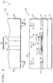
- FIG. 1 shows an enlarged simplified diagrammatic partial cross-sectional illustration of an optoelectronic interface module 100.
- optical connector 101 illustrated in cross-sectional view reveals an optical fiber 103 having a core region 104 and a cladding region 107, a body 108, and alignment devices 109.
- optoelectronic device 102 illustrated in cross-sectional view, reveals a molded optical portion 112, an optical surface 120, a photonic device 114, electronic tracings 115, an interconnect substrate 116, and alignment devices 117.
- FIG. 1 is a partial cross-sectional view and that optoelectronic interface module 100 can extend not only into and out of the drawing but also laterally across the drawing.
- optical fiber 103 and a single photonic device 114 are shown in FIG. 1, it should be understood that arrays of optical fibers, lens devices, and photonic devices are capable of being present in optoelectronic interface module 100.
- a novel combination of elements and processes are described that allow for accurate and efficient interconnection or coupling of optical fiber 103 to a working portion 118 of photonic device 114 through optical portion 112.
- interconnect substrate 116 is capable of being any suitable well-known interconnect substrate, such as a printed circuit board, a ceramic interconnect substrate, a printed wire board, or the like.
- interconnect substrate 116 provides a surface 105 having a plurality of electrical conductive pathways or electrical tracings, represented by electrical tracings 115, that interconnect a variety of electrical components (not shown), such as integrated circuits, resistors, capacitors, and the like to members 121 and photonic device 114, thereby electrically coupling the variety of electrical components to photonic device 114.
- Members 121 are capable of being any suitable input and output apparatus, such as lead frame members, wire bond connections, electrically conductive bumps, or the like.
- lead frame members are used to input and output electrical signals to and from optoelectronic device 102.
- lead frame members are electrically and mechanically coupled to electrical tracing 115 and subsequently overmolded, thereby securing members 121 and electrical tracings 115.
- members 121 are operably coupled to electrical tracings 115, thereby enabling electrical signals to be inputted and outputted through electrical tracings 115.
- Photonic device 114 is capable of being either a photo-transmitter or a photo-receiver that either emits light or receives light, respectively, as indicated by arrows 119.
- the photo-transmitter is capable of being any suitable light emitting device, such as a light emitting diode (LED), a vertical cavity surface emitting laser (VCSEL), or the like.
- photonic device 114 is capable of being any suitable light receiving device, such as a photodiode, a p-i-n photodiode, or the like.
- photonic device 114 when photonic device 114 is a photo-transmitter, and when photonic device 114 is a photo-receiver, photonic device 114 is either a vertical cavity surface emitting laser (VCSEL) or a p-i-n photodiode, respectively.
- VCSEL vertical cavity surface emitting laser
- photonic device 114 is made separately and subsequently electrically and mechanically joined to electrical tracings 115 through contacts 106 by any suitable method, such as manually, semi-automatically, or fully automatically.
- photonic device 114 is joined or mounted to electrical tracings 115 using an automatic system such as a robotic arm (not shown), thereby ensuring precise and accurate placement or mounting of photonic device 114 on tracings 115.
- molded optical portion 112 is made utilizing the teachings of U. S. Patent having U. S. Patent No. 5,265,184 issued November 23, 1993, that bears serial number 07/889,335, titled MOLDED WAVEGUIDE AND METHOD OF MAKING SAME, and was filed on May 28, 1992.
- molded optical portion 112 is made of any suitable optical material such as plastics, epoxies, polymers, or the like.
- prepared interconnect substrate 116 having photonic device 114 mounted thereon and members 121 operably coupled to electrical tracings 115, is placed into a molding system (not shown) and overmolded with molded optical portion 112, thereby encapsulating photonic device 114.
- molded optical portion 112 is formed or molded with optical surface 120 having a distance or a height 122 between surface 120 and working portion 118, represented by arrow 122.
- optical surface 120 is capable of being polished so as to make optical surface 120 more transparent, thereby increasing the transmission of light 119 through optical surface 120.
- optical surface 120 is capable of being polished or lapped to remove a portion of optical portion 112 of optical surface 120 so as to adjust the distance or the height 122 between optical surface 120 and working portion 118 of photonic device 114.
- optical portion 112 Materials used for optical portion 112 are optically clear with refractive indexes that are similar to refractive indexes of optical fiber 103, thereby allowing light 119 to pass through optical surface 120.
- refractive index of optical portion 112 is capable of including the range of refractive indexes of optical fiber 103, in a preferred embodiment of the present invention, refractive index of optical portion 112 is similar or matches the refractive index of that of core region 104.
- alignment devices 117 are made by any suitable method, such as molding, milling, or the like. However, in a preferred embodiment of the present invention, alignment devices 117 are molded simultaneously with optical portion 112, thereby providing accurate and precise alignment or placement of alignment devices 117 in relation to each other.
- conductive tracks 115 are made by any suitable well-known method in the art.
- the electrical signals are then passed through conductive bumps 110 that are made by any suitable method well known in the art, such as solder bumps, gold bumps, conductive epoxy bumps, or the like.
- gold bumps are used to provide a secure mechanical and electrical connection between electronic tracings 115 and photonic device 114.
- Optical connector 101 is made such that optical fiber 103 is held in a fixed position in relation to alignment devices 109, thereby providing a spatial orientation between core region 104 and alignment devices 109. Further, alignment devices 109 are positioned such that alignment devices 109 are capable of engaging alignment devices 117 of molded optical portion 112. In a preferred embodiment of the present invention, alignment devices 109 are detachably engaged with alignment devices 117 of molded optical portion 112, thereby aligning core region 104 to working portion 118 of photonic device 114. In the present invention, alignment of both core region 104 of optical fiber 103 and alignment of photonic device 114 are substantially relaxed, thereby providing a more manufacturable optoelectronic interface device 100 that does not require active alignment.
- FIG. 2 a highly enlarged simplified diagrammatic partial cross-sectional portion of optoelectronic interface module 100 is illustrated. It should be understood that features having similar or identical functions as illustrated in FIG. 1 will retain their original identifying numerals. As illustrated in FIG. 2, optical connector 101 is mated to optoelectronic device 102, thereby bring core region 104 in alignment with working portion 118 of photonic device 114 and optically coupling working portion 118 and core region 104.
- a distance or a height 122 is determined. Determination of distance or height 122 is achieved by solving the following mathematical inequality: wher e h is equal to distance or height 122 between surface 120 and working portion 118, where ⁇ 2 c (represented by arc 201 and 204) is equal to a critical angle or an acceptance angle, where d is equal to a width or a distance 202 of working portion 118 of photonic device 114, and where x is equal to one half of a desired spot size, represented by arrow 203 on optical surface 120.
- Acceptance angle or critical angle ⁇ 2 c is determined by solving the following mathematical inequality:
- Refractive indexes of core region 104, cladding region 107, and optical portion 112 are well-known material constants that are identified as n 3, n 2, and n 4 respectively.
- Solving for ⁇ 2 c results in determination of acceptance angle ⁇ 2 c , represented by arcs 201 and 204.
- Acceptance angle ⁇ 2 c determines an angle in which light is capable of being coupled between working portion 118 and core region 104. It should be understood that angle ⁇ 2 c represents an acceptance cone 210 that is defined by points 211, 212, 213, and 214 that rotate about an optical axis 215.
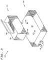
- FIG. 3 is an enlarged perspective view of an optoelectronic interconnect module 300.
- Optoelectronic interface module 300 includes optical connector 301 and optoelectronic interface device 302.
- optical connector 301 is made having a plurality of optical fibers (not shown) formed in an optical cable 308 that are held or fixed and positioned by a body 304 in such a manner that a plurality of core regions (not shown) of the plurality of optical fibers are exposed so as to be able to be operably coupled to photonic devices (not shown) in optoelectronic interface device 302.
- optical connector 301 is made with alignment devices 306 (only one is shown), thereby fixing spatial orientation of the plurality of core regions in relation to body 304. Insertion of alignment devices 306 into molded optical devices 309 aligns the plurality of core regions to the plurality of working portion of the plurality of photonic devices in optoelectronic interface device 302.
- Optoelectronic interface device 302 is made in a similar manner as has been described hereinabove. Engagement of alignment devices 306 with alignment devices 309 aligns the plurality of core regions in fiber optic cable 308 with the plurality of photonic devices in optoelectronic interface device 302 such that the plurality of core regions are operably or optically engaged to the plurality of photonic devices so to pass light thought surface 307 and into and out of optoelectronic interface device 302. Additionally, output members 118 are seen extending from optoelectronic interface device 302. These output members 118 are then capable of being further electrically interconnected to other electronic components or systems, such as printed circuit boards, computer boards, or the like.
- the optoelectronic interface device incorporates an optical portion that encapsulates a photonic device such that optical fibers in the optical connector and the working portion of the photonic device are operably coupled. Further, use of the optoelectronic interface device relaxes alignment tolerances that results in a cost effective method of manufacturing. Additionally, the method of making the optoelectronic interface device allows for the incorporation of standard electronic components with photonic devices in a highly manufacturable process.
Landscapes
- Physics & Mathematics (AREA)
- General Physics & Mathematics (AREA)
- Optics & Photonics (AREA)
- Optical Couplings Of Light Guides (AREA)
- Led Device Packages (AREA)
- Light Receiving Elements (AREA)
Applications Claiming Priority (2)
| Application Number | Priority Date | Filing Date | Title |
|---|---|---|---|
| US9545393A | 1993-07-19 | 1993-07-19 | |
| US95453 | 1993-07-19 |
Publications (3)
| Publication Number | Publication Date |
|---|---|
| EP0635741A2 true EP0635741A2 (de) | 1995-01-25 |
| EP0635741A3 EP0635741A3 (de) | 1996-01-10 |
| EP0635741B1 EP0635741B1 (de) | 2002-11-13 |
Family
ID=22252103
Family Applications (1)
| Application Number | Title | Priority Date | Filing Date |
|---|---|---|---|
| EP94109901A Expired - Lifetime EP0635741B1 (de) | 1993-07-19 | 1994-06-27 | Optoelektronische Überbrückung und Verfahren zu ihrer Herstellung |
Country Status (4)
| Country | Link |
|---|---|
| EP (1) | EP0635741B1 (de) |
| JP (1) | JPH0772355A (de) |
| KR (1) | KR950003844A (de) |
| DE (1) | DE69431696T2 (de) |
Cited By (5)
| Publication number | Priority date | Publication date | Assignee | Title |
|---|---|---|---|---|
| WO1996013069A1 (en) * | 1994-10-19 | 1996-05-02 | Telefonaktiebolaget Lm Ericsson | Optocomponent capsule having an optical interface |
| GB2333854A (en) * | 1998-01-31 | 1999-08-04 | Mitel Semiconductor Ab | Alignment of an optical member and an optical housing in an optical assembly |
| WO1999050700A1 (en) * | 1998-03-31 | 1999-10-07 | Honeywell Inc. | Chip-to-interface alignment |
| US8419295B2 (en) | 2007-01-26 | 2013-04-16 | Japan Aviation Electronics Industry, Limited | Photoelectric conversion/connection device |
| WO2015042225A2 (en) | 2013-09-18 | 2015-03-26 | Fci Asia Pte. Ltd | Optoelectrical connector system |
Family Cites Families (6)
| Publication number | Priority date | Publication date | Assignee | Title |
|---|---|---|---|---|
| JPS4910058A (de) * | 1972-03-30 | 1974-01-29 | ||
| EP0010352A1 (de) * | 1978-10-16 | 1980-04-30 | Motorola, Inc. | Opto-elektronische Halbleitervorrichtung |
| JPS55138891A (en) * | 1979-04-18 | 1980-10-30 | Fujitsu Ltd | Light semiconductor device |
| DE3172553D1 (en) * | 1980-11-28 | 1985-11-07 | Toshiba Kk | Method for manufacturing a module for a fiber optic link |
| DE3508627A1 (de) * | 1985-03-11 | 1986-09-11 | Siemens AG, 1000 Berlin und 8000 München | Vorrichtung zur ankopplung einer lichtwellenleiterfaser |
| US4995695A (en) * | 1989-08-17 | 1991-02-26 | At&T Bell Laboratories | Optical assembly comprising optical fiber coupling means |
-
1994
- 1994-06-27 EP EP94109901A patent/EP0635741B1/de not_active Expired - Lifetime
- 1994-06-27 DE DE69431696T patent/DE69431696T2/de not_active Expired - Fee Related
- 1994-07-13 JP JP6183015A patent/JPH0772355A/ja active Pending
- 1994-07-15 KR KR1019940017048A patent/KR950003844A/ko not_active Withdrawn
Cited By (8)
| Publication number | Priority date | Publication date | Assignee | Title |
|---|---|---|---|---|
| WO1996013069A1 (en) * | 1994-10-19 | 1996-05-02 | Telefonaktiebolaget Lm Ericsson | Optocomponent capsule having an optical interface |
| US5985185A (en) * | 1994-10-19 | 1999-11-16 | Telefonaktiebolaget Lm Ericsson | Optocomponent capsule having an optical interface |
| GB2333854A (en) * | 1998-01-31 | 1999-08-04 | Mitel Semiconductor Ab | Alignment of an optical member and an optical housing in an optical assembly |
| GB2333854B (en) * | 1998-01-31 | 2002-07-31 | Mitel Semiconductor Ab | System and method for aligning optical components |
| WO1999050700A1 (en) * | 1998-03-31 | 1999-10-07 | Honeywell Inc. | Chip-to-interface alignment |
| US6095697A (en) * | 1998-03-31 | 2000-08-01 | Honeywell International Inc. | Chip-to-interface alignment |
| US8419295B2 (en) | 2007-01-26 | 2013-04-16 | Japan Aviation Electronics Industry, Limited | Photoelectric conversion/connection device |
| WO2015042225A2 (en) | 2013-09-18 | 2015-03-26 | Fci Asia Pte. Ltd | Optoelectrical connector system |
Also Published As
| Publication number | Publication date |
|---|---|
| KR950003844A (ko) | 1995-02-17 |
| DE69431696T2 (de) | 2003-04-03 |
| DE69431696D1 (de) | 2002-12-19 |
| EP0635741B1 (de) | 2002-11-13 |
| JPH0772355A (ja) | 1995-03-17 |
| EP0635741A3 (de) | 1996-01-10 |
Similar Documents
| Publication | Publication Date | Title |
|---|---|---|
| US5428704A (en) | Optoelectronic interface and method of making | |
| US5369529A (en) | Reflective optoelectronic interface device and method of making | |
| DE102012200254B4 (de) | Optische Verbindungssysteme mit Stecker, welcher eine optische Biegung hat, und Benutzungsverfahren | |
| US5309537A (en) | Optoelectronic coupling device and method of making | |
| US5337391A (en) | Optoelectronic sub-module and method of making same | |
| US6203212B1 (en) | Optical subassembly for use in fiber optic data transmission and reception | |
| US7263256B2 (en) | Optical connection block, optical module, and optical axis alignment method using the same | |
| JP3628039B2 (ja) | 光結合素子およびその製造方法 | |
| US8412052B2 (en) | Surface mount (SMT) connector for VCSEL and photodiode arrays | |
| EP0613032B1 (de) | Faseroptische Kopplungseinrichtung | |
| US11092762B2 (en) | Surface mount packaging for single mode electro-optical module | |
| CN100516954C (zh) | 利用单个光纤光缆的双向光收发器模块 | |
| EP3163342A1 (de) | Fotoelektrische umwandlungsanordnung | |
| US7333683B2 (en) | Structure and method for mounting LSI package onto photoelectric wiring board, information processing apparatus, optical interface, and photoelectric wiring board | |
| US5522002A (en) | Method for making optical interface unit with detachable photonic device | |
| US5539200A (en) | Integrated optoelectronic substrate | |
| US5511138A (en) | Interlocking waveguide and method of making | |
| US5384873A (en) | Optical interface unit and method of making | |
| EP0635741B1 (de) | Optoelektronische Überbrückung und Verfahren zu ihrer Herstellung | |
| US20050220404A1 (en) | Optical interconnect module, and ferrule comprising same | |
| GB2416941A (en) | Passive alignment and coupling of an optical fibre with an optoelectonic device using a dual lens arrangement | |
| US20070104423A1 (en) | Z-axis alignment of an optoelectronic component using a spacer tool | |
| JPH0756062A (ja) | 光電インターフェースとその製造方法 |
Legal Events
| Date | Code | Title | Description |
|---|---|---|---|
| PUAI | Public reference made under article 153(3) epc to a published international application that has entered the european phase |
Free format text: ORIGINAL CODE: 0009012 |
|
| AK | Designated contracting states |
Kind code of ref document: A2 Designated state(s): DE FR GB |
|
| PUAL | Search report despatched |
Free format text: ORIGINAL CODE: 0009013 |
|
| AK | Designated contracting states |
Kind code of ref document: A3 Designated state(s): DE FR GB |
|
| 17P | Request for examination filed |
Effective date: 19960710 |
|
| 17Q | First examination report despatched |
Effective date: 19990922 |
|
| GRAG | Despatch of communication of intention to grant |
Free format text: ORIGINAL CODE: EPIDOS AGRA |
|
| GRAG | Despatch of communication of intention to grant |
Free format text: ORIGINAL CODE: EPIDOS AGRA |
|
| GRAH | Despatch of communication of intention to grant a patent |
Free format text: ORIGINAL CODE: EPIDOS IGRA |
|
| GRAH | Despatch of communication of intention to grant a patent |
Free format text: ORIGINAL CODE: EPIDOS IGRA |
|
| GRAA | (expected) grant |
Free format text: ORIGINAL CODE: 0009210 |
|
| AK | Designated contracting states |
Kind code of ref document: B1 Designated state(s): DE FR GB |
|
| REG | Reference to a national code |
Ref country code: GB Ref legal event code: FG4D |
|
| REF | Corresponds to: |
Ref document number: 69431696 Country of ref document: DE Date of ref document: 20021219 |
|
| ET | Fr: translation filed | ||
| PLBE | No opposition filed within time limit |
Free format text: ORIGINAL CODE: 0009261 |
|
| STAA | Information on the status of an ep patent application or granted ep patent |
Free format text: STATUS: NO OPPOSITION FILED WITHIN TIME LIMIT |
|
| 26N | No opposition filed |
Effective date: 20030814 |
|
| PGFP | Annual fee paid to national office [announced via postgrant information from national office to epo] |
Ref country code: GB Payment date: 20050506 Year of fee payment: 12 |
|
| PGFP | Annual fee paid to national office [announced via postgrant information from national office to epo] |
Ref country code: FR Payment date: 20050602 Year of fee payment: 12 |
|
| PGFP | Annual fee paid to national office [announced via postgrant information from national office to epo] |
Ref country code: DE Payment date: 20050630 Year of fee payment: 12 |
|
| PG25 | Lapsed in a contracting state [announced via postgrant information from national office to epo] |
Ref country code: GB Free format text: LAPSE BECAUSE OF NON-PAYMENT OF DUE FEES Effective date: 20060627 |
|
| PG25 | Lapsed in a contracting state [announced via postgrant information from national office to epo] |
Ref country code: DE Free format text: LAPSE BECAUSE OF NON-PAYMENT OF DUE FEES Effective date: 20070103 |
|
| GBPC | Gb: european patent ceased through non-payment of renewal fee |
Effective date: 20060627 |
|
| REG | Reference to a national code |
Ref country code: FR Ref legal event code: ST Effective date: 20070228 |
|
| PG25 | Lapsed in a contracting state [announced via postgrant information from national office to epo] |
Ref country code: FR Free format text: LAPSE BECAUSE OF NON-PAYMENT OF DUE FEES Effective date: 20060630 |