EP0630084A1 - Semiconductor laser - Google Patents
Semiconductor laser Download PDFInfo
- Publication number
- EP0630084A1 EP0630084A1 EP94109205A EP94109205A EP0630084A1 EP 0630084 A1 EP0630084 A1 EP 0630084A1 EP 94109205 A EP94109205 A EP 94109205A EP 94109205 A EP94109205 A EP 94109205A EP 0630084 A1 EP0630084 A1 EP 0630084A1
- Authority
- EP
- European Patent Office
- Prior art keywords
- layer
- cladding layer
- current confinement
- semiconductor laser
- cladding
- Prior art date
- Legal status (The legal status is an assumption and is not a legal conclusion. Google has not performed a legal analysis and makes no representation as to the accuracy of the status listed.)
- Granted
Links
Images


Classifications
-
- H—ELECTRICITY
- H01—ELECTRIC ELEMENTS
- H01S—DEVICES USING THE PROCESS OF LIGHT AMPLIFICATION BY STIMULATED EMISSION OF RADIATION [LASER] TO AMPLIFY OR GENERATE LIGHT; DEVICES USING STIMULATED EMISSION OF ELECTROMAGNETIC RADIATION IN WAVE RANGES OTHER THAN OPTICAL
- H01S5/00—Semiconductor lasers
- H01S5/30—Structure or shape of the active region; Materials used for the active region
- H01S5/32—Structure or shape of the active region; Materials used for the active region comprising PN junctions, e.g. hetero- or double- heterostructures
- H01S5/327—Structure or shape of the active region; Materials used for the active region comprising PN junctions, e.g. hetero- or double- heterostructures in AIIBVI compounds, e.g. ZnCdSe-laser
-
- H—ELECTRICITY
- H01—ELECTRIC ELEMENTS
- H01S—DEVICES USING THE PROCESS OF LIGHT AMPLIFICATION BY STIMULATED EMISSION OF RADIATION [LASER] TO AMPLIFY OR GENERATE LIGHT; DEVICES USING STIMULATED EMISSION OF ELECTROMAGNETIC RADIATION IN WAVE RANGES OTHER THAN OPTICAL
- H01S5/00—Semiconductor lasers
- H01S5/20—Structure or shape of the semiconductor body to guide the optical wave ; Confining structures perpendicular to the optical axis, e.g. index or gain guiding, stripe geometry, broad area lasers, gain tailoring, transverse or lateral reflectors, special cladding structures, MQW barrier reflection layers
- H01S5/22—Structure or shape of the semiconductor body to guide the optical wave ; Confining structures perpendicular to the optical axis, e.g. index or gain guiding, stripe geometry, broad area lasers, gain tailoring, transverse or lateral reflectors, special cladding structures, MQW barrier reflection layers having a ridge or stripe structure
- H01S5/2205—Structure or shape of the semiconductor body to guide the optical wave ; Confining structures perpendicular to the optical axis, e.g. index or gain guiding, stripe geometry, broad area lasers, gain tailoring, transverse or lateral reflectors, special cladding structures, MQW barrier reflection layers having a ridge or stripe structure comprising special burying or current confinement layers
- H01S5/2214—Structure or shape of the semiconductor body to guide the optical wave ; Confining structures perpendicular to the optical axis, e.g. index or gain guiding, stripe geometry, broad area lasers, gain tailoring, transverse or lateral reflectors, special cladding structures, MQW barrier reflection layers having a ridge or stripe structure comprising special burying or current confinement layers based on oxides or nitrides
-
- H—ELECTRICITY
- H01—ELECTRIC ELEMENTS
- H01S—DEVICES USING THE PROCESS OF LIGHT AMPLIFICATION BY STIMULATED EMISSION OF RADIATION [LASER] TO AMPLIFY OR GENERATE LIGHT; DEVICES USING STIMULATED EMISSION OF ELECTROMAGNETIC RADIATION IN WAVE RANGES OTHER THAN OPTICAL
- H01S5/00—Semiconductor lasers
- H01S5/20—Structure or shape of the semiconductor body to guide the optical wave ; Confining structures perpendicular to the optical axis, e.g. index or gain guiding, stripe geometry, broad area lasers, gain tailoring, transverse or lateral reflectors, special cladding structures, MQW barrier reflection layers
- H01S5/22—Structure or shape of the semiconductor body to guide the optical wave ; Confining structures perpendicular to the optical axis, e.g. index or gain guiding, stripe geometry, broad area lasers, gain tailoring, transverse or lateral reflectors, special cladding structures, MQW barrier reflection layers having a ridge or stripe structure
- H01S5/223—Buried stripe structure
Landscapes
- Physics & Mathematics (AREA)
- Condensed Matter Physics & Semiconductors (AREA)
- General Physics & Mathematics (AREA)
- Electromagnetism (AREA)
- Optics & Photonics (AREA)
- Semiconductor Lasers (AREA)
Abstract
Description
- The present invention relates to a semiconductor laser and particularly to a semiconductor laser whose active layer is made of a II-VI group compound semiconductor material and a manufacturing method thereof.
- It is difficult to obtain a satisfactory ohmic contact at a p side in a semiconductor laser in which a II-VI group compound semiconductor material of ZnSe system or the like is used. Therefore, the prior art is encountered by such disadvantage that generation of heat at a contact portion causes deterioration of an electrode, rise in temperature of an element makes long-time operation difficult, or the like.
- Construction of the ZnSe system semiconductor laser as an example will be explained with reference to FIGS. 1A to 1C showing manufacturing processes thereof. In this case, first, as shown in FIG. 1A, a
first cladding layer 2 made of an n type ZnMgSSe or the like, anactive layer 3 made of an undoped ZnCdSe or the like, asecond cladding layer 4 made of a p type ZnMgSSe or the like, abuffer layer 5 made of a p type ZnSe or the like and further acontact layer 6 having a p type ZnSe/ZnTe superlattice structure are successively epitaxially grown on asubstrate 1 made of an n type GaAs or the like. Aphotoresist 10 is coated on thecontact layer 6 and then subjected to patterning by pattern exposure and development in a striped fashion so as to cover a region where a striped current path is to be formed. With using thephotoresist 10 as a resist mask, thecontact layer 6 is subjected to the patterning by chemical etching or the like so as to have a striped shape. At this time, until a part of each of thebuffer layers 5 at both sides of thecontact layer 6 is removed, the etching is performed. - Then, after the
photoresist 10 is removed and then apolyimide 11 is coated on the whole surface, as shown in FIG. 1B, only thecontact layer 6 is exposed by a proper photolithography technique. - Next, as shown in FIG. 1C, an
electrode 8 formed of a multilayer film of Pd/Pt/Au or the like is formed by vacuum evaporation or the like so as to completely cover thepolyimide 11 and thecontact layer 6.Reference numeral 9 represents an electrode which is made of In or the like and previously formed by the coating on a rear surface of thesubstrate 1, for example, or the like. - As described above, the
polyimide 11 blocks the current and the region sandwiched by thepolyimide 11 is set as the striped current path, thereby constructing a semiconductor laser of a gain waveguide type. - The
polyimide 11 has such advantages that it has excellent property in adhesion to ZnSe and a p side electrode, can be formed as a film by a process at a comparatively low temperature, and is prevented from damaging crystallinity of another portions. - However, the above-mentioned semiconductor laser of gain waveguide type has such disadvantage that since most injected current is concentrated on a portion just beneath an electrode having large contact resistance, it cannot be avoided that Joule heat generated around the electrode deteriorates the electrode portion and raise temperature of the whole of a laser element.
- There can be considered a countermeasure thereagainst such that the p side electrode is located at a lower portion of the element in order to suppress rise of temperature of the element and is mounted on a heat sink having very high thermal conductivity, while there is then the problem that since the
polyimide 11 is provided on a portion occupying a comparatively large area between the p side electrode and the cladding layer, the heat cannot be effectively exhausted. - According to the present invention, particularly in the II-VI group compound semiconductor laser of ZnSe system or the like, heat-radiation characteristic can be improved, and long-time operation thereof is made possible.
- A semiconductor laser according to the present invention comprises a first cladding layer of a first conductivity type on a substrate, an active layer laminated on the first cladding layer, a second cladding layer of a second conductivity type laminated on the active layer, and a current confinement layer on the second cladding layer, in which the first cladding layer, the active layer and the second cladding layer are made of a II-VI group compound semiconductor and the current confinement layer is made of a metal oxide whose thermal conductivity is equal to or larger than 0.01 cal/cm·s·°C.
- According to the present invention having the above-mentioned construction, a silicon layer is provided between the current confinement layer and an electrode.
- Further, according to the present invention having the above-mentioned construction, the current confinement layer is provided on an upper portion of a p type semiconductor layer.
-
- FIGS. 1A, 1B and 1C are manufacturing process diagrams of one example of a semiconductor laser;
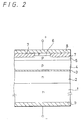
- FIG. 2 is a schematically enlarged and cross-sectional view of an embodiment according to the present invention;
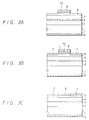
- FIGS. 3A, 3B and 3C are manufacturing process diagrams of the embodiment according to the present invention; and
- FIG. 4 is a schematically enlarged and cross-sectional view of another embodiment according to the present invention.
- Through study and research of the inventor of the present invention, it is found that as shown in FIG. 2 which is a schematically enlarged and cross-sectional view of one embodiment of the present invention, when a semiconductor laser whose active layer is made of II-VI group compound semiconductor is constructed, a metal oxide having satisfactory thermal conductivity in which its thermal conductivity at 100 °C is equal to or larger than 0.01 cal/cm·s·°C is used particularly as a material of a
current confinement layer 7 thereof to thereby obtain sufficient heat-radiation characteristic and enable an element to be operated for a long period of time. - A silicon layer is provided between the
current confinement layer 7 made of such metal oxide and anelectrode 8 thereon, whereby adhesion between thecurrent confinement layer 7 made of the metal oxide and theelectrode 8 can be improved and the peeling off or the like can be prevented from being caused to thereby provide a highly reliable semiconductor laser. - Such
current confinement layer 7, as shown in FIGS. 3A to 3C which show a manufacturing process of one example thereof, is formed in a self-alignment fashion with using aresist 10 on a striped current path as a mask, whereby positional displacement thereof relative to acontact layer 6 can be suppressed and reduction of the number of manufacturing processes and improvement of productivity can be achieved. - An embodiment according to the present invention will hereinafter be explained with reference to the accompanying drawings. This example is the case where a ZnSe system compound semiconductor laser is constructed on a GaAs substrate, and one example of a manufacturing method thereof will first be explained in detail with reference to FIGS. 3A to 3C.
- As shown in FIG. 3A,
reference numeral 1 represents a substrate made of an n type GaAs, for example, in which anelectrode 9 made of, for example, In or the like is coated as an n side electrode on a rear surface thereof and formed by the heating and the melting in the succeeding epitaxial growth process. On thesubstrate 1, afirst cladding layer 2 made of an n type ZnMgSSe or the like, anactive layer 3 made of undoped ZnCdSe or the like, asecond cladding layer 4 made of a p type ZnMgSSe or the like, abuffer layer 5 made of a p type ZnSe or the like and further acontact layer 6 having a p type ZnSe/ZnTe superlattice structure, for example, are successively epitaxially grown by an MOCVD (metal organic chemical vapor deposition), an MBE (molecular beam epitaxy) or the like. - Next, the
photoresist 10 is coated on thecontact layer 6 and then subjected to patterning by pattern exposure and development in a striped fashion so as to cover a region where a striped current path is to be formed. With using thephotoresist 10 as a resist mask, thecontact layer 6 is subjected to the patterning by chemical etching or the like so as to have a striped shape. At this time, until a part of each of thebuffer layers 5 at both sides of thecontact layer 6 is removed, the etching is performed. - Next, as shown in FIG. 3B, with the
photoresist 10 being kept left, thecurrent confinement layer 7 made of a metal oxide whose thermal conductivity at 100°C is equal to or larger than 0.01 cal/cm·s·°C, for example, Al₂O₃ whose thermal conductivity is 0.07 cal/cm·s·°C (a value at 100 °C, a value at 100 °C of the thermal conductivity will hereinafter be shown as a value of the thermal conductivity) is deposited by the vacuum evaporation or the like on the whole surface. - As shown in FIG. 3C, after the photoresist and the Al₂O₃ thereon are removed to expose the
contact layer 6, as shown in FIG. 2, theelectrode 8 formed of a multilayer film of Pd/Pt/Au or the like is formed on the whole surface by vacuum evaporation or the like. Thus, there is constructed a semiconductor laser of gain waveguide type in which a region surrounded by thecurrent confinement layer 7 made of the above-mentioned metal oxide is formed as a striped current path. - In this case, a photolithography process is required once, and the
current confinement layer 7 can be formed in self-alignment fashion simultaneously with the patterning of thecontact layer 6, so that positional displacement between thecontact layer 6 and thecurrent confinement layer 7 can be suppressed. - That is, when a polyimide is used as the current confinement layer on the p type semiconductor layer in the prior art, the photolithography is required twice as explained in the above FIGS. 1A to 1C which show a manufacturing process thereof, while as described above, according to the present invention, the number of photolithography processes can be reduced to one, hence the number of manufacturing processes can be reduced, and further productivity can be improved.
- A
silicon layer 12 is provided between thecurrent confinement 7 and theelectrode 8 as shown in FIG. 4, whereby adhesion at this portion can be made sufficiently large. A forming method of thesilicon layer 12 proceeds in such a manner that in the above-mentioned process shown in FIG. 3B, for example, after thecurrent confinement layer 7 made of the metal oxide is deposited by the vacuum evaporation, thesilicon layer 12 is deposited by the vacuum evaporation on the whole surface and then can be formed in self-alignment fashion by similarly removing the photoresist. The silicon is high in the thermal conductivity as compared with the metal oxide such as Al₂O₃ or the like, so that drastic deterioration of the heat-radiation characteristic can be avoided as compared with the case where only the metal oxide is used. - Besides the above-mentioned Al₂O₃, it is sufficient for a material of the
current confinement layer 7 that the thermal conductivity is equal to or larger than 0.01 cal/cm·s·°C. As a material which can have property of self-alignment, that is, can be deposited by the vacuum evaporation, there can be used a material such as MgO whose thermal conductivity is 0.09 cal/cm·s·°C, BeO whose thermal conductivity is 0.53 cal/cm·s·°C, or the like. - The thermal conductivity of the polyimide is within the range from 0.0003 to 0.0005 cal/cm·s·°C. An insulating material whose thermal conductivity is higher than that of the polyimide is SiO₂, for example, whose thermal conductivity is 0.005 cal/cm·s·°C. When SiO₂ is employed as the current confinement layer of the semiconductor laser having the active layer formed of the above-mentioned II-VI group compound semiconductor, sufficient heat-radiation characteristic could not be obtained. Accordingly, in the present invention, the metal oxide whose thermal conductivity is equal to or larger than 0.01 cal/cm·s·°C is used.
- As described above, according to the present invention, in the semiconductor laser made of II-VI group compound semiconductor of ZnSe system or the like, the heat-radiation characteristic thereof can be improved and the longtime operation thereof is made possible.
- The number of the lithographic processes in the manufacture thereof can be reduced to one, whereby the number of the manufacturing processes can be reduced and the productivity thereof can be improved.
- Further, the silicon layer is provided between the current confinement layer and the electrode, whereby the adhesion property thereof can be improved and hence more reliable semiconductor laser can be provided.
- Having described preferred embodiments of the invention with reference to the drawings, it is to be understood that the invention is not limited to that precise embodiments and that various changes and modifications can be effected therein by one skilled in the art without departing from the spirit or scope of the novel concepts of the invention as defined in the appended claims.
Claims (4)
- A semiconductor laser comprising:
a semiconductor substrate;
a first cladding layer of a first conductive type disposed on said semiconductor substrate;
an active layer disposed on said first cladding layer,
a second cladding layer of a second conductivity type disposed on said active layer; and
a current confinement layer on said second cladding layer;
wherein said first cladding layer, said second cladding layer and said active layer are made of II-VI group compound and said current confinement layer is made of a metal oxide having a thermal conductivity which is not less than 0.01 cal / cm·s·°C. - The semiconductor laser according to Claim 1, wherein a silicon layer is provided between said current confinement layer and an electrode.
- The semiconductor laser according to Claim 1, wherein said current confinement layer is provided on an upper portion of a p type semiconductor layer.
- A semiconductor laser comprising:
a semiconductor substrate;
a first cladding layer of a first conductive type disposed on said semiconductor substrate;
an active layer disposed on said first cladding layer;
a second cladding layer of a second conductivity type disposed on said active layer; and
a current confinement layer on said second cladding layer;
wherein said first cladding layer, said second cladding layer and said active layer are made of II-VI group compound and said current confinement layer is made of Al₂O₃, MgO or BeO.
Applications Claiming Priority (2)
| Application Number | Priority Date | Filing Date | Title |
|---|---|---|---|
| JP14795793A JP3453787B2 (en) | 1993-06-18 | 1993-06-18 | Semiconductor laser and manufacturing method thereof |
| JP147957/93 | 1993-06-18 |
Publications (2)
| Publication Number | Publication Date |
|---|---|
| EP0630084A1 true EP0630084A1 (en) | 1994-12-21 |
| EP0630084B1 EP0630084B1 (en) | 1997-03-19 |
Family
ID=15441912
Family Applications (1)
| Application Number | Title | Priority Date | Filing Date |
|---|---|---|---|
| EP94109205A Expired - Lifetime EP0630084B1 (en) | 1993-06-18 | 1994-06-15 | Semiconductor laser |
Country Status (6)
| Country | Link |
|---|---|
| US (1) | US5432810A (en) |
| EP (1) | EP0630084B1 (en) |
| JP (1) | JP3453787B2 (en) |
| KR (1) | KR100277398B1 (en) |
| DE (1) | DE69402115T2 (en) |
| TW (1) | TW274646B (en) |
Families Citing this family (4)
| Publication number | Priority date | Publication date | Assignee | Title |
|---|---|---|---|---|
| KR100303279B1 (en) * | 1994-08-27 | 2001-12-01 | 윤종용 | Semiconductor laser diode and manufacturing method therefor |
| JP3193976B2 (en) * | 1996-03-27 | 2001-07-30 | 松下電器産業株式会社 | High voltage noise filter and magnetron device |
| US5732103A (en) * | 1996-12-09 | 1998-03-24 | Motorola, Inc. | Long wavelength VCSEL |
| JP2006012899A (en) * | 2004-06-22 | 2006-01-12 | Sharp Corp | Semiconductor laser device and its manufacturing method |
Citations (3)
| Publication number | Priority date | Publication date | Assignee | Title |
|---|---|---|---|---|
| US5029175A (en) * | 1988-12-08 | 1991-07-02 | Matsushita Electric Industrial Co., Ltd. | Semiconductor laser |
| JPH03237785A (en) * | 1990-02-15 | 1991-10-23 | Omron Corp | Semiconductor light emitting element and manufacture thereof |
| WO1992021170A2 (en) * | 1991-05-15 | 1992-11-26 | Minnesota Mining And Manufacturing Company | Blue-green laser diode |
Family Cites Families (3)
| Publication number | Priority date | Publication date | Assignee | Title |
|---|---|---|---|---|
| US4955031A (en) * | 1988-07-12 | 1990-09-04 | University Of Connecticut | Metal insulator semiconductor heterostructure lasers |
| JPH05275803A (en) * | 1992-03-27 | 1993-10-22 | Tdk Corp | Semiconductor laser |
| JPH0621572A (en) * | 1992-07-02 | 1994-01-28 | Nec Corp | Semiconductor laser |
-
1993
- 1993-06-18 JP JP14795793A patent/JP3453787B2/en not_active Expired - Lifetime
-
1994
- 1994-06-15 EP EP94109205A patent/EP0630084B1/en not_active Expired - Lifetime
- 1994-06-15 TW TW083105419A patent/TW274646B/zh active
- 1994-06-15 DE DE69402115T patent/DE69402115T2/en not_active Expired - Fee Related
- 1994-06-16 US US08/261,195 patent/US5432810A/en not_active Expired - Fee Related
- 1994-06-16 KR KR1019940013559A patent/KR100277398B1/en not_active IP Right Cessation
Patent Citations (3)
| Publication number | Priority date | Publication date | Assignee | Title |
|---|---|---|---|---|
| US5029175A (en) * | 1988-12-08 | 1991-07-02 | Matsushita Electric Industrial Co., Ltd. | Semiconductor laser |
| JPH03237785A (en) * | 1990-02-15 | 1991-10-23 | Omron Corp | Semiconductor light emitting element and manufacture thereof |
| WO1992021170A2 (en) * | 1991-05-15 | 1992-11-26 | Minnesota Mining And Manufacturing Company | Blue-green laser diode |
Non-Patent Citations (3)
| Title |
|---|
| ANONYMOUS; NO.34603: "Contact Structure for II-VI Semiconductor Lasers", RESEARCH DISCLOSURE, no. 346, February 1993 (1993-02-01), EMSWORTH,GB, pages 81, XP000358754 * |
| F. HIEI ET AL.: "Ohmic Contacts to p-Type ZnSe Using ZnTe/ZnSe Multiquantum Wells", ELECTRONICS LETTERS, vol. 29, no. 10, 13 May 1993 (1993-05-13), STEVENAGE, GB, pages 878 - 879, XP000367649 * |
| PATENT ABSTRACTS OF JAPAN vol. 16, no. 22 (E - 1156) 20 January 1992 (1992-01-20) * |
Also Published As
| Publication number | Publication date |
|---|---|
| EP0630084B1 (en) | 1997-03-19 |
| TW274646B (en) | 1996-04-21 |
| JP3453787B2 (en) | 2003-10-06 |
| DE69402115T2 (en) | 1997-11-13 |
| US5432810A (en) | 1995-07-11 |
| DE69402115D1 (en) | 1997-04-24 |
| KR100277398B1 (en) | 2001-02-01 |
| JPH077220A (en) | 1995-01-10 |
Similar Documents
| Publication | Publication Date | Title |
|---|---|---|
| US5701321A (en) | Semiconductor laser producing short wavelength light | |
| EP0963017B1 (en) | Semiconductor emission element and method of manufacturing same | |
| EP0630084B1 (en) | Semiconductor laser | |
| JPH10335696A (en) | Light emitting diode array | |
| US20020075925A1 (en) | Growing a low defect gallium nitride based semiconductor | |
| JP2000299528A (en) | Semiconductor laser and manufacture thereof | |
| KR100323237B1 (en) | Light Emitting Semiconductor Device to Suppress Variation of Driving Circuit | |
| US5270245A (en) | Method of forming a light emitting diode | |
| JP2005505133A (en) | Method of manufacturing a semiconductor device based on nitride-compound semiconductor | |
| EP0205338B1 (en) | Semiconductor laser device | |
| US5805628A (en) | Semiconductor laser | |
| JPS5820153B2 (en) | Manufacturing method of compound semiconductor light emitting device | |
| JP4221818B2 (en) | Method for manufacturing optical semiconductor element | |
| JPH11340569A (en) | Formation of electrode of semiconductor element and its structure | |
| US5887011A (en) | Semiconductor laser | |
| EP0133996A2 (en) | Semiconductor laser | |
| US5196369A (en) | Method of producing a light emitting diode array device | |
| JPH1041583A (en) | Semiconductor light-emitting device | |
| JP3505913B2 (en) | Method for manufacturing semiconductor light emitting device | |
| JP2003008055A (en) | Method of manufacturing semiconductor light-emitting element | |
| JPH0983015A (en) | Fabrication of monolithic light emitting diode array | |
| JPH10209559A (en) | Semiconductor light emitting element and manufacture thereof | |
| JP3075824B2 (en) | Surface emitting semiconductor laser device and method of manufacturing the same | |
| JP2002094169A (en) | Nitride semiconductor laser device and its manufacturing method | |
| JPH11163408A (en) | Light-emitting diode array |
Legal Events
| Date | Code | Title | Description |
|---|---|---|---|
| PUAI | Public reference made under article 153(3) epc to a published international application that has entered the european phase |
Free format text: ORIGINAL CODE: 0009012 |
|
| AK | Designated contracting states |
Kind code of ref document: A1 Designated state(s): DE FR GB |
|
| 17P | Request for examination filed |
Effective date: 19950519 |
|
| 17Q | First examination report despatched |
Effective date: 19951018 |
|
| GRAG | Despatch of communication of intention to grant |
Free format text: ORIGINAL CODE: EPIDOS AGRA |
|
| GRAH | Despatch of communication of intention to grant a patent |
Free format text: ORIGINAL CODE: EPIDOS IGRA |
|
| GRAH | Despatch of communication of intention to grant a patent |
Free format text: ORIGINAL CODE: EPIDOS IGRA |
|
| GRAA | (expected) grant |
Free format text: ORIGINAL CODE: 0009210 |
|
| AK | Designated contracting states |
Kind code of ref document: B1 Designated state(s): DE FR GB |
|
| REF | Corresponds to: |
Ref document number: 69402115 Country of ref document: DE Date of ref document: 19970424 |
|
| ET | Fr: translation filed | ||
| PLBE | No opposition filed within time limit |
Free format text: ORIGINAL CODE: 0009261 |
|
| STAA | Information on the status of an ep patent application or granted ep patent |
Free format text: STATUS: NO OPPOSITION FILED WITHIN TIME LIMIT |
|
| 26N | No opposition filed | ||
| PGFP | Annual fee paid to national office [announced via postgrant information from national office to epo] |
Ref country code: FR Payment date: 20010611 Year of fee payment: 8 Ref country code: DE Payment date: 20010611 Year of fee payment: 8 |
|
| PGFP | Annual fee paid to national office [announced via postgrant information from national office to epo] |
Ref country code: GB Payment date: 20010613 Year of fee payment: 8 |
|
| REG | Reference to a national code |
Ref country code: GB Ref legal event code: IF02 |
|
| PG25 | Lapsed in a contracting state [announced via postgrant information from national office to epo] |
Ref country code: GB Free format text: LAPSE BECAUSE OF NON-PAYMENT OF DUE FEES Effective date: 20020615 |
|
| PG25 | Lapsed in a contracting state [announced via postgrant information from national office to epo] |
Ref country code: DE Free format text: LAPSE BECAUSE OF NON-PAYMENT OF DUE FEES Effective date: 20030101 |
|
| GBPC | Gb: european patent ceased through non-payment of renewal fee |
Effective date: 20020615 |
|
| PG25 | Lapsed in a contracting state [announced via postgrant information from national office to epo] |
Ref country code: FR Free format text: LAPSE BECAUSE OF NON-PAYMENT OF DUE FEES Effective date: 20030228 |
|
| REG | Reference to a national code |
Ref country code: FR Ref legal event code: ST |