EP0627767B1 - Process for fabricating JFET transistors and capacitors - Google Patents
Process for fabricating JFET transistors and capacitors Download PDFInfo
- Publication number
- EP0627767B1 EP0627767B1 EP94112898A EP94112898A EP0627767B1 EP 0627767 B1 EP0627767 B1 EP 0627767B1 EP 94112898 A EP94112898 A EP 94112898A EP 94112898 A EP94112898 A EP 94112898A EP 0627767 B1 EP0627767 B1 EP 0627767B1
- Authority
- EP
- European Patent Office
- Prior art keywords
- region
- layer
- junction isolation
- forming
- jfet
- Prior art date
- Legal status (The legal status is an assumption and is not a legal conclusion. Google has not performed a legal analysis and makes no representation as to the accuracy of the status listed.)
- Expired - Lifetime
Links
- 238000000034 method Methods 0.000 title claims description 21
- 239000003990 capacitor Substances 0.000 title claims description 18
- 239000002019 doping agent Substances 0.000 claims description 28
- 239000000758 substrate Substances 0.000 claims description 25
- 238000002955 isolation Methods 0.000 claims description 22
- 239000004065 semiconductor Substances 0.000 claims description 9
- 229910052710 silicon Inorganic materials 0.000 claims description 6
- 239000010703 silicon Substances 0.000 claims description 6
- 230000005669 field effect Effects 0.000 claims description 4
- 239000012212 insulator Substances 0.000 claims 4
- VYPSYNLAJGMNEJ-UHFFFAOYSA-N Silicium dioxide Chemical compound O=[Si]=O VYPSYNLAJGMNEJ-UHFFFAOYSA-N 0.000 claims 2
- 235000012239 silicon dioxide Nutrition 0.000 claims 1
- 239000000377 silicon dioxide Substances 0.000 claims 1
- 238000009792 diffusion process Methods 0.000 description 15
- 238000004519 manufacturing process Methods 0.000 description 12
- 238000002513 implantation Methods 0.000 description 10
- 229910021420 polycrystalline silicon Inorganic materials 0.000 description 9
- 229920005591 polysilicon Polymers 0.000 description 8
- 230000015556 catabolic process Effects 0.000 description 7
- 229910052751 metal Inorganic materials 0.000 description 7
- 239000002184 metal Substances 0.000 description 7
- 150000004767 nitrides Chemical class 0.000 description 6
- XUIMIQQOPSSXEZ-UHFFFAOYSA-N Silicon Chemical compound [Si] XUIMIQQOPSSXEZ-UHFFFAOYSA-N 0.000 description 5
- 230000008021 deposition Effects 0.000 description 5
- 229920002120 photoresistant polymer Polymers 0.000 description 4
- 230000000873 masking effect Effects 0.000 description 3
- 230000003071 parasitic effect Effects 0.000 description 3
- ZOXJGFHDIHLPTG-UHFFFAOYSA-N Boron Chemical compound [B] ZOXJGFHDIHLPTG-UHFFFAOYSA-N 0.000 description 2
- 229910052787 antimony Inorganic materials 0.000 description 2
- WATWJIUSRGPENY-UHFFFAOYSA-N antimony atom Chemical group [Sb] WATWJIUSRGPENY-UHFFFAOYSA-N 0.000 description 2
- 230000015572 biosynthetic process Effects 0.000 description 2
- 229910052796 boron Inorganic materials 0.000 description 2
- 238000010276 construction Methods 0.000 description 2
- 230000005684 electric field Effects 0.000 description 2
- OAICVXFJPJFONN-UHFFFAOYSA-N Phosphorus Chemical compound [P] OAICVXFJPJFONN-UHFFFAOYSA-N 0.000 description 1
- 229910052782 aluminium Inorganic materials 0.000 description 1
- XAGFODPZIPBFFR-UHFFFAOYSA-N aluminium Chemical compound [Al] XAGFODPZIPBFFR-UHFFFAOYSA-N 0.000 description 1
- 239000007943 implant Substances 0.000 description 1
- 238000010348 incorporation Methods 0.000 description 1
- 239000000463 material Substances 0.000 description 1
- 238000004377 microelectronic Methods 0.000 description 1
- 230000003647 oxidation Effects 0.000 description 1
- 238000007254 oxidation reaction Methods 0.000 description 1
- 238000000059 patterning Methods 0.000 description 1
- 229910052698 phosphorus Inorganic materials 0.000 description 1
- 239000011574 phosphorus Substances 0.000 description 1
- 239000013589 supplement Substances 0.000 description 1
Images
Classifications
-
- H—ELECTRICITY
- H01—ELECTRIC ELEMENTS
- H01L—SEMICONDUCTOR DEVICES NOT COVERED BY CLASS H10
- H01L29/00—Semiconductor devices adapted for rectifying, amplifying, oscillating or switching, or capacitors or resistors with at least one potential-jump barrier or surface barrier, e.g. PN junction depletion layer or carrier concentration layer; Details of semiconductor bodies or of electrodes thereof ; Multistep manufacturing processes therefor
- H01L29/66—Types of semiconductor device ; Multistep manufacturing processes therefor
- H01L29/68—Types of semiconductor device ; Multistep manufacturing processes therefor controllable by only the electric current supplied, or only the electric potential applied, to an electrode which does not carry the current to be rectified, amplified or switched
- H01L29/70—Bipolar devices
-
- H—ELECTRICITY
- H01—ELECTRIC ELEMENTS
- H01L—SEMICONDUCTOR DEVICES NOT COVERED BY CLASS H10
- H01L27/00—Devices consisting of a plurality of semiconductor or other solid-state components formed in or on a common substrate
- H01L27/02—Devices consisting of a plurality of semiconductor or other solid-state components formed in or on a common substrate including semiconductor components specially adapted for rectifying, oscillating, amplifying or switching and having at least one potential-jump barrier or surface barrier; including integrated passive circuit elements with at least one potential-jump barrier or surface barrier
- H01L27/04—Devices consisting of a plurality of semiconductor or other solid-state components formed in or on a common substrate including semiconductor components specially adapted for rectifying, oscillating, amplifying or switching and having at least one potential-jump barrier or surface barrier; including integrated passive circuit elements with at least one potential-jump barrier or surface barrier the substrate being a semiconductor body
- H01L27/06—Devices consisting of a plurality of semiconductor or other solid-state components formed in or on a common substrate including semiconductor components specially adapted for rectifying, oscillating, amplifying or switching and having at least one potential-jump barrier or surface barrier; including integrated passive circuit elements with at least one potential-jump barrier or surface barrier the substrate being a semiconductor body including a plurality of individual components in a non-repetitive configuration
- H01L27/0611—Devices consisting of a plurality of semiconductor or other solid-state components formed in or on a common substrate including semiconductor components specially adapted for rectifying, oscillating, amplifying or switching and having at least one potential-jump barrier or surface barrier; including integrated passive circuit elements with at least one potential-jump barrier or surface barrier the substrate being a semiconductor body including a plurality of individual components in a non-repetitive configuration integrated circuits having a two-dimensional layout of components without a common active region
- H01L27/0617—Devices consisting of a plurality of semiconductor or other solid-state components formed in or on a common substrate including semiconductor components specially adapted for rectifying, oscillating, amplifying or switching and having at least one potential-jump barrier or surface barrier; including integrated passive circuit elements with at least one potential-jump barrier or surface barrier the substrate being a semiconductor body including a plurality of individual components in a non-repetitive configuration integrated circuits having a two-dimensional layout of components without a common active region comprising components of the field-effect type
- H01L27/0623—Devices consisting of a plurality of semiconductor or other solid-state components formed in or on a common substrate including semiconductor components specially adapted for rectifying, oscillating, amplifying or switching and having at least one potential-jump barrier or surface barrier; including integrated passive circuit elements with at least one potential-jump barrier or surface barrier the substrate being a semiconductor body including a plurality of individual components in a non-repetitive configuration integrated circuits having a two-dimensional layout of components without a common active region comprising components of the field-effect type in combination with bipolar transistors
-
- H—ELECTRICITY
- H01—ELECTRIC ELEMENTS
- H01L—SEMICONDUCTOR DEVICES NOT COVERED BY CLASS H10
- H01L21/00—Processes or apparatus adapted for the manufacture or treatment of semiconductor or solid state devices or of parts thereof
- H01L21/70—Manufacture or treatment of devices consisting of a plurality of solid state components formed in or on a common substrate or of parts thereof; Manufacture of integrated circuit devices or of parts thereof
- H01L21/71—Manufacture of specific parts of devices defined in group H01L21/70
- H01L21/76—Making of isolation regions between components
- H01L21/761—PN junctions
-
- H—ELECTRICITY
- H01—ELECTRIC ELEMENTS
- H01L—SEMICONDUCTOR DEVICES NOT COVERED BY CLASS H10
- H01L21/00—Processes or apparatus adapted for the manufacture or treatment of semiconductor or solid state devices or of parts thereof
- H01L21/70—Manufacture or treatment of devices consisting of a plurality of solid state components formed in or on a common substrate or of parts thereof; Manufacture of integrated circuit devices or of parts thereof
- H01L21/77—Manufacture or treatment of devices consisting of a plurality of solid state components or integrated circuits formed in, or on, a common substrate
- H01L21/78—Manufacture or treatment of devices consisting of a plurality of solid state components or integrated circuits formed in, or on, a common substrate with subsequent division of the substrate into plural individual devices
- H01L21/82—Manufacture or treatment of devices consisting of a plurality of solid state components or integrated circuits formed in, or on, a common substrate with subsequent division of the substrate into plural individual devices to produce devices, e.g. integrated circuits, each consisting of a plurality of components
- H01L21/822—Manufacture or treatment of devices consisting of a plurality of solid state components or integrated circuits formed in, or on, a common substrate with subsequent division of the substrate into plural individual devices to produce devices, e.g. integrated circuits, each consisting of a plurality of components the substrate being a semiconductor, using silicon technology
- H01L21/8248—Combination of bipolar and field-effect technology
Definitions
- This invention relates in general to the fabrication of different integrated circuit devices using a single semiconductor substrate, and more particularly to a process for simultaneously fabricating a junction field effect transistor (JFET) and a capacitor.
- JFET junction field effect transistor
- VPNP high-frequency isolated vertical PNP
- This isolated VPNP transistor is capable of 45-volt operation and exhibits a maximum operating frequency around 150 megahertz.
- the current gain and breakdown voltages on the isolated VPNP transistor are comparable to those achieved on the standard double diffused NPN transistor.
- the isolated VPNP is not limited to the emitter-follower configuration taken by the normal vertical substrate PNP transistor.
- JFETs of this kind are conventionally used as operational amplifier inputs. These JFETs are achieved by using a thick deposited oxide over the gate oxide to reduce the electric field intensification at the top gate/drain reverse-biased p-n junction. This increases the gate-to-drain breakdown voltage from the low 30 volt range to approximately 50 volts.
- nitride/poly capacitor Another desirable integrated circuit component is the metal/nitride/poly capacitor.
- the use of nitride in the place of oxide provides a doubling of the capacitance and allows for a dielectric breakdown in excess of 100 volts, and the fabrication of these capacitors on field oxide reduces parasitic junction capacitance and tank leakage currents.
- a monolithic integrated circuit including an NPN transistor, an (n) channel junction field effect transistor, a resistor and a capacitor formed within an (n) type layer on a (p) type substrate is known.
- the layers of the circuit are formed by diffusing dopants of different conductivity types into the silicon substrate. Heavily (p) doped junction isolation regions, which reach down into the substrate, are formed between the devices. An oxide layer having contact orifices is formed on the surface of the circuit.
- EP-A-0 006 119 a process is known for the formation of an NPN transistor on a (p) type substrate merged with a JFET.
- the devices are formed in an epitaxial layer.
- the lower capacitor plate which is made of polysilicon, is situated over a 1 ⁇ m thick field oxide.
- the upper plate is made of aluminum.
- the dielectric layer is an oxide layer or an oxide-nitride sandwich.
- One aspect of the present invention comprises a process for the simultaneous fabrication of a junction field effect transistor (JFET) and a capacitor using a single semiconductor substrate comprising the steps defined in claim 1.
- JFET junction field effect transistor
- the incorporation of the fabrication steps of these devices into a single process flow has the advantage of greatly reducing the number of mask levels required for the separate fabrication of each.
- An integrated circuit containing these devices gives integrated circuit designers much more leeway and flexibility than the more conventional devices that they supplement.
- the process is compatible with more conventional 45 volt vertical NPN transistors, high sheet resistors, 45 volt threshold voltages, and other common features of JFET fabrication processes.
- the double (up and down) diffused isolation preferably used in the construction of the devices of the invention allows for a tighter design layout and can save up to 25% layout area on spacing relative to single-diffusion isolation.
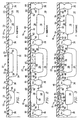
- a (p-) silicon substrate 10 is shown in a greatly enlarged and schematic view.
- Silicon substrate 10 may have either (100) or (111) crystallographic orientation, although (100) orientation is preferred.
- an (n+) buried region 16 is masked in oxide layer 12 to limits 17 in a (p) channel JFET area of the substrate indicated generally at 19.
- the sheet resistance of the buried collector region 14 and JFET buried region 16 should be approximately 15 Ohms/square, and a preferred dopant is antimony.
- substrate 10 is subjected to a thermal diffusion step to give the respective approximate conductivity type boundaries 18 and 20 of the buried regions 14 and 16 as shown.
- oxide portions such as portions 22, will grow back wherever the outer surface 23 of the silicon substrate 10 has been exposed before the previous implantation step.
- oxide layer 12 is removed within limits 25 and an (n-) buried region 24 is implanted and thermally diffused within a vertical PNP transistor area indicated generally at 27.
- the dopant concentration used to implant buried region 24 is much less than that of collector region 14 and JFET buried region 16, as using the same dopant level would overwhelm the vertical PNP collector region subsequently formed and described immediately below.
- -the oxide layer 12 is again removed within limits 26 to mask an implantation step for forming a (p) vertical PNP transistor collector region 28.
- a preferred implanted dopant species is boron.
- the (p) dopant is diffused by means of a thermal cycle such that the approximate final limit between (p) type and (n) type material is marked by boundary 30.
- the distance between boundary 30 of VPNP transistor collector region 28 and the boundary 32 of buried region 24 must be sufficient to isolate collector region 28 from the (p-) substrate 10, and to withstand more than the maximum operating voltage potential and not have a punch-through voltage breakdown.
- oxide is removed within limits 34 such that the (p) type dopant implanted into region 28 will also be implanted into a plurality of deep junction isolation regions 36. Regions 36 are provided to isolate the devices from each other such that parasitic transistor devices will not be formed.
- oxide layer 12 is stripped and an (n-) epitaxial silicon layer 38 is grown on the surface 23 of semiconductor substrate 10.
- a second oxide layer 40 is grown from an outer surface 42 of epitaxial layer 38.
- Oxide layer 40 is next removed within limits 44 to provide a mask for the next implantation step, which is a heavy deposition of (p) type dopant.
- the (p) dopant is diffused in a subsequent thermal cycle to create shallow (p+) junction isolation regions 46 and a (p+) deep collector region 48.
- Each shallow isolation region 46 overlies a respective deep isolation region 36, and region 48 overlies VPNP buried collector region 28.
- Deep collector region 48 is preferably annular or otherwise endless.
- the deposition of the (p) dopant is followed by a thermal diffusion drive-in step such that shallow junction isolation regions 46 become continuous with deep junction isolation regions 36, and such that deep collector region 48 will become continuous with buried collector region 28.
- dopant diffuses upwardly from semiconductor substrate 10 at the same time that dopant diffuses downwardly from the surface of epitaxial layer 38. This up-diffusion establishes upper boundaries 50 of collector regions 14 and 16 and upper boundary 52 of VPNP collector region 28.
- oxide layer 40 is removed within limits 57 and an (n) type dopant is implanted therein to form an (n-) base region 58 for the VPNP transistor. Subsequently, oxide layer 40 is removed within limits 60 to permit the implantation of an (n) type dopant such as antimony.
- a thermal diffusion drive-in step is conducted on epitaxial layer 38 such that the (n) type dopant implanted between limits 57 and between limits 60 diffuses to create threshold adjust regions 62 and to set VPNP base region 58.
- Threshold adjust regions 62 are desirable to prevent parasitic PMOS transistors between (p) diffusions, such as diffused regions 46 and 48. Threshold adjust regions 62 control the junction breakdown voltage such that it can exceed the standard 45-volt operating voltage.
- oxide layer 40 is removed within limits 64 in NPN transistor area 15, VPNP transistor area 27, and JFET area 19. Then, a (p) type dopant is deposited and thermally diffused to create a (p+) NPN transistor base region 66, a VPNP transistor (p+) emitter region 70, an annular or endless (p+) contact region 72 inside VPNP deep collector region 48, a (p+) JFET source region 74 and a (p+) JFET drain region 76.
- high sheet resistance resistors may be patterned by removal of certain portions of oxide layer 40 (not shown) with a subsequent oxidation and implantation to create the resistors (not shown) in layer 38.
- oxide is removed from oxide layer 40 down to the surface 42 of the epitaxial layer 38 within limits 78 in all three device areas 15, 19 and 27 for masking the deposition of an (n) type dopant.
- the dopant thus deposited is subsequently thermally diffused to create a conventional vertical NPN emitter region 80, a collector contact region 82 for the conventional NPN transistor, a vertical PNP base contact region 84, a'buried region contact 86 for ohmic contact to buried region 24, and a JFET gate contact region 88.
- base contact region 84 is annular or otherwise endless.
- FIGURE 3a a sectional detailed view is shown in FIGURE 3a.
- Field oxide 40 is removed between limits 90 and a thin gate oxide 92 is grown over the exposed surface of epitaxial layer 38.
- An (n) type dopant preferably phosphorus, is next implanted through gate oxide 92 to ,form a top gate region 94 that extends from gate contact region 88 to both source region 74 and drain region 76.
- a layer of photoresist (not shown) is used to mask all areas of gate oxide 92 except a window extending from drain region 76 to source region 74. This remaining exposed area is subjected to a boron implantation step to create a JFET channel region 96 that extends from source region 74 to drain region 76.
- FIGURE 4 The final steps of the preferred process are shown in FIGURE 4.
- the photoresist is stripped and a middle-level oxide layer 98 is deposited over the surface of oxide layer 40.
- Middle-level oxide layer 98 is then densified in a thermal step.
- a plurality of contact orifices 100 are next patterned and etched into middle-level oxide layer 98.
- the middle-level oxide layer 98 is then reflowed into the contact orifices 100 to produce sloping sidewalls thereof.
- a respective orifice 102 in field oxide layer 40 is opened below each contact orifice 100 to expose the surface 42 of the epitaxial layer 38 therebeneath.
- Metal leads 104-118 are then deposited, patterned and etched according to conventional methodology.
- middle level oxide portion 120 that is left over JFET channel 96.
- Top gate metal lead 117 is patterned and etched not only to contact gate contact region 88, but to extend over channel 96 spaced therefrom by middle level oxide portion 120.
- middle level oxide portion 120 allows the achievement of up to 45 volts in operating voltage.
- the standard (p) channel JFET without middle level oxide portion 120 would only operate up to a limit of approximately 32 to 33 volts because of problems associated with the electric field intensification at the drain/top gate junction.
- Middle level oxide portion 120 reduces the field intensification that occurs there, and allows the breakdown voltage to be extended out to as much as 50 volts. Middle level oxide portion 120 therefore allows the construction of a 45-volt chip.
- a passivating nitride layer (not shown) is preferably added thereafter to passivate the exposed surface of the completed integrated circuit.
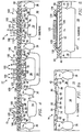
- FIGURE 5 is a greatly enlarged schematic cross sectional view of a capacitor that can be formed during the fabrication process of the other devices above described, with like numbers identifying like structure as appropriate.
- a deep isolation junction region 121 is implanted with a (p) type dopant at the same time that buried collector region 28 and deep junction isolation regions 36 (FIGURE 1) are implanted.
- the epitaxial layer 38 is then grown on semiconductor substrate 10 and second oxide layer 40 is grown on epitaxial layer 38.
- An orifice (not shown) is next opened into oxide layer 40 and a (p) type dopant is deposited on the surface 42 of layer 38 at the same time that the (p) type deposition is performed for shallow junction isolation regions 46 and deep collector region 48 (FIGURE 2).
- a thermal diffusion step is performed that up-diffuses dopant from region 121 and down-diffuses the dopant deposited on the surface 42 of epitaxial layer 38. This combined up-diffusion and .down-diffusion creates a continuous junction isolation region 122 that extends from epitaxial surface 42 into semiconductor substrate 10.
- a polycrystalline silicon layer is deposited, patterned with a photoresist mask, and etched to form a polysilicon electrode 124.
- Electrode 124 is rendered conductive by a heavy deposition of the (n) type dopant used to create emitter region 80, top gate contact region 88 and VPNP base contact region 84. The diffusion step by which the emitter dopant is diffused into regions 80, 84 and 88 will at the same time cause an oxide layer 126 to grow from the exposed surface of polysilicon electrode 124.
- Oxide layer 126 is removed within a central region 128 of the outer polysilicon surface. This central region 128 then has deposited on it a compressive-tension nitride dielectric layer 130 that is patterned and etched using conventional photoresist masking techniques to leave the portion of layer 130 shown.
- Middle level oxide layer 98 is deposited, densified, a contact opened therein, and reflowed at the same time that these steps are performed on the middle level oxide layer 98 as shown in FIGURE 4. Finally, an outer metal electrode 132 is deposited, patterned and etched at the same time that metal contacts 104-118 are formed.
Description
- This invention relates in general to the fabrication of different integrated circuit devices using a single semiconductor substrate, and more particularly to a process for simultaneously fabricating a junction field effect transistor (JFET) and a capacitor.
- Operational amplifier designs have always been limited in that conventional PNP integrated circuit transistors used therefor can operate only to around 5 megahertz. These PNP transistors in combination with conventional NPN transistors are typical devices found in operational amplifier integrated circuits.
- Recently, a high-frequency isolated vertical PNP (VPNP) transistor has been developed that is superior to the conventional and substrate PNP transistors. This isolated VPNP transistor is capable of 45-volt operation and exhibits a maximum operating frequency around 150 megahertz. The current gain and breakdown voltages on the isolated VPNP transistor are comparable to those achieved on the standard double diffused NPN transistor. Finally, the isolated VPNP is not limited to the emitter-follower configuration taken by the normal vertical substrate PNP transistor.
- Separately, a 50-volt (p) channel JFET has been developed to extend the gate-to-drain breakdown voltage past 45 volts. JFETs of this kind are conventionally used as operational amplifier inputs. These JFETs are achieved by using a thick deposited oxide over the gate oxide to reduce the electric field intensification at the top gate/drain reverse-biased p-n junction. This increases the gate-to-drain breakdown voltage from the low 30 volt range to approximately 50 volts. The gate-to-drain and gate-to-source oxides overlap capacitances are also reduced with the deposited oxide. This contributes to higher bandwidths and slew rates.
- Another desirable integrated circuit component is the metal/nitride/poly capacitor. The use of nitride in the place of oxide provides a doubling of the capacitance and allows for a dielectric breakdown in excess of 100 volts, and the fabrication of these capacitors on field oxide reduces parasitic junction capacitance and tank leakage currents.
- From Elektrotechnik und Maschinenbau, vol. 85, no. 10, 1968, pgs. 461-465, a monolithic integrated circuit including an NPN transistor, an (n) channel junction field effect transistor, a resistor and a capacitor formed within an (n) type layer on a (p) type substrate is known. The layers of the circuit are formed by diffusing dopants of different conductivity types into the silicon substrate. Heavily (p) doped junction isolation regions, which reach down into the substrate, are formed between the devices. An oxide layer having contact orifices is formed on the surface of the circuit.
- From EP-A-0 006 119 a process is known for the formation of an NPN transistor on a (p) type substrate merged with a JFET. The devices are formed in an epitaxial layer.
- From US-A-4 419 812 a method is known for the formation of a conductive polysilicon parallel plate capacitor and a polysilicon gate enhancement mode transistor for a voltage multiplier on a semiconductive substrate of a first conductivity type having an active region of a second conductivity type and a field isolation oxide region.
- In Microelectronics Journal, vol.13, no. 4, July 1982, pgs. 29 to 36, different capacitor structures that are integratable to a production NMOS or N well CMOS process are described. In one category of capacitor structure, the lower capacitor plate, which is made of polysilicon, is situated over a 1 µm thick field oxide. The upper plate is made of aluminum. The dielectric layer is an oxide layer or an oxide-nitride sandwich.
- It is therefore desirable to develop a process for the fabrication of an integrated circuit including a JFET and a capacitor of the kind described above. As yet, no such process has been heretofore developed, limiting circuit designers to the use of one of these circuit devices without the others in any one integrated circuit.
- One aspect of the present invention comprises a process for the simultaneous fabrication of a junction field effect transistor (JFET) and a capacitor using a single semiconductor substrate comprising the steps defined in claim 1.
- The incorporation of the fabrication steps of these devices into a single process flow has the advantage of greatly reducing the number of mask levels required for the separate fabrication of each. An integrated circuit containing these devices gives integrated circuit designers much more leeway and flexibility than the more conventional devices that they supplement. The process is compatible with more conventional 45 volt vertical NPN transistors, high sheet resistors, 45 volt threshold voltages, and other common features of JFET fabrication processes. The double (up and down) diffused isolation preferably used in the construction of the devices of the invention allows for a tighter design layout and can save up to 25% layout area on spacing relative to single-diffusion isolation.
- Other aspects of the invention and their advantages will become apparent by referring to the following detailed description in conjunction with the drawings in which:
- FIGURES 1-4 are greatly enlarged schematic sections showing successive stages of fabricating a vertical PNP transistor, a p-channel JFET and a vertical NPN transistor useful for understanding the present invention;
- FIGURE 3a is a detail of the sectional view shown in FIGURE 3, showing additional JFET fabrication steps; and
- FIGURE 5 is a greatly enlarged schematic sectional view of a metal/nitride/polysilicon capacitor that is fabricated in conjunction with the devices shown in FIGURES 1-4.
-
- Referring first to FIGURE 1, a (p-)
silicon substrate 10 is shown in a greatly enlarged and schematic view.Silicon substrate 10 may have either (100) or (111) crystallographic orientation, although (100) orientation is preferred. Aninitial oxide layer 12, here shown after several patternings, etches and regrowths of replacement oxide, is grown onsubstrate 10. After this, a portion ofoxide layer 12 between limits 13 (schematically shown by hash marks) is removed using conventional pattern-and-etch techniques to create a mask for the implantation of an (n+) buriedcollector region 14 for an NPN vertical transistor in an NPN bipolar transistor area indicated generally at 15. At the same time, an (n+) buriedregion 16 is masked inoxide layer 12 to limits 17 in a (p) channel JFET area of the substrate indicated generally at 19. The sheet resistance of the buriedcollector region 14 and JFET buriedregion 16 should be approximately 15 Ohms/square, and a preferred dopant is antimony. - After the implantation of the dopant,
substrate 10 is subjected to a thermal diffusion step to give the respective approximateconductivity type boundaries 18 and 20 of the buriedregions portions 22, will grow back wherever theouter surface 23 of thesilicon substrate 10 has been exposed before the previous implantation step. - Next,
oxide layer 12 is removed withinlimits 25 and an (n-) buriedregion 24 is implanted and thermally diffused within a vertical PNP transistor area indicated generally at 27. The dopant concentration used to implant buriedregion 24 is much less than that ofcollector region 14 and JFET buriedregion 16, as using the same dopant level would overwhelm the vertical PNP collector region subsequently formed and described immediately below. - In a similar manner, -the
oxide layer 12 is again removed withinlimits 26 to mask an implantation step for forming a (p) vertical PNPtransistor collector region 28. A preferred implanted dopant species is boron. The (p) dopant is diffused by means of a thermal cycle such that the approximate final limit between (p) type and (n) type material is marked byboundary 30. The distance betweenboundary 30 of VPNPtransistor collector region 28 and theboundary 32 of buriedregion 24 must be sufficient to isolatecollector region 28 from the (p-)substrate 10, and to withstand more than the maximum operating voltage potential and not have a punch-through voltage breakdown. - Simultaneously with the removal of oxide from
layer 12 withinlimits 26, oxide is removed withinlimits 34 such that the (p) type dopant implanted intoregion 28 will also be implanted into a plurality of deepjunction isolation regions 36.Regions 36 are provided to isolate the devices from each other such that parasitic transistor devices will not be formed. - Turning now to FIGURE 2,
oxide layer 12 is stripped and an (n-)epitaxial silicon layer 38 is grown on thesurface 23 ofsemiconductor substrate 10. Asecond oxide layer 40 is grown from anouter surface 42 ofepitaxial layer 38. -
Oxide layer 40 is next removed withinlimits 44 to provide a mask for the next implantation step, which is a heavy deposition of (p) type dopant. The (p) dopant is diffused in a subsequent thermal cycle to create shallow (p+)junction isolation regions 46 and a (p+)deep collector region 48. Eachshallow isolation region 46 overlies a respectivedeep isolation region 36, andregion 48 overlies VPNP buriedcollector region 28.Deep collector region 48 is preferably annular or otherwise endless. - The deposition of the (p) dopant is followed by a thermal diffusion drive-in step such that shallow
junction isolation regions 46 become continuous with deepjunction isolation regions 36, and such thatdeep collector region 48 will become continuous with buriedcollector region 28. In this diffusion step, dopant diffuses upwardly fromsemiconductor substrate 10 at the same time that dopant diffuses downwardly from the surface ofepitaxial layer 38. This up-diffusion establishesupper boundaries 50 ofcollector regions VPNP collector region 28. - In the various diffusion steps conducted, it is important to balance the thermal cycles in order to get the proper amount of diffusion. Hence, earlier-created structures should be subjected to a less severe thermal cycle than later-created structures if all other parameters are the same, because the later thermal cycles will affect the extent and concentrations of earlier created structures as well as the later ones.
- Next,
oxide layer 40 is removed withinlimits 57 and an (n) type dopant is implanted therein to form an (n-)base region 58 for the VPNP transistor. Subsequently,oxide layer 40 is removed withinlimits 60 to permit the implantation of an (n) type dopant such as antimony. After this implantation, a thermal diffusion drive-in step is conducted onepitaxial layer 38 such that the (n) type dopant implanted betweenlimits 57 and betweenlimits 60 diffuses to create threshold adjustregions 62 and to setVPNP base region 58. Threshold adjustregions 62 are desirable to prevent parasitic PMOS transistors between (p) diffusions, such as diffusedregions regions 62 control the junction breakdown voltage such that it can exceed the standard 45-volt operating voltage. - Turning now to FIGURE 3, a portion of
oxide layer 40 is removed withinlimits 64 inNPN transistor area 15,VPNP transistor area 27, andJFET area 19. Then, a (p) type dopant is deposited and thermally diffused to create a (p+) NPNtransistor base region 66, a VPNP transistor (p+)emitter region 70, an annular or endless (p+)contact region 72 inside VPNPdeep collector region 48, a (p+)JFET source region 74 and a (p+)JFET drain region 76. After this step, high sheet resistance resistors (not shown) may be patterned by removal of certain portions of oxide layer 40 (not shown) with a subsequent oxidation and implantation to create the resistors (not shown) inlayer 38. - Next, oxide is removed from
oxide layer 40 down to thesurface 42 of theepitaxial layer 38 withinlimits 78 in all threedevice areas NPN emitter region 80, acollector contact region 82 for the conventional NPN transistor, a vertical PNPbase contact region 84,a'buried region contact 86 for ohmic contact to buriedregion 24, and a JFETgate contact region 88. In the embodiment shown,base contact region 84 is annular or otherwise endless. - To illustrate further steps in the fabrication of the JFET, a sectional detailed view is shown in FIGURE 3a.
Field oxide 40 is removed betweenlimits 90 and athin gate oxide 92 is grown over the exposed surface ofepitaxial layer 38. An (n) type dopant, preferably phosphorus, is next implanted throughgate oxide 92 to ,form atop gate region 94 that extends fromgate contact region 88 to bothsource region 74 and drainregion 76. After this implantation step, a layer of photoresist (not shown) is used to mask all areas ofgate oxide 92 except a window extending fromdrain region 76 to sourceregion 74. This remaining exposed area is subjected to a boron implantation step to create aJFET channel region 96 that extends fromsource region 74 to drainregion 76. - The final steps of the preferred process are shown in FIGURE 4. The photoresist is stripped and a middle-
level oxide layer 98 is deposited over the surface ofoxide layer 40. Middle-level oxide layer 98 is then densified in a thermal step. A plurality ofcontact orifices 100 are next patterned and etched into middle-level oxide layer 98. The middle-level oxide layer 98 is then reflowed into thecontact orifices 100 to produce sloping sidewalls thereof. Arespective orifice 102 infield oxide layer 40 is opened below eachcontact orifice 100 to expose thesurface 42 of theepitaxial layer 38 therebeneath. Metal leads 104-118 are then deposited, patterned and etched according to conventional methodology. - An important aspect of the invention is the existence of a middle
level oxide portion 120 that is left overJFET channel 96. Topgate metal lead 117 is patterned and etched not only to contactgate contact region 88, but to extend overchannel 96 spaced therefrom by middlelevel oxide portion 120. The existence of middlelevel oxide portion 120 allows the achievement of up to 45 volts in operating voltage. The standard (p) channel JFET without middlelevel oxide portion 120 would only operate up to a limit of approximately 32 to 33 volts because of problems associated with the electric field intensification at the drain/top gate junction. Middlelevel oxide portion 120 reduces the field intensification that occurs there, and allows the breakdown voltage to be extended out to as much as 50 volts. Middlelevel oxide portion 120 therefore allows the construction of a 45-volt chip. A passivating nitride layer (not shown) is preferably added thereafter to passivate the exposed surface of the completed integrated circuit. - FIGURE 5 is a greatly enlarged schematic cross sectional view of a capacitor that can be formed during the fabrication process of the other devices above described, with like numbers identifying like structure as appropriate. In a separate area of (p)
type semiconductor substrate 10, a deepisolation junction region 121 is implanted with a (p) type dopant at the same time that buriedcollector region 28 and deep junction isolation regions 36 (FIGURE 1) are implanted. Theepitaxial layer 38 is then grown onsemiconductor substrate 10 andsecond oxide layer 40 is grown onepitaxial layer 38. An orifice (not shown) is next opened intooxide layer 40 and a (p) type dopant is deposited on thesurface 42 oflayer 38 at the same time that the (p) type deposition is performed for shallowjunction isolation regions 46 and deep collector region 48 (FIGURE 2). Next, a thermal diffusion step is performed that up-diffuses dopant fromregion 121 and down-diffuses the dopant deposited on thesurface 42 ofepitaxial layer 38. This combined up-diffusion and .down-diffusion creates a continuousjunction isolation region 122 that extends fromepitaxial surface 42 intosemiconductor substrate 10. - Prior to the doping/diffusion sequence that creates
NPN emitter region 80, VPNPbase contact region 84 and JFET gate contact region 88 (FIGURE 3), a polycrystalline silicon layer is deposited, patterned with a photoresist mask, and etched to form apolysilicon electrode 124.Electrode 124 is rendered conductive by a heavy deposition of the (n) type dopant used to createemitter region 80, topgate contact region 88 and VPNPbase contact region 84. The diffusion step by which the emitter dopant is diffused intoregions oxide layer 126 to grow from the exposed surface ofpolysilicon electrode 124. -
Oxide layer 126 is removed within acentral region 128 of the outer polysilicon surface. Thiscentral region 128 then has deposited on it a compressive-tensionnitride dielectric layer 130 that is patterned and etched using conventional photoresist masking techniques to leave the portion oflayer 130 shown. - Middle
level oxide layer 98 is deposited, densified, a contact opened therein, and reflowed at the same time that these steps are performed on the middlelevel oxide layer 98 as shown in FIGURE 4. Finally, anouter metal electrode 132 is deposited, patterned and etched at the same time that metal contacts 104-118 are formed. - In summary, a unified process for the fabrication of a vertical PNP transistor, a (p) channel JFET transistor and a metal/nitride/polysilicon capacitor, as well as conventional vertical NPN transistors and other standard devices used in linear bipolar/JFET integrated circuits, has been shown and described. The unified process eliminates many masking steps and permits increased flexibility in circuit design.
Claims (2)
- A process for fabricating a junction field effect transistor (JFET) and a capacitor using a single semiconductor substrate of a first conductivity type, comprising the steps of:forming a buried region (16) of a first conductivity type at a face of the semiconductor substrate (10);simultaneously forming at least two deep junction isolation regions at the face to be of the first conductivity type, the first deep junction isolation region (36) formed between a JFET area (19) of the substrate (10) and a capacitor area of the substrate (10), the second junction isolation region (121) formed within the capacitor area;forming an epitaxial layer (38) of the second conductivity type on the face;forming an insulator layer (40) on an outer face of the epitaxial layer (38);up-diffusing dopant to extend the buried region (16) and the deep junction isolation regions (36, 121) into the epitaxial layer (38);simultaneously forming at least two shallow junction isolation regions of the first conductivity type at the outer face of the epitaxial layer (38), each shallow junction isolation region formed to be continuous with a respective deep junction isolation region (36, 121);forming a polycrystalline layer including silicon on the insulator layer (40) over the second shallow junction isolation region;forming a middle-level insulating layer over the polycrystalline layer and the insulating layer (40);opening orifices in the middle-level insulating layer to the polycrystalline layer and to a region of the insulating layer over a gate contact region (88) of the epitaxial layer (38) in the JFET area (19);removing the region of the insulating layer to expose the gate contact region (88); andsimultaneously doping the polycrystalline layer and the gate contact region to respectively form a conductive capacitor electrode (124) and a top gate contact.
- The process of claim 1, wnerein said insulator layer (40) comprises silicon dioxide, the process comprising the further step of thermally growing at least a portion of the insulator layer (40) during said step of up-diffusing dopant.
Applications Claiming Priority (3)
| Application Number | Priority Date | Filing Date | Title |
|---|---|---|---|
| US21164188A | 1988-06-27 | 1988-06-27 | |
| US211641 | 1988-06-27 | ||
| EP89107212A EP0348626B1 (en) | 1988-06-27 | 1989-04-21 | Process for fabricating isolated vertical bipolar and JFET transistors and corresponding IC |
Related Parent Applications (2)
| Application Number | Title | Priority Date | Filing Date |
|---|---|---|---|
| EP89107212.6 Division | 1989-04-21 | ||
| EP89107212A Division EP0348626B1 (en) | 1988-06-27 | 1989-04-21 | Process for fabricating isolated vertical bipolar and JFET transistors and corresponding IC |
Publications (2)
| Publication Number | Publication Date |
|---|---|
| EP0627767A1 EP0627767A1 (en) | 1994-12-07 |
| EP0627767B1 true EP0627767B1 (en) | 2002-11-06 |
Family
ID=22787775
Family Applications (2)
| Application Number | Title | Priority Date | Filing Date |
|---|---|---|---|
| EP89107212A Expired - Lifetime EP0348626B1 (en) | 1988-06-27 | 1989-04-21 | Process for fabricating isolated vertical bipolar and JFET transistors and corresponding IC |
| EP94112898A Expired - Lifetime EP0627767B1 (en) | 1988-06-27 | 1989-04-21 | Process for fabricating JFET transistors and capacitors |
Family Applications Before (1)
| Application Number | Title | Priority Date | Filing Date |
|---|---|---|---|
| EP89107212A Expired - Lifetime EP0348626B1 (en) | 1988-06-27 | 1989-04-21 | Process for fabricating isolated vertical bipolar and JFET transistors and corresponding IC |
Country Status (4)
| Country | Link |
|---|---|
| EP (2) | EP0348626B1 (en) |
| JP (2) | JPH0691192B2 (en) |
| KR (1) | KR0169097B1 (en) |
| DE (2) | DE68928763T2 (en) |
Families Citing this family (6)
| Publication number | Priority date | Publication date | Assignee | Title |
|---|---|---|---|---|
| GB2305776B (en) * | 1995-09-28 | 1999-11-17 | Gresham Sensor Technology Limi | Charge amplifier |
| EP0849771A1 (en) * | 1996-12-19 | 1998-06-24 | Motorola Semiconducteurs S.A. | Method of forming a depletion jfet and method of forming a depletion jfet and a bipolar transistor on a semiconductor substrate |
| JP3530414B2 (en) | 1999-03-26 | 2004-05-24 | 三洋電機株式会社 | Semiconductor device |
| WO2011109442A2 (en) | 2010-03-02 | 2011-09-09 | Oliver Steven D | Led packaging with integrated optics and methods of manufacturing the same |
| US11482521B2 (en) * | 2020-02-06 | 2022-10-25 | Globalfoundries U.S. Inc. | Integrated circuit with P-N-P junction and vertically aligned field effect transistor, and method to form same |
| CN113097309A (en) * | 2021-03-31 | 2021-07-09 | 上海晶丰明源半导体股份有限公司 | Junction field effect transistor and semiconductor device |
Family Cites Families (6)
| Publication number | Priority date | Publication date | Assignee | Title |
|---|---|---|---|---|
| FR1559609A (en) * | 1967-06-30 | 1969-03-14 | ||
| JPS553691A (en) * | 1978-06-13 | 1980-01-11 | Ibm | Integrated circuit having junction field effect transistor |
| US4322738A (en) * | 1980-01-21 | 1982-03-30 | Texas Instruments Incorporated | N-Channel JFET device compatible with existing bipolar integrated circuit processing techniques |
| JPS57128073A (en) * | 1981-12-21 | 1982-08-09 | Hitachi Ltd | Semiconductor integrated circuit device |
| US4419812A (en) * | 1982-08-23 | 1983-12-13 | Ncr Corporation | Method of fabricating an integrated circuit voltage multiplier containing a parallel plate capacitor |
| JPS60117765A (en) * | 1983-11-30 | 1985-06-25 | Fujitsu Ltd | Manufacture of semiconductor device |
-
1989
- 1989-04-21 DE DE68928763T patent/DE68928763T2/en not_active Expired - Fee Related
- 1989-04-21 EP EP89107212A patent/EP0348626B1/en not_active Expired - Lifetime
- 1989-04-21 EP EP94112898A patent/EP0627767B1/en not_active Expired - Lifetime
- 1989-04-21 DE DE68929433T patent/DE68929433T2/en not_active Expired - Fee Related
- 1989-06-22 KR KR1019890008629A patent/KR0169097B1/en not_active IP Right Cessation
- 1989-06-26 JP JP1161014A patent/JPH0691192B2/en not_active Expired - Fee Related
-
1991
- 1991-04-26 JP JP3095933A patent/JPH04226061A/en active Pending
Also Published As
| Publication number | Publication date |
|---|---|
| JPH0251264A (en) | 1990-02-21 |
| DE68929433D1 (en) | 2002-12-12 |
| KR0169097B1 (en) | 1999-01-15 |
| EP0627767A1 (en) | 1994-12-07 |
| KR900001036A (en) | 1990-01-31 |
| EP0348626A3 (en) | 1991-07-31 |
| EP0348626A2 (en) | 1990-01-03 |
| DE68928763D1 (en) | 1998-09-10 |
| DE68929433T2 (en) | 2003-06-26 |
| EP0348626B1 (en) | 1998-08-05 |
| DE68928763T2 (en) | 1999-04-08 |
| JPH04226061A (en) | 1992-08-14 |
| JPH0691192B2 (en) | 1994-11-14 |
Similar Documents
| Publication | Publication Date | Title |
|---|---|---|
| US4939099A (en) | Process for fabricating isolated vertical bipolar and JFET transistors | |
| US4694562A (en) | Method for manufacturing a semiconductor integrated device including bipolar and CMOS transistors | |
| US4445268A (en) | Method of manufacturing a semiconductor integrated circuit BI-MOS device | |
| US5171699A (en) | Vertical DMOS transistor structure built in an N-well CMOS-based BiCMOS process and method of fabrication | |
| US4628341A (en) | Integrated circuit structure comprising CMOS transistors having high blocking voltage capability and method of fabrication of said structure | |
| US5382538A (en) | Method for forming MOS transistors having vertical current flow and resulting structure | |
| US6365447B1 (en) | High-voltage complementary bipolar and BiCMOS technology using double expitaxial growth | |
| US5034338A (en) | Circuit containing integrated bipolar and complementary MOS transistors on a common substrate | |
| US4510676A (en) | Method of fabricating a lateral PNP transistor | |
| US5557131A (en) | Elevated emitter for double poly BICMOS devices | |
| US6033947A (en) | Driving circuit for electronic semiconductor devices including at least a power transistor | |
| KR910006672B1 (en) | Semiconductor integrated circuit device and its manufacturing method | |
| US4994887A (en) | High voltage merged bipolar/CMOS technology | |
| KR0134887B1 (en) | Dipole transistor manufacturing method | |
| JPH10214907A (en) | Semiconductor device and its manufacture | |
| EP0423791B1 (en) | MIS capacitive element | |
| EP0627767B1 (en) | Process for fabricating JFET transistors and capacitors | |
| EP0481454B1 (en) | Lateral MOSFET and manufacturing method thereof | |
| US5300451A (en) | Process for forming a buried drain or collector region in monolithic semiconductor devices | |
| EP0267882A1 (en) | Monolithic integration of isolated, high performance, power vdmos transistors and of high voltage p-channel mos transistors together with cmos, npn, pnp transistors and low leakage diodes | |
| US6501152B1 (en) | Advanced lateral PNP by implant negation | |
| EP0347550A2 (en) | Process for fabricating isolated vertical and super beta bipolar transistors | |
| EP0792514B1 (en) | Method of making an integrated circuit with complementary isolated bipolar transitors | |
| US4197147A (en) | Method of manufacturing an integrated circuit including an analog circuit and an I2 L circuit utilizing staged diffusion techniques | |
| US20090026578A1 (en) | Vertical NPN Transistor Fabricated in a CMOS Process With Improved Electrical Characteristics |
Legal Events
| Date | Code | Title | Description |
|---|---|---|---|
| PUAI | Public reference made under article 153(3) epc to a published international application that has entered the european phase |
Free format text: ORIGINAL CODE: 0009012 |
|
| AC | Divisional application: reference to earlier application |
Ref document number: 348626 Country of ref document: EP |
|
| AK | Designated contracting states |
Kind code of ref document: A1 Designated state(s): DE FR GB IT NL |
|
| 17P | Request for examination filed |
Effective date: 19950512 |
|
| 17Q | First examination report despatched |
Effective date: 19970618 |
|
| RTI1 | Title (correction) |
Free format text: PROCESS FOR FABRICATING JFET TRANSISTORS AND CAPACITORS |
|
| GRAG | Despatch of communication of intention to grant |
Free format text: ORIGINAL CODE: EPIDOS AGRA |
|
| GRAG | Despatch of communication of intention to grant |
Free format text: ORIGINAL CODE: EPIDOS AGRA |
|
| GRAH | Despatch of communication of intention to grant a patent |
Free format text: ORIGINAL CODE: EPIDOS IGRA |
|
| GRAH | Despatch of communication of intention to grant a patent |
Free format text: ORIGINAL CODE: EPIDOS IGRA |
|
| GRAA | (expected) grant |
Free format text: ORIGINAL CODE: 0009210 |
|
| AC | Divisional application: reference to earlier application |
Ref document number: 348626 Country of ref document: EP |
|
| AK | Designated contracting states |
Kind code of ref document: B1 Designated state(s): DE FR GB IT NL |
|
| PG25 | Lapsed in a contracting state [announced via postgrant information from national office to epo] |
Ref country code: NL Free format text: LAPSE BECAUSE OF FAILURE TO SUBMIT A TRANSLATION OF THE DESCRIPTION OR TO PAY THE FEE WITHIN THE PRESCRIBED TIME-LIMIT Effective date: 20021106 Ref country code: IT Free format text: LAPSE BECAUSE OF FAILURE TO SUBMIT A TRANSLATION OF THE DESCRIPTION OR TO PAY THE FEE WITHIN THE PRE;WARNING: LAPSES OF ITALIAN PATENTS WITH EFFECTIVE DATE BEFORE 2007 MAY HAVE OCCURRED AT ANY TIME BEFORE 2007. THE CORRECT EFFECTIVE DATE MAY BE DIFFERENT FROM THE ONE RECORDED.SCRIBED TIME-LIMIT Effective date: 20021106 |
|
| REG | Reference to a national code |
Ref country code: GB Ref legal event code: FG4D |
|
| REF | Corresponds to: |
Ref document number: 68929433 Country of ref document: DE Date of ref document: 20021212 |
|
| NLV1 | Nl: lapsed or annulled due to failure to fulfill the requirements of art. 29p and 29m of the patents act | ||
| ET | Fr: translation filed | ||
| PLBE | No opposition filed within time limit |
Free format text: ORIGINAL CODE: 0009261 |
|
| STAA | Information on the status of an ep patent application or granted ep patent |
Free format text: STATUS: NO OPPOSITION FILED WITHIN TIME LIMIT |
|
| 26N | No opposition filed |
Effective date: 20030807 |
|
| PGFP | Annual fee paid to national office [announced via postgrant information from national office to epo] |
Ref country code: GB Payment date: 20070313 Year of fee payment: 19 |
|
| PGFP | Annual fee paid to national office [announced via postgrant information from national office to epo] |
Ref country code: DE Payment date: 20070430 Year of fee payment: 19 |
|
| PGFP | Annual fee paid to national office [announced via postgrant information from national office to epo] |
Ref country code: FR Payment date: 20070404 Year of fee payment: 19 |
|
| GBPC | Gb: european patent ceased through non-payment of renewal fee |
Effective date: 20080421 |
|
| PG25 | Lapsed in a contracting state [announced via postgrant information from national office to epo] |
Ref country code: DE Free format text: LAPSE BECAUSE OF NON-PAYMENT OF DUE FEES Effective date: 20081101 |
|
| REG | Reference to a national code |
Ref country code: FR Ref legal event code: ST Effective date: 20081231 |
|
| PG25 | Lapsed in a contracting state [announced via postgrant information from national office to epo] |
Ref country code: FR Free format text: LAPSE BECAUSE OF NON-PAYMENT OF DUE FEES Effective date: 20080430 |
|
| PG25 | Lapsed in a contracting state [announced via postgrant information from national office to epo] |
Ref country code: GB Free format text: LAPSE BECAUSE OF NON-PAYMENT OF DUE FEES Effective date: 20080421 |