EP0620557A2 - Anordnung zur Speicherdefekterkennung - Google Patents
Anordnung zur Speicherdefekterkennung Download PDFInfo
- Publication number
- EP0620557A2 EP0620557A2 EP94301875A EP94301875A EP0620557A2 EP 0620557 A2 EP0620557 A2 EP 0620557A2 EP 94301875 A EP94301875 A EP 94301875A EP 94301875 A EP94301875 A EP 94301875A EP 0620557 A2 EP0620557 A2 EP 0620557A2
- Authority
- EP
- European Patent Office
- Prior art keywords
- column
- cells
- memory cells
- defect
- bit lines
- Prior art date
- Legal status (The legal status is an assumption and is not a legal conclusion. Google has not performed a legal analysis and makes no representation as to the accuracy of the status listed.)
- Withdrawn
Links
Images
Classifications
-
- G—PHYSICS
- G11—INFORMATION STORAGE
- G11C—STATIC STORES
- G11C29/00—Checking stores for correct operation ; Subsequent repair; Testing stores during standby or offline operation
- G11C29/04—Detection or location of defective memory elements, e.g. cell constructio details, timing of test signals
- G11C29/08—Functional testing, e.g. testing during refresh, power-on self testing [POST] or distributed testing
- G11C29/12—Built-in arrangements for testing, e.g. built-in self testing [BIST] or interconnection details
- G11C29/44—Indication or identification of errors, e.g. for repair
-
- G—PHYSICS
- G11—INFORMATION STORAGE
- G11C—STATIC STORES
- G11C29/00—Checking stores for correct operation ; Subsequent repair; Testing stores during standby or offline operation
- G11C29/04—Detection or location of defective memory elements, e.g. cell constructio details, timing of test signals
- G11C29/50—Marginal testing, e.g. race, voltage or current testing
-
- G—PHYSICS
- G11—INFORMATION STORAGE
- G11C—STATIC STORES
- G11C11/00—Digital stores characterised by the use of particular electric or magnetic storage elements; Storage elements therefor
- G11C11/21—Digital stores characterised by the use of particular electric or magnetic storage elements; Storage elements therefor using electric elements
- G11C11/34—Digital stores characterised by the use of particular electric or magnetic storage elements; Storage elements therefor using electric elements using semiconductor devices
- G11C11/40—Digital stores characterised by the use of particular electric or magnetic storage elements; Storage elements therefor using electric elements using semiconductor devices using transistors
- G11C11/41—Digital stores characterised by the use of particular electric or magnetic storage elements; Storage elements therefor using electric elements using semiconductor devices using transistors forming static cells with positive feedback, i.e. cells not needing refreshing or charge regeneration, e.g. bistable multivibrator or Schmitt trigger
Definitions
- the present invention is concerned with an arrangement for detecting defects in static random access memories, and in particular although not exclusively with an arrangement for detecting open circuit or "soft" defects in six-transistor memory cells.
- a number of spare circuits or memory cells may be provided on the chip so that during testing any failed circuit or block of memory cells may be replaced by a spare, for example by blowing fuse links, in order to minimise the number of chips rejected.
- an open circuit or soft defect detection arrangement comprises, in respect of a column of memory cells of the array, means to lower the supply voltage to the cells of said column of memory cells, means to apply a sequence of test signal levels to the bit lines of said column of memory cells, and means to indicate an open circuit defect in one or more of the cells of said column from the response to said test signal levels.
- said means to indicate an open circuit defect in one or more cells of said column comprises a latch circuit the outputs of which are connectable to said bit lines of said column whereby said column exhibiting said defect may be identified.
- the supply voltage to said column of cells may be switched to a predetermined reduced value for the period of the application of said test signal levels to said bit lines.
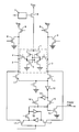
- the arrangement tests each of the six-transistor memory cells 1 of a column of cells in an array as two separate inverters, by testing each independently with high (V DD ) and low (earth) inputs, the presence of a defect being detected either by a cell not switching or switching more slowly than a good cell.
- This parasitic inverter can prevent a high on the respective bit line 2 or 3 from reaching the switching point of the inverter under test through the n-channel access transistor 4 due to the clamping effect of the n-channel driver transistor 5 of the parasitic inverter.
- This clamping effect can be overcome by reducing the conductance of this driver transistor 5 compared to that of the access transistor 4, by reducing the supply voltage to the memory cells 1 of the array during testing.
- the supply voltage to the memory cells 1 is reduced from V DD to a predetermined fraction of V DD by a series n-channel device 6 under the control of a circuit 7.
- the inverters within a memory cell 1 are connected to the bit lines 2 and 3 by respective access transistors such as 4, and during a test it is necessary to switch these access transistors on. In order to detect correct switching it is necessary to precharge the output bit line (2 or 3) to the opposite state to that expected. It is also necessary to apply both high (V DD ) and low (earth) signal levels to the input bit line (3 or 2), this being accomplished by one p-channel transistor 8 and one n-channel transistor 9 per bit line.
- bit lines 2 and 3 are selectively connected to the input of an inverting amplifier 10 by way of n-channel devices 11, the output of this amplifier in turn being connected to the input of a second inverting amplifier 12.
- An output from one or other of these amplifiers 10 and 12 is then applied, after an adequate time to allow the memory cell 1 to switch correctly, to an open source n-channel output transistor 13 and to a latch circuit 14 by way of respective n-channel transistors 15 and 16, depending on whether a low to high or a high to low test is taking place.
- the value stored in the latch circuit 15 may be applied to the bit lines 2 and 3 for sensing with a normal sensing amplifier by switching into conduction the n-channel devices 17, to identify the column location of a faulty cell 1.
- the tests are performed on alternate columns i.e. as one column is testing for a high to low transition of an inverter within a cell, the next is testing for a low to high.
- the arrangement can be disabled in order to reduce the current consumption of the circuit when not in use, by switching all precharging devices 8 and 9 off as well as the bit line selection transistors 11.
- a disable transistor is also introduced to apply a valid (low) input for the sense amplifier (not shown) when not in use.
- a soft defect test arrangement is required for every column within the array since any multiplexing of bit lines will invalidate the test. This means that arrays must be tested one row at a time. For a typical array of 64 rows and operating with V DD of 5 Volts the switching time of a cell is approximately 250ns. Four tests are required per row, thus the total time to test the array becomes 64us. This switching time is however increased for lower values of V DD to approximately 4us, producing a total test time of approximately 1ms.
Landscapes
- For Increasing The Reliability Of Semiconductor Memories (AREA)
- Techniques For Improving Reliability Of Storages (AREA)
- Static Random-Access Memory (AREA)
Applications Claiming Priority (2)
| Application Number | Priority Date | Filing Date | Title |
|---|---|---|---|
| GB9307648A GB2277161B (en) | 1993-04-14 | 1993-04-14 | Memory defect detection arrangement |
| GB9307648 | 1993-04-14 |
Publications (2)
| Publication Number | Publication Date |
|---|---|
| EP0620557A2 true EP0620557A2 (de) | 1994-10-19 |
| EP0620557A3 EP0620557A3 (de) | 1996-08-07 |
Family
ID=10733768
Family Applications (1)
| Application Number | Title | Priority Date | Filing Date |
|---|---|---|---|
| EP94301875A Withdrawn EP0620557A3 (de) | 1993-04-14 | 1994-03-16 | Anordnung zur Speicherdefekterkennung. |
Country Status (3)
| Country | Link |
|---|---|
| US (1) | US5500823A (de) |
| EP (1) | EP0620557A3 (de) |
| GB (1) | GB2277161B (de) |
Families Citing this family (27)
| Publication number | Priority date | Publication date | Assignee | Title |
|---|---|---|---|---|
| KR0157339B1 (ko) * | 1995-06-28 | 1998-12-01 | 김광호 | 반도체 메모리의 불량셀 구제회로 |
| US5870407A (en) * | 1996-05-24 | 1999-02-09 | Advanced Micro Devices, Inc. | Method of screening memory cells at room temperature that would be rejected during hot temperature programming tests |
| US5930185A (en) * | 1997-09-26 | 1999-07-27 | Advanced Micro Devices, Inc. | Data retention test for static memory cell |
| US8103496B1 (en) | 2000-10-26 | 2012-01-24 | Cypress Semicondutor Corporation | Breakpoint control in an in-circuit emulation system |
| US8149048B1 (en) | 2000-10-26 | 2012-04-03 | Cypress Semiconductor Corporation | Apparatus and method for programmable power management in a programmable analog circuit block |
| US8176296B2 (en) | 2000-10-26 | 2012-05-08 | Cypress Semiconductor Corporation | Programmable microcontroller architecture |
| US6724220B1 (en) | 2000-10-26 | 2004-04-20 | Cyress Semiconductor Corporation | Programmable microcontroller architecture (mixed analog/digital) |
| US8160864B1 (en) | 2000-10-26 | 2012-04-17 | Cypress Semiconductor Corporation | In-circuit emulator and pod synchronized boot |
| US7406674B1 (en) | 2001-10-24 | 2008-07-29 | Cypress Semiconductor Corporation | Method and apparatus for generating microcontroller configuration information |
| US8078970B1 (en) | 2001-11-09 | 2011-12-13 | Cypress Semiconductor Corporation | Graphical user interface with user-selectable list-box |
| US8042093B1 (en) | 2001-11-15 | 2011-10-18 | Cypress Semiconductor Corporation | System providing automatic source code generation for personalization and parameterization of user modules |
| US6971004B1 (en) | 2001-11-19 | 2005-11-29 | Cypress Semiconductor Corp. | System and method of dynamically reconfiguring a programmable integrated circuit |
| US7844437B1 (en) * | 2001-11-19 | 2010-11-30 | Cypress Semiconductor Corporation | System and method for performing next placements and pruning of disallowed placements for programming an integrated circuit |
| US8069405B1 (en) | 2001-11-19 | 2011-11-29 | Cypress Semiconductor Corporation | User interface for efficiently browsing an electronic document using data-driven tabs |
| US8103497B1 (en) | 2002-03-28 | 2012-01-24 | Cypress Semiconductor Corporation | External interface for event architecture |
| US7295049B1 (en) | 2004-03-25 | 2007-11-13 | Cypress Semiconductor Corporation | Method and circuit for rapid alignment of signals |
| US7332976B1 (en) * | 2005-02-04 | 2008-02-19 | Cypress Semiconductor Corporation | Poly-phase frequency synthesis oscillator |
| US7400183B1 (en) | 2005-05-05 | 2008-07-15 | Cypress Semiconductor Corporation | Voltage controlled oscillator delay cell and method |
| US8067948B2 (en) * | 2006-03-27 | 2011-11-29 | Cypress Semiconductor Corporation | Input/output multiplexer bus |
| US8040266B2 (en) * | 2007-04-17 | 2011-10-18 | Cypress Semiconductor Corporation | Programmable sigma-delta analog-to-digital converter |
| US8111577B2 (en) * | 2007-04-17 | 2012-02-07 | Cypress Semiconductor Corporation | System comprising a state-monitoring memory element |
| US8026739B2 (en) | 2007-04-17 | 2011-09-27 | Cypress Semiconductor Corporation | System level interconnect with programmable switching |
| US8130025B2 (en) | 2007-04-17 | 2012-03-06 | Cypress Semiconductor Corporation | Numerical band gap |
| US9720805B1 (en) | 2007-04-25 | 2017-08-01 | Cypress Semiconductor Corporation | System and method for controlling a target device |
| US8049569B1 (en) | 2007-09-05 | 2011-11-01 | Cypress Semiconductor Corporation | Circuit and method for improving the accuracy of a crystal-less oscillator having dual-frequency modes |
| US8897085B2 (en) | 2012-03-19 | 2014-11-25 | Sandisk Technologies Inc. | Immunity against temporary and short power drops in non-volatile memory: pausing techniques |
| US9329986B2 (en) | 2012-09-10 | 2016-05-03 | Sandisk Technologies Inc. | Peak current management in multi-die non-volatile memory devices |
Family Cites Families (6)
| Publication number | Priority date | Publication date | Assignee | Title |
|---|---|---|---|---|
| EP0059184A1 (de) * | 1980-09-08 | 1982-09-08 | Mostek Corporation | Funktionstest für halbleiterspeicher bei versorgungsspannungsgrenzwerten |
| US4680762A (en) * | 1985-10-17 | 1987-07-14 | Inmos Corporation | Method and apparatus for locating soft cells in a ram |
| JPH0346193A (ja) * | 1989-07-13 | 1991-02-27 | Mitsubishi Electric Corp | スタティック型半導体記憶装置 |
| US5166608A (en) * | 1991-11-07 | 1992-11-24 | Advanced Micro Devices, Inc. | Arrangement for high speed testing of field-effect transistors and memory cells employing the same |
| US5255230A (en) * | 1991-12-31 | 1993-10-19 | Intel Corporation | Method and apparatus for testing the continuity of static random access memory cells |
| US5361232A (en) * | 1992-11-18 | 1994-11-01 | Unisys Corporation | CMOS static RAM testability |
-
1993
- 1993-04-14 GB GB9307648A patent/GB2277161B/en not_active Expired - Fee Related
-
1994
- 1994-03-16 EP EP94301875A patent/EP0620557A3/de not_active Withdrawn
- 1994-03-31 US US08/221,074 patent/US5500823A/en not_active Expired - Fee Related
Also Published As
| Publication number | Publication date |
|---|---|
| GB2277161A (en) | 1994-10-19 |
| EP0620557A3 (de) | 1996-08-07 |
| US5500823A (en) | 1996-03-19 |
| GB2277161B (en) | 1997-06-04 |
| GB9307648D0 (en) | 1993-06-02 |
Similar Documents
| Publication | Publication Date | Title |
|---|---|---|
| US5500823A (en) | Memory defect detection arrangement | |
| EP0249903B1 (de) | Halbleiterspeichergerät | |
| US4829480A (en) | Column redundancy circuit for CMOS dynamic random access memory | |
| KR960002010B1 (ko) | 반도체 기억 장치 | |
| US5331594A (en) | Semiconductor memory device having word line and bit line test circuits | |
| US5146429A (en) | Semiconductor memory device including a redundancy circuitry for repairing a defective memory cell and a method for repairing a defective memory cell | |
| US7471579B2 (en) | Semiconductor memory and test method for the same | |
| US5181205A (en) | Short circuit detector circuit for memory arrays | |
| US5436911A (en) | Semiconductor memory device comprising a test circuit and a method of operation thereof | |
| US5343429A (en) | Semiconductor memory device having redundant circuit and method of testing to see whether or not redundant circuit is used therein | |
| KR100339321B1 (ko) | 복수의메모리셀을가진메모리를구비한전자회로 | |
| JPH07153294A (ja) | 集積回路メモリ | |
| US5629943A (en) | Integrated circuit memory with double bitline low special test mode control from output enable | |
| US5801574A (en) | Charge sharing detection circuit for anti-fuses | |
| KR0157339B1 (ko) | 반도체 메모리의 불량셀 구제회로 | |
| KR960005900B1 (ko) | 반도체 다이내믹 랜덤 억세스 메모리 디바이스 | |
| US6868021B2 (en) | Rapidly testable semiconductor memory device | |
| US6552939B1 (en) | Semiconductor memory device having disturb test circuit | |
| US6507524B1 (en) | Integrated circuit memory having column redundancy | |
| KR20010070239A (ko) | 반도체 기억 장치 | |
| US6269033B1 (en) | Semiconductor memory device having redundancy unit for data line compensation | |
| US5923672A (en) | Multipath antifuse circuit | |
| US7095642B1 (en) | Method and circuit for reducing defect current from array element failures in random access memories | |
| US5488578A (en) | Semiconductor memory device including bit check function and testing method using the same | |
| KR0154750B1 (ko) | 반도체 메모리의 누설전류 감지회로 |
Legal Events
| Date | Code | Title | Description |
|---|---|---|---|
| PUAI | Public reference made under article 153(3) epc to a published international application that has entered the european phase |
Free format text: ORIGINAL CODE: 0009012 |
|
| AK | Designated contracting states |
Kind code of ref document: A2 Designated state(s): DE FR SE |
|
| PUAL | Search report despatched |
Free format text: ORIGINAL CODE: 0009013 |
|
| AK | Designated contracting states |
Kind code of ref document: A3 Designated state(s): DE FR SE |
|
| STAA | Information on the status of an ep patent application or granted ep patent |
Free format text: STATUS: THE APPLICATION IS DEEMED TO BE WITHDRAWN |
|
| 18D | Application deemed to be withdrawn |
Effective date: 19970211 |