EP0616272B1 - Circuit pour supprimer les effets de rebonds durant l'ouverture ou la fermeture d'un contacteur dans une montre - Google Patents
Circuit pour supprimer les effets de rebonds durant l'ouverture ou la fermeture d'un contacteur dans une montre Download PDFInfo
- Publication number
- EP0616272B1 EP0616272B1 EP94103849A EP94103849A EP0616272B1 EP 0616272 B1 EP0616272 B1 EP 0616272B1 EP 94103849 A EP94103849 A EP 94103849A EP 94103849 A EP94103849 A EP 94103849A EP 0616272 B1 EP0616272 B1 EP 0616272B1
- Authority
- EP
- European Patent Office
- Prior art keywords
- signal
- contactor
- time
- circuit
- sampling
- Prior art date
- Legal status (The legal status is an assumption and is not a legal conclusion. Google has not performed a legal analysis and makes no representation as to the accuracy of the status listed.)
- Expired - Lifetime
Links
- 230000000694 effects Effects 0.000 title claims description 12
- 238000005070 sampling Methods 0.000 claims description 40
- 230000008859 change Effects 0.000 claims description 15
- 230000003071 parasitic effect Effects 0.000 claims description 10
- 230000004044 response Effects 0.000 claims description 3
- 230000002265 prevention Effects 0.000 claims 2
- 238000011156 evaluation Methods 0.000 description 13
- 230000035939 shock Effects 0.000 description 13
- 101710125690 50S ribosomal protein L17, chloroplastic Proteins 0.000 description 5
- 230000005540 biological transmission Effects 0.000 description 4
- 238000010586 diagram Methods 0.000 description 4
- 238000001514 detection method Methods 0.000 description 3
- 101710149636 50S ribosomal protein L18, chloroplastic Proteins 0.000 description 1
- 101710156159 50S ribosomal protein L21, chloroplastic Proteins 0.000 description 1
- 238000007792 addition Methods 0.000 description 1
- 230000002411 adverse Effects 0.000 description 1
- 230000000903 blocking effect Effects 0.000 description 1
- 238000010276 construction Methods 0.000 description 1
- 238000006073 displacement reaction Methods 0.000 description 1
- 230000004048 modification Effects 0.000 description 1
- 238000012986 modification Methods 0.000 description 1
- 230000002093 peripheral effect Effects 0.000 description 1
- 230000002028 premature Effects 0.000 description 1
- 230000001739 rebound effect Effects 0.000 description 1
- 230000009467 reduction Effects 0.000 description 1
- 230000007704 transition Effects 0.000 description 1
- 230000002747 voluntary effect Effects 0.000 description 1
Images

Classifications
-
- G—PHYSICS
- G04—HOROLOGY
- G04C—ELECTROMECHANICAL CLOCKS OR WATCHES
- G04C3/00—Electromechanical clocks or watches independent of other time-pieces and in which the movement is maintained by electric means
- G04C3/14—Electromechanical clocks or watches independent of other time-pieces and in which the movement is maintained by electric means incorporating a stepping motor
-
- G—PHYSICS
- G04—HOROLOGY
- G04C—ELECTROMECHANICAL CLOCKS OR WATCHES
- G04C3/00—Electromechanical clocks or watches independent of other time-pieces and in which the movement is maintained by electric means
- G04C3/001—Electromechanical switches for setting or display
- G04C3/007—Electromechanical contact-making and breaking devices acting as pulse generators for setting
Definitions
- the present invention relates to circuits for suppressing rebound effects and parasitic switching of a contactor and for providing a well-defined signal representative of the open or closed position of the contactor (EP-A-0 274 035).
- the invention is suitable for use in analog electronic watches.
- flexible blades are preferably used which have a reduced stroke and which only require the application of a limited force both to produce the displacement of the blades and to hold them firmly in contact with each other.
- small errors in tolerances for the cam or for the contact blades, or other mechanical alignment problems can make the force exerted by the cam on the contact blades temporarily insufficient to keep the blades firmly in place. contact with each other.
- circuits which are intended to at least partially remedy the aforementioned problems, such circuits are called anti-rebound circuits (JP-A-55,075,351).
- a particular example of such a circuit comprises a monostable whose output provides a signal of a determined duration in response to a first opening or closing of the contactor. Thanks to this construction, the bounces of the contactor which occur immediately after the first signal provided by the contactor have no effect on the signal, provided that the predetermined duration of the latter is greater than the time of contactor switching.
- This type of circuit is suitable for applications in which it is associated with a contactor which has a substantially constant switching time, in which the contact blades remain firmly in contact with each other during the operation of the contactor, and which is not sensitive to external shocks. However, in other applications such a circuit can produce spurious signals.
- the switching time of the contactor varies and exceeds the duration of the signal supplied by the monostable, the rebounds will still produce one or more parasitic signals.
- parasitic signals will also be generated by the circuit when the contactor moves between one and the other of these positions while it is at rest, as can be the case during an accidental shock of violence. sufficient.
- problems that could be caused by the presence of one or more bad contacts during the ideal contactor closing time are also not solved by this circuit.
- This circuit essentially comprises a counter, which can count up to N, and which, when filled, provides an output signal.
- this circuit includes a generator providing a fixed frequency signal formed by a succession of pulses. When the contactor is closed, the pulses are supplied to the counter, while when the contactor is open, the succession of pulses is interrupted and the counter is reset to zero.
- the counter When the contactor of such a circuit is closed, the counter is reset to zero each time the contactor opens due to shocks or rebounds.
- the frequency of pulses and the number N are also chosen so that, during this period of contactor instability, the counter does not have time to receive N consecutive pulses. It is only after the last rebound, once the contactor is closed firmly enough that it is no longer sensitive to shocks and rebounds, that the counter, having finally received N consecutive pulses, provides a signal representative of the closed state of the contactor. Note however that repeated opening of the contact blades due to shocks or bad contacts will continuously reset the counter so that the closing signal may never be provided.
- Another known circuit comprising a second counter and a second pulse generator, can be used to suppress the effects of unwanted openings of the contact blades.
- a circuit can be designed so that after the emission of a signal indicating the closure of the contactor, when the contact blades separate again, they must remain open for N consecutive pulses before the circuit n 'interprets the state of the contactor as being open.
- This circuit can, in principle, thus eliminate the effects of brief opening of the contact blades due to shocks produced after the emission of the closing signal.
- An object of the present invention is to provide a circuit for suppressing the effects of rebounds and parasitic switching of a contactor, which overcomes the drawbacks of known anti-rebound contactors.
- the present invention provides a circuit for suppressing the effects of rebounds and parasitic switching of a contactor on a control signal produced by the contactor, said control signal being either in a first state corresponding to the open position of said contactor, either in a second state corresponding to the closed position of said contactor, said contactor being intended to pass from one of said positions to the other of said positions and to remain in said other position for a predetermined time, characterized in that said circuit comprises sampling means for sampling said control signal at a first sampling frequency and providing an output signal being either in said first state or in said second state, detection means for determining a change in said output signal between a of said states and the other state, and means for blocking sampling for r preventing said sampling means from sampling said control signal for the duration of said predetermined time in response to the change in the state of said output signal, so that said output signal remains in said other state for at least said duration.
- a well-defined signal representative of the position of the contactor which has a state which remains constant at least for the duration of the theoretical closing time of the contactor, and whose state is not affected by the openings and closings. contact blades due to shocks or poor contacts during this theoretical closing time.
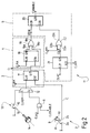
- the circuit 1, comprises a mechanical contactor 2, a sampling circuit 3, a state change detector 4 and a time evaluation circuit 5.
- the mechanical contactor 2 comprises a fixed blade 2a and a movable blade 2b which, at rest, do not touch.
- the contactor 2 is actuated by a cam 8 which is rotated in one direction (referenced 9) by a shaft.
- the cam also has a finger 10 which, during its movement, actuates the blade 2b so that it comes into contact with the blade 2a and causes the contactor to close.
- the blade 2a is connected to the positive terminal of a power supply, so that, when the contactor 2 is in its closed position, a logic signal C of high level is supplied to the sampling circuit 3. Conversely, when the contactor 2 is in its open position, signal C is at a low logic level.
- the sampling circuit 3 samples the signal C with a frequency which is determined by a clock signal CLKA, and provides at output an output signal C i whose logic level corresponds to the logic level of the signal C at the time of sampling. This signal C i is received by the input of the state change detector 4.
- the detector 4 When the state of the signal C i remains constant, the detector 4 provides a low logic level signal to the time evaluation circuit 5. Under these conditions, the time evaluation circuit 5 provides a high logic signal to one of the inputs of an AND gate 6.
- the clock signal CLKA is supplied to the other input of the AND gate 6, so that the signal C is sampled by the sampling circuit 3 at a determined frequency by the CLKA clock signal.
- the detection of a change in the state of the signal C i causes the detector 4 to send a logic signal of high level to the time evaluation circuit 5.
- a low level logic signal is supplied to one of the inputs of AND gate 6, so as to prevent the transmission of CLKA clock pulses to the sampling circuit 3 and thus to block the sampling of signal C.
- the time evaluation circuit 5 supplies this low level logic signal to the input of the AND gate 6 for a period of time equal to the theoretical closing time of the contactor 2.
- This period of time can, for example, be determined by a counter integrated in the time evaluation circuit 5. This counter starts counting at the moment when the high logic signal produced by the detector 4 is initially detected and is incremented with a frequency determined by a clock signal CLKM .
- the time evaluation circuit 5 again supplies a high level logic signal to said input of AND gate 6, so as to allow the transmission of pulses supplied by the time base signal CLKA to sampling circuit 3 for allow the resumption of the sampling of signal C.
- the state of signal C i is therefore kept constant during the theoretical closing period and the signal is not affected by accidental opening of the contact blades 2a and 2b produced for example by shocks or bad contacts.
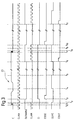
- FIG. 2 represents a particular embodiment of the circuit of the present invention in accordance with the block diagram of FIG. 1, and we will simultaneously refer to the graphs of the evolution of the signals over time represented at FIG. 3.
- FIG. 2 represents a circuit 11 comprising the mechanical contactor 2, the sampling circuit 3, the change of state detector 4, the time evaluation circuit 5 and the AND gate 6 already described with reference in FIG. 1.
- the circuit 11 also includes a multiplexer 12 and a second mechanical contactor 13 actuated by a crown 14.
- the contactor 13 comprises a fixed blade 15 and a movable blade 16 which, at rest, do not touch.
- the contact blades 15 and 16 are brought into contact with one another when the crown 14 is placed in its position for setting the time, and return to their open position when the crown 14 is returned to its position normal running.
- the blade 15 is connected to the positive terminal of a voltage source, so that when the contactor 13 is in its closed position, a high level logic signal is sent to the multiplexer 12, and that when the contactor 13 is in its open position, the signal sent is of low logic level.
- the sampling circuit 3 comprises a D type flip-flop referenced 17 whose input D17 is connected to the contact blade 7 of the contactor 2.
- the flip-flop 17 has its time base input CL17 connected to the output of the miltiplexer 12. Under these conditions, it is therefore the signal supplied by the multiplexer 12 which determines the frequency with which the signal supplied to the input D17 of the flip-flop 17 is sampled.
- a clock signal CLKB is connected to one of the inputs I 1 of the multiplexer 12.
- Another clock signal which is produced by the combination at the AND gate 6 of the clock signal CLKA and the control signal CLENABLE sampling is supplied to the other input I 2 of the multiplexer 12.
- the state change detector 4 comprises another type D flip-flop referenced 18 and an exclusive gate (XOR) 19.
- the flip-flop 18 is connected by its input D18 to the output Q17 of flip-flop 17, and its input d CL18 is powered by the CLKA clock signal.
- the output Q18 of the flip-flop 18 is connected to one of the inputs 19a of the gate XOR 19.
- the other input 19b of the gate XOR 19 is connected to the input D18 of the flip-flop 18.
- the input D18 and the output Q18 of the flip-flop 18 will both be in the same logic state.
- the XOR gate 19 will therefore provide a low level logic signal at its output 19c.
- the output 19c will send, during one of the cycles of the time base signal CLKA, a high level logic pulse to the time evaluation circuit 5.
- the time evaluation circuit 5 comprises an RS 20 flip-flop, a counter 21 and an OR gate 22.
- the RS 20 flip-flop has its reset input R20 connected to the output 19c of the XOR gate 19, so that the the high logic level pulse emitted by the detector 4 produces a reset of the flip-flop RS 20 and causes the output Q20 to go to a low logic level.
- the CLENABLE signal is produced by the Q20 output.
- Counter 21 has a reset input R21 which, when a high level logic signal is supplied to it, resets counter 21 to zero.
- a time base input CL21 is further provided for determining the frequency with which the counter 21 increments when it is in operation.
- the counter 21 also includes an output Q21 which provides a high level logic signal to an input 22a of the OR gate 22 when the counter 21 has been incremented by a determined number of units.
- the output of the multiplexer 12 supplies a time base signal CLKM to the other input 22b of the OR gate 22 and to the reset input 21 of the counter 21.
- circuit 11 when the time is reset will now be described.
- the contactor 13 closes and a high level logic signal is sent to the multiplexer.
- the clock signal CLKB is thus supplied by the output of the multiplexer 12 to the time base input CL17 of the flip-flop 17. In this position, the crown 14 can be turned in one direction to cause rotation of cam 8 in direction 9.
- the cam 8 rotates slowly enough that the contactor 8 remains ideally closed for a period of the order of 30 minutes.
- the rotation of the cam is controlled by the crown 14 and can therefore be much faster. Since under these conditions it is necessary to have a high sampling frequency to sample the signal C produced by the contactor 2, the clock signal CLKB, which determines this sampling frequency, must be of high frequency, and can be around 500 samples per second.
- the contactor 2 When the cam 8 is in the position shown in FIG. 2, the contactor 2 is open and a low level logic signal is supplied to the input D17 of the flip-flop 17.
- the low logic level of this signal C is read by the flip-flop 17 during each falling blank of the clock signal CLKB and supplied at its output Q17.
- the cam 8 When the cam 8 is turned to a position where its finger 10 holds the contact blades 2a and 2b together, the signal C emitted to the input D17 goes to its high level.
- the high level logic signal is read by the flip-flop 17 and transmitted by its output Q17.
- the output Q17 provides the signal C i which is used to indicate the state of the contactor 2.
- the detector 4 and the time evaluation circuit 5 are activated by the change in the state of the signal C, but this operation has no effect on the sampling circuit 3.
- the operation of the circuit 11 in normal operating mode will now be described.
- the contactor 13 opens, which causes the multiplexer 12 to be powered by a signal low level logic.
- the CLENABLE signal is high.
- the clock signal CLKA is, under these conditions, supplied by the output of the AND gate 6 and transmitted by the multiplexer 12 to the time base input CL17, so that the signal C is sampled at the frequency CLKA clock signal.
- the contactor 2 When the signal C is sampled at the instant t 2 , the contactor 2 has changed state and consequently a signal of high logic level is supplied to the input D17.
- the output Q17, and therefore the signal C i pass to their high level and a high level signal is therefore supplied to the input 19b of the gate XOR 19. Since the output Q18 will not go to its high level before the next falling blank of the clock signal CLKA, the output 19c of the gate XOR (referenced by the indication EDGE in FIG. 2) also goes to its high level at time t 3 and for the duration of a clock period.
- the clock signal CLKA can have a period of approximately 1 minute, so that, for example, a shock which would cause the closing of the blades 2a and 2b before the instant t 0 is unlikely to occur. at the time when signal C is sampled.
- the anti-rebound circuits of the prior art which have been described in the introduction pages can be used in other embodiments of the sampling circuit 3 to detect voluntary openings and / or closings of the contactor 2.
- the time during which the signal C remains unsampled is determined by the counter 21 and can correspond to the theoretical closing time of the contactor 2. In the case where the contactor 2 is used in an analog electronic watch in which it is closed by an actuated cam by the watch's hour canon, this time should be between 26 and 30 minutes.
- the counter 21 is reset to zero during each falling blank of the signal CLKM.
- the low logic state of the signal CLKM from the instant t 3 allows the counter 21 to count a predetermined number of changes of state of the signal CLKM, as represented at times t 4 and t 5 , and to supply a high level logic pulse at its output Q21 (referenced COUT in FIG.
- the pulse provided by the Q21 output is sent via the OR gate 22 to the "set" input S20 of the flip-flop RS 20, so that the CLENABLE signal supplied by the Q20 output returns to a state high logic.
- the clock signal CLKA can now be sent via the AND gate 6 and the multiplexer 12 to the time base input CL17, so that from time t 6 the signal CLKM has to again the same form as the time base signal CLKA and that the signal C is therefore again sampled during each falling blank of the signal CLKM.
- the cam 8 has rotated by an angle sufficient for the contact blades 2a and 2b to start to separate.
- the rebounds between the blades 2a and 2b continue to occur until time t 8 , after which the blades remain permanently separated.
- the time which elapses between times t 7 and t 8 can be of the order of one to two minutes. Consequently, the signal C returns to its low logic level.
- this low signal is read by the flip-flop 17.
- the low level of signal C is transferred to output Q17, so that signal C i also goes to its low level.
- a change in the state of the output Q17 results in a difference between the states of the two inputs 19a and 19b of the gate XOR 19 which lasts during one cycle of the signal CLKA. Consequently, a high logic level pulse is supplied to the reset input R20 of the flip-flop RS 20. This causes the CLENABLE signal to pass to its low level, and again blocks reception of the CLKA signal by the flip-flop 17, and also the sampling of the signal C during a period determined by the counter 21.
- the output Q21 produces a pulse which is sent to the set input S20 to return the CLENABLE signal to its high logic level and allow resumption of the signal C sampling.
- the change in the state of the signal C i (FIG. 3) at time t 10 results from an intentional opening of the contactor 2. However, such a change can also be caused by a bad contact after time t 6 .
- the detection of this bad contact will cause the sampling of signal C to be interrupted during the predetermined time, determined by the counter 21, and thus the signal C i will be at its low level during this period.
- the signal C i has already provided a well-defined signal representative of the closure of the contactor 2 between the instant t 3 and the instant t 6 and this parasitic switching will therefore have no effect on the circuit 11.
- the period going from the instant t 6 which represents the end of the theoretical closing time of the contactor 2, and the instant t 7 which represents the end of the real closing time of the contactor 2, is sufficiently short compared to the time during which the signal C ceases to be sampled, to prevent the signal C i from going to its high logic level before the instant t 8 .
- the sampling of signal C does not stop when a watch using circuit 11 is set to the time.
- a sampling interruption may be desirable.
- the clock signal CLKB can be connected to an input of another AND gate, the output of which is connected to the input I1 of the multiplexer 12.
- Another time evaluation circuit is provided to receive the pulses produced by the output 19c of the detector 4, and to supply a low logic level signal to the other input of the additional AND gate so as to prevent the sampling of the signal C for another predetermined duration. If the clock signal CLKB has a period of 20 ms, this period can be of the order of 100 ms.
Landscapes
- Physics & Mathematics (AREA)
- General Physics & Mathematics (AREA)
- Electric Clocks (AREA)
- Electromechanical Clocks (AREA)
- Measurement Of Unknown Time Intervals (AREA)
Applications Claiming Priority (2)
| Application Number | Priority Date | Filing Date | Title |
|---|---|---|---|
| CH820/93A CH684622B5 (fr) | 1993-03-18 | 1993-03-18 | Circuit pour supprimer les effets de rebonds d'un contacteur et montre comprenant un tel circuit. |
| CH820/93 | 1993-03-18 |
Publications (2)
| Publication Number | Publication Date |
|---|---|
| EP0616272A1 EP0616272A1 (fr) | 1994-09-21 |
| EP0616272B1 true EP0616272B1 (fr) | 1997-07-30 |
Family
ID=4195956
Family Applications (1)
| Application Number | Title | Priority Date | Filing Date |
|---|---|---|---|
| EP94103849A Expired - Lifetime EP0616272B1 (fr) | 1993-03-18 | 1994-03-12 | Circuit pour supprimer les effets de rebonds durant l'ouverture ou la fermeture d'un contacteur dans une montre |
Country Status (7)
| Country | Link |
|---|---|
| US (1) | US5500836A (enExample) |
| EP (1) | EP0616272B1 (enExample) |
| JP (1) | JP3507123B2 (enExample) |
| CH (1) | CH684622B5 (enExample) |
| DE (1) | DE69404515T2 (enExample) |
| HK (1) | HK1001742A1 (enExample) |
| TW (1) | TW271468B (enExample) |
Families Citing this family (3)
| Publication number | Priority date | Publication date | Assignee | Title |
|---|---|---|---|---|
| US7391241B2 (en) * | 2004-11-15 | 2008-06-24 | Texas Instruments Incorporated | Bidirectional deglitch circuit |
| US7847614B2 (en) * | 2007-05-30 | 2010-12-07 | Kyocera Corporation | Switch noise reduction device and method using counter |
| JP7013044B2 (ja) | 2020-06-25 | 2022-01-31 | 有限会社タクショー | 鋼板用クリーナ装置 |
Family Cites Families (6)
| Publication number | Priority date | Publication date | Assignee | Title |
|---|---|---|---|---|
| GB1500406A (en) * | 1974-08-14 | 1978-02-08 | Seiko Instr & Electronics | Switching circuits |
| US4138613A (en) * | 1974-08-14 | 1979-02-06 | Kabushiki Kaisha Daini Seikosha | Switching circuit |
| JPS51115869A (en) * | 1975-04-03 | 1976-10-12 | Seiko Instr & Electronics Ltd | Time correction device of electronic clock |
| JPS54135573A (en) * | 1978-03-13 | 1979-10-20 | Seiko Epson Corp | Time correction system |
| JPS5575351A (en) * | 1978-12-01 | 1980-06-06 | Hitachi Denshi Ltd | Input line switching circuit |
| DE3767691D1 (de) * | 1986-12-03 | 1991-02-28 | Ebauchesfabrik Eta Ag | Schaltung zur formung des von einem kontakt produzierten signals. |
-
1993
- 1993-03-18 CH CH820/93A patent/CH684622B5/fr not_active IP Right Cessation
-
1994
- 1994-02-08 TW TW083101077A patent/TW271468B/zh active
- 1994-03-12 DE DE69404515T patent/DE69404515T2/de not_active Expired - Lifetime
- 1994-03-12 EP EP94103849A patent/EP0616272B1/fr not_active Expired - Lifetime
- 1994-03-14 US US08/213,143 patent/US5500836A/en not_active Expired - Lifetime
- 1994-03-18 JP JP07293794A patent/JP3507123B2/ja not_active Expired - Fee Related
-
1998
- 1998-01-26 HK HK98100680A patent/HK1001742A1/xx not_active IP Right Cessation
Also Published As
| Publication number | Publication date |
|---|---|
| TW271468B (enExample) | 1996-03-01 |
| EP0616272A1 (fr) | 1994-09-21 |
| DE69404515T2 (de) | 1998-02-26 |
| JPH06300867A (ja) | 1994-10-28 |
| CH684622B5 (fr) | 1995-05-15 |
| JP3507123B2 (ja) | 2004-03-15 |
| DE69404515D1 (de) | 1997-09-04 |
| CH684622GA3 (fr) | 1994-11-15 |
| HK1001742A1 (en) | 1998-07-03 |
| US5500836A (en) | 1996-03-19 |
Similar Documents
| Publication | Publication Date | Title |
|---|---|---|
| EP0143279A1 (fr) | Montre pourvue d'un affichage analogique et d'un affichage numérique | |
| EP1081563A1 (fr) | Montre du type montre-bracelet | |
| CH686332B5 (fr) | Pièce d'horlogerie mué par une source d'énergie mécanique et régulée par un circuit électronique. | |
| EP0806710A1 (fr) | Stabilisation d'un circuit électronique de régulation du mouvement mécanique d'une piéce d'horlogerie | |
| EP0621703B1 (fr) | Procédé de récupération d'horloge et de synchronisation pour la réception d'informations transmises par un réseau ATM et dispositif de mise en oeuvre du procédé | |
| WO2018015146A1 (fr) | Mecanisme d'echappement | |
| EP0616272B1 (fr) | Circuit pour supprimer les effets de rebonds durant l'ouverture ou la fermeture d'un contacteur dans une montre | |
| EP1798611A1 (fr) | Pièce d'horlogerie comportant un mécanisme de sonnerie à déclenchement instantané | |
| EP0064023B1 (fr) | Dispositif de mise à l'heure pour montre électronique | |
| EP0060806B1 (fr) | Procédé pour réduire la consommation d'un moteur pas-à-pas et dispositif pour la mise en oeuvre de ce procédé | |
| EP0274035B1 (fr) | Circuit de mise en forme du signal produit par un contact | |
| EP0064025B1 (fr) | Montre électronique à organe de commande fixe | |
| EP0135104B1 (fr) | Procédé et dispositif de commande d'un moteur pas-à-pas | |
| EP1798610A1 (fr) | Pièce d'horlogerie comportant un mécanisme de sonnerie à un seul cliquet | |
| CH688950B5 (fr) | Dispositif de synchronisation d'un affichage analogique avec un compteur électronique dans une pièce d'horlogerie. | |
| CH691090A5 (fr) | Montre comportant des moyens de détection de l'insuffisance de la source d'alimentation. | |
| EP1521364B1 (fr) | Procédé et dispositif pour le filtrage de signaux produits par un accéléromètre de type piézo-électrique, et application à un objet portatif tel qu'une montre | |
| EP0027250A1 (fr) | Pièce d'horlogerie avec affichage de la seconde sur demande | |
| EP0203330A1 (fr) | Pièce d'horlogerie électronique comprenant un détecteur de fin de vie de la source de tension | |
| EP0171782B1 (fr) | Pièce d'horlogerie électronique avec possibilité de correction de l'indication des secondes | |
| EP3779611B1 (fr) | Montre électromécanique | |
| EP0006384A1 (fr) | Dispositif de synchronisation à partir d'un signal numérique reçu et système de transmission comportant un tel dispositif | |
| CH714728A2 (fr) | Mécanisme de sonnerie pour mouvement horloger. | |
| EP0875807A1 (fr) | Pièce d'horlogerie électronique alimentée par un générateur entraíné par une source d'énergie mécanique | |
| EP0484770B1 (fr) | Procédé de commande d'un moteur pas à pas et dispositif pour la mise en oeuvre de ce procédé |
Legal Events
| Date | Code | Title | Description |
|---|---|---|---|
| PUAI | Public reference made under article 153(3) epc to a published international application that has entered the european phase |
Free format text: ORIGINAL CODE: 0009012 |
|
| AK | Designated contracting states |
Kind code of ref document: A1 Designated state(s): DE FR GB NL |
|
| 17P | Request for examination filed |
Effective date: 19941004 |
|
| 17Q | First examination report despatched |
Effective date: 19960306 |
|
| GRAG | Despatch of communication of intention to grant |
Free format text: ORIGINAL CODE: EPIDOS AGRA |
|
| GRAH | Despatch of communication of intention to grant a patent |
Free format text: ORIGINAL CODE: EPIDOS IGRA |
|
| GRAH | Despatch of communication of intention to grant a patent |
Free format text: ORIGINAL CODE: EPIDOS IGRA |
|
| GRAA | (expected) grant |
Free format text: ORIGINAL CODE: 0009210 |
|
| AK | Designated contracting states |
Kind code of ref document: B1 Designated state(s): DE FR GB NL |
|
| REF | Corresponds to: |
Ref document number: 69404515 Country of ref document: DE Date of ref document: 19970904 |
|
| GBT | Gb: translation of ep patent filed (gb section 77(6)(a)/1977) |
Effective date: 19970925 |
|
| PLBE | No opposition filed within time limit |
Free format text: ORIGINAL CODE: 0009261 |
|
| STAA | Information on the status of an ep patent application or granted ep patent |
Free format text: STATUS: NO OPPOSITION FILED WITHIN TIME LIMIT |
|
| 26N | No opposition filed | ||
| REG | Reference to a national code |
Ref country code: GB Ref legal event code: IF02 |
|
| PGFP | Annual fee paid to national office [announced via postgrant information from national office to epo] |
Ref country code: GB Payment date: 20050225 Year of fee payment: 12 |
|
| PG25 | Lapsed in a contracting state [announced via postgrant information from national office to epo] |
Ref country code: GB Free format text: LAPSE BECAUSE OF NON-PAYMENT OF DUE FEES Effective date: 20060312 |
|
| GBPC | Gb: european patent ceased through non-payment of renewal fee |
Effective date: 20060312 |
|
| PGFP | Annual fee paid to national office [announced via postgrant information from national office to epo] |
Ref country code: NL Payment date: 20110225 Year of fee payment: 18 |
|
| PGFP | Annual fee paid to national office [announced via postgrant information from national office to epo] |
Ref country code: FR Payment date: 20110412 Year of fee payment: 18 Ref country code: DE Payment date: 20110308 Year of fee payment: 18 |
|
| REG | Reference to a national code |
Ref country code: NL Ref legal event code: V1 Effective date: 20121001 |
|
| REG | Reference to a national code |
Ref country code: FR Ref legal event code: ST Effective date: 20121130 |
|
| PG25 | Lapsed in a contracting state [announced via postgrant information from national office to epo] |
Ref country code: FR Free format text: LAPSE BECAUSE OF NON-PAYMENT OF DUE FEES Effective date: 20120402 |
|
| REG | Reference to a national code |
Ref country code: DE Ref legal event code: R119 Ref document number: 69404515 Country of ref document: DE Effective date: 20121002 |
|
| PG25 | Lapsed in a contracting state [announced via postgrant information from national office to epo] |
Ref country code: NL Free format text: LAPSE BECAUSE OF NON-PAYMENT OF DUE FEES Effective date: 20121001 |
|
| PG25 | Lapsed in a contracting state [announced via postgrant information from national office to epo] |
Ref country code: DE Free format text: LAPSE BECAUSE OF NON-PAYMENT OF DUE FEES Effective date: 20121002 |