EP0615281B1 - Wafer release method and apparatus - Google Patents
Wafer release method and apparatus Download PDFInfo
- Publication number
- EP0615281B1 EP0615281B1 EP94301606A EP94301606A EP0615281B1 EP 0615281 B1 EP0615281 B1 EP 0615281B1 EP 94301606 A EP94301606 A EP 94301606A EP 94301606 A EP94301606 A EP 94301606A EP 0615281 B1 EP0615281 B1 EP 0615281B1
- Authority
- EP
- European Patent Office
- Prior art keywords
- wafer
- electrodes
- support
- treatment apparatus
- polarity
- Prior art date
- Legal status (The legal status is an assumption and is not a legal conclusion. Google has not performed a legal analysis and makes no representation as to the accuracy of the status listed.)
- Expired - Lifetime
Links
Images



Classifications
-
- H—ELECTRICITY
- H10—SEMICONDUCTOR DEVICES; ELECTRIC SOLID-STATE DEVICES NOT OTHERWISE PROVIDED FOR
- H10P—GENERIC PROCESSES OR APPARATUS FOR THE MANUFACTURE OR TREATMENT OF DEVICES COVERED BY CLASS H10
- H10P72/00—Handling or holding of wafers, substrates or devices during manufacture or treatment thereof
- H10P72/70—Handling or holding of wafers, substrates or devices during manufacture or treatment thereof for supporting or gripping
- H10P72/72—Handling or holding of wafers, substrates or devices during manufacture or treatment thereof for supporting or gripping using electrostatic chucks
- H10P72/722—Details of electrostatic chucks
-
- H—ELECTRICITY
- H10—SEMICONDUCTOR DEVICES; ELECTRIC SOLID-STATE DEVICES NOT OTHERWISE PROVIDED FOR
- H10P—GENERIC PROCESSES OR APPARATUS FOR THE MANUFACTURE OR TREATMENT OF DEVICES COVERED BY CLASS H10
- H10P72/00—Handling or holding of wafers, substrates or devices during manufacture or treatment thereof
- H10P72/06—Apparatus for monitoring, sorting, marking, testing or measuring
- H10P72/0606—Position monitoring, e.g. misposition detection or presence detection
-
- H—ELECTRICITY
- H10—SEMICONDUCTOR DEVICES; ELECTRIC SOLID-STATE DEVICES NOT OTHERWISE PROVIDED FOR
- H10P—GENERIC PROCESSES OR APPARATUS FOR THE MANUFACTURE OR TREATMENT OF DEVICES COVERED BY CLASS H10
- H10P72/00—Handling or holding of wafers, substrates or devices during manufacture or treatment thereof
- H10P72/70—Handling or holding of wafers, substrates or devices during manufacture or treatment thereof for supporting or gripping
- H10P72/72—Handling or holding of wafers, substrates or devices during manufacture or treatment thereof for supporting or gripping using electrostatic chucks
Definitions
- the present invention concerns an electrostatic clamp for holding a semiconductor wafer against a wafer support and more particularly to a method and apparatus for controlling operation of such a clamp.
- U.S. Patent No. 5,103,367, entitled Electrostatic Chuck Using A.C. Field Excitation relates to a mechanism for holding semiconductor wafers in contact with a support during treatment of the wafers.
- the electrostatic chuck has three electrodes where two electrodes define a substantially planar surface and are embedded within a thin dielectric film. These two electrodes are excited by a low-frequency (approximately 200 hertz) A.C. supply to produce sign wave fields of controlled amplitude and phase.
- the third electrode accesses a shield electrode that serves as a reference point for the other two electrodes.
- By controlled rates of voltage application and removal low-voltage gradients are obtained on the wafer support. This results in no retentive forces between the dielectric medium and the wafer.
- a low alternating current amplitude excitation of the chuck enables capacitative current sensing of the relative positions of the wafers and the dielectric film enabling simple control of voltage application to the electrodes.
- EP-A-0 460 955 relates to an apparatus for electrostatically clamping a semiconductor wafer.
- Conductive wires are stretched across the surface of a supporting platen and electrically insulated therefrom.
- a bi-polar square wave voltage is applied between the wires during clamping.
- FR-A-2 676 603 describes an electrostatic chuck for a wafer. Wafers are gripped through application of a high voltage. Release of the wafer is obtained while modulating the drive waveform and reducing the voltage level to cause the wafer to vibrate until the wafer is released.
- a common problem associated with electrostatic clamping is that the wafer may not release from the clamp when the holding voltage that is applied to the clamp is turned off. There are several factors which can contribute to this residual clamping force.
- An embodiment of the present invention concerns method and apparatus for handling a semiconductor wafer before and after ion beam treatment of the wafer.
- the semiconductor wafer Prior to treatment, the semiconductor wafer is secured to a wafer support by creating an electrostatic attraction between the wafer and the support.
- the wafer is next typically moved to a treatment station and then returned to a loading station and removed from the support.
- the wafer and wafer support attract each other due to mutual electrostatic attraction.
- a power supply biases the electrodes to create this electrostatic attraction.
- the output polarity of the power supply is switched at a controlled rate to reduce the attraction between the wafer and the wafer support. This allows the wafer to be removed from its support by mechanical wafer handling apparatus known in the prior art.
- the controlled switching can be accompanied by a gradual reduction in amplitude of the potential difference applied across the support electrodes. By diminishing the attraction between the wafer and support, the wafer can be moved without damage, thereby increasing efficiency of the ion implanter.
- the support can be defined as multiple capacitors in series. Different capacitors demonstrate different dielectric constants from different material layers. All capacitors cannot be fully discharged with by simply shorting the wafer support since the discharge current will stop flowing once a certain equilibrium is reached internally (one capacitor becomes a charging source to another during the process). Practice of the invention keeps up sufficient discharge current until the remaining charge is negligible.
- a decayed amplitude in bias voltage can be approximated by applying frequency modulation -- switching voltage polarity of the power supply (across the two support electrodes) with a variable frequency from low to high.
- This technique is based upon the fact that the capacitors are not ideal, which have effectively “lossy” dielectric constants due to the elastomer material of the wafer support. This "exercising" the capacitors causes the dissipation of the stored energy.
- one object of the invention is an ion implantation apparatus and method for facilitating wafer handling while maintaining control over the wafer. This is most preferably accomplished by a wafer release apparatus and method constructed and performed in accordance with the disclosed and claimed invention.
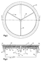
- the drawings illustrate a clamp assembly 10 for supporting and holding a semiconductor wafer 12 (Fig. 3) for processing.
- the clamp assembly 10 includes a backing plate 14 which is preferably formed of alumina or molybdenum, a base member 16 also formed of alumina, a dielectric layer 18 of glass, and a dielectric layer 20 of alumina. Electrodes 22, 24 are interposed between the glass layer 18 and the dielectric layer 20 and a heating element 26 is interposed between the glass layer and the base member 16.
- a gas fitting 28 extends through the chuck assembly opening into the interface between the wafer and the layer 20 to provide gas conduction cooling between the wafer and the chuck as described in U.S. Patent No. 4,261,762.
- a gas distribution groove 29 is formed in the top surface of layer 20 to aid in the distribution of the gas.
- the base member 16 defines a manifold having a channel 30 for the flow of a cooling fluid.
- the channel is formed as a spiral; however, it can also follow a meandering path or it can be a series of interconnected channels.
- the channels are closed to define an enclosed conduit or conduits by means of the backing plate 14, which is sealed against the manifold. Openings are provided in the backing plate for a coolant inlet fitting 32 and a coolant outlet fitting 34. Since the present chuck assembly is intended to perform under a wide range of temperature conditions, the cooling medium flowing through the manifold can be either a liquid or a gas, depending on the application.
- the dielectric layer 20 is preferably formed of a thin (about .25 mm) layer of high purity (99.5%) alumina.
- the electrodes 22 and 24 are then formed on the bottom (as seen in Fig. 2) surface of the dielectric layer, preferably by screen printing a paste of powdered copper aluminum or silver palladium metals and glass frit onto the dielectric layer and then firing it at about 700°C. As shown in Figure 2, the electrodes are essentially half circular in plan view.
- the heating element 26 is formed by screen printing a paste of powdered tungsten and glass frit onto the manifold in the form of a continuous meander, the geometry of the meander preferably being as shown in Figure 3 to provide a higher heater power density at the outer edge to optimize temperature uniformity across the chuck.
- the layer 20 is bonded to the manifold.
- the backing plate 14 is furnace brazed or sealed by means of a sealing glass to the bottom of the manifold 16.
- access holes 36, 38 are formed through the backing plate 14, the manifold 16 and the dielectric layer 18 for a first conductor 40 connected to the electrode 22 and for a second conductor 42 connected to the electrode 24.
- the conductors 40, 42 are attached to the electrodes by brazing or other convenient methods such as by providing spring contacts engageable with the electrodes and are connected to a power supply 44 (Fig. 1) which provides a signal of about 3 kilovolts DC to create the electrostatic clamping force to a semiconductor wafer 12 placed on the surface of the dielectric layer 20.
- the power supply 44 includes two modules 44a, 44b which are coupled together to provide a bi-polar output.
- Access holes 46, 48 are also formed through the backing plate 14 and the manifold 16 for a third conductor 50 attached to one terminal of heating element 26 also by brazing or the like, and fourth conductor 52 similarly attached to the other terminal of heating element 26 to connect the heating element to a second power source 54, typically operating at 120 volts.
- the access holes 36, 38 and the hole for the gas fitting 28 are machined into the structure with the holes 36, 38 sealed with sealing glass and the fitting bonded into its hole with sealing glass.
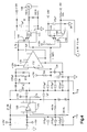
- two inputs 110, 112 from the electrodes 22, 24 are coupled to a capacitive sense circuit 114.
- a capacitance across these two inputs 110, 112 corresponds to the capacitance between the electrodes 22, 24 and is influenced by the presence of a wafer as well as the voltage applied to the electrodes.
- These two inputs are coupled to an operational amplifier 120 within an integrated circuit 122.
- the integrated circuit is a commercially available circuit designated LF 356 and can be obtained from National Semiconductor.
- the operational amplifier 120 generates an output which oscillates with a frequency directly related to the capacitance between the inputs 110, 112.
- the oscillating output signal from the operational amplifier 120 varies between 0 and 5 volts.
- This signal is shaped and then coupled to a comparator amplifier 130 having a reference input 132 defined by a zener diode 134 at approximately 5 volts.
- the comparator amplifier 130 creates a square wave signal output having a 50% duty cycle having an ON period that varies depending on the sensed capacitance. For a 4-inch circular diameter wafer, this period is approximately 20 microseconds with no wafer in place, 30 microseconds with a wafer placed on the layer 20, and 40 microseconds with the wafer in place and a clamping voltage (approximately 3 kilovolts) applied to the electrodes by the power supply 44.
- An output from the comparator amplifier 130 turns on and off light-emitting diodes 140, 142 which are optoisolated from corresponding photodetectors.
- a top photodetector 144 is used for diagnostic purposes and an output 148 from the detector 144 can be coupled to an oscilloscope, for example, for monitoring frequency changes with capacitance.
- a second photodetector 146 generates a signal which turns on and off a transistor 150 which is coupled to an analog switch 152 (Fig. 4A).
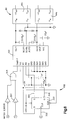
- This analog switch 152 has in input (IN) coupled to the collector of the transistor 150.
- outputs (S1, S2) of the switch 152 sequentially change state from ground to 8 volts in accordance with the square wave frequency output from the comparator 130.
- the output from the analog switch 152 is integrated by a resistor, capacitor circuit 154 so that the input to a non-inverting input 160 of an operational amplifier 162 is a voltage level directly related to the capacitance sensed by the circuit 114.
- This operational amplifier 162 operates as a voltage follower so that an output 164 designated FVOUT is a DC output signal directly related to sensed capacitance.
- This DC output signal is used by an implanter control system 250 (Fig. 6) to monitor performance of the system.
- the wafer handler for depositing a wafer onto the chuck is activated in response to an appropriate no wafer condition being sensed. Once the wafer is sensed, an output from the control circuit 250 activates the DC power supply 44 to energize the electrodes 22, 24 causing an electrostatic attraction between the clamp and the wafer.
- FIG. 5 discloses a power supply circuit 200 for generating voltages appropriate for the capacitance monitoring circuit 114.
- Two inputs 210, 212 at the left of Figure 5 provide a voltage which energizes a light-emitting diode 213. This voltage produces a 12-volt signal due to the voltage clamping operation of a zener diode 214.
- the 12-volt signal is then coupled to integrated circuit voltage regulators 216, 218 for producing +8 and +5 volts.
- a DC to DC converter 220 provides plus and minus 15-volt signals. These voltages are applied to the circuitry of Figures 4, 4A for providing the capacitance monitoring capability.
- the implanter control system 250 of Figure 6 interfaces with a wafer release circuit 300 depicted in Figures 7 and 8 that activates the power supply 44 with the bi-polar output configuration.
- the circuit 300 includes a logic driver circuit 310 having two outputs OUT1, OUT2 coupled to two power supply modules 44a, 44b.
- the power supply modules are preferably MC-30 power supplies commercially available from Gamma High Voltage of Ormond Beach, Florida.
- Two inputs IN1, IN2 control the outputs OUT1, OUT2.
- IN1 is positive
- the output OUT1 from the logic circuit 310 is positive and acts as a current source so a first power supply module 44a is activated.
- the voltage across the two electrodes mounted to the wafer support is of a first polarity.
- the output designated OUT2 from the logic circuit 310 is positive and acts as a current source and the second switching power supply module 44b is active so the polarity of the voltage across the electrodes is switched.
- the circuit 310 is commercially available from SGS Thompson under part designation L6202.
- one module of the power supply 44 is activated to maintain an electrostatic attraction between wafer and support.
- an ENABLE input 312 to the circuit 310 is high and one or the other of the inputs IN1, IN2 remains positive during ion implantation. This causes a fixed voltage to be applied to the electrodes 22, 24 maintaining electrostatic attraction between the wafer and the support.
- the enable input ENABLE to the circuit 310 remains high, but the two inputs IN1, IN2 are alternately turned on and off by means of the Q and not Q outputs from a flip-flop 320.
- the frequency at which the polarity of the power supply is switched is controlled by an input 322 to the flip-flop 320.
- the flip-flop is configured as a divide-by-two counter so that if the signal at the input has a frequency f, the outputs change state at a frequency of f/2.
- the input 322 to the flip-flop 320 originates from an AND gate 330 having two inputs 332, 334.
- One input 332 to the AND gate 330 depends upon control signal from the controller 250 which is applied across two inputs 340, 342 to an optoisolator 344.
- an input 340 is positive with respect to the input 342
- current flows through a light-emitting diode 344a within the optoisolator, activating a photosensor 344b.
- This generates a low output which is coupled to the input 332.
- the voltage across the two inputs 340, 342 is applied by the controller 250 when the controller has sensed the presence of a wafer on the support and responds to this sensed condition by activating the electrostatic attraction between the wafer and the support.
- the state of the two inputs IN1, IN2 causes one or the other of the modules 44a, 44b to be activated so that a voltage difference is applied to the electrodes within the wafer support. This activates electrostatic attraction between the wafer support and wafer.
- a second input to the AND gate 354 from an invertor 353 receives a hardware generated wafer sense signal derived from the FVOUT signal 164.
- the controller 250 de-activates the electrostatic attraction by providing a control signal to cause the polarity of the voltage applied to the wafer electrodes to change back and forth, thereby dissipating the electrostatic energy between wafer and electrode.
- the output signal from the optoisolator 344 goes high, therefore, assuring one input 332 to the AND gate 330 is also high.
- Two additional controller generated inputs 360, 362 are coupled to a second optoisolator 364.
- this second optoisolator 364 is activated and a low output from the optoisolator is coupled through an invertor 366 and, therefore, goes high.
- This high-input signal is coupled to a first one-shot 370, causing a Q output 372 from the one-shot 370 to go high.
- the not Q output simultaneously goes low and is coupled to the gate 350 for enabling the drive circuit 310.
- the Q output from the one-shot 370 is coupled to a second one-shot 380 which is configured as an oscillator circuit.
- the Q output from this one-shot is fed back to the activation input through an external circuit which causes the second one-shot 380 to oscillate with a predetermined frequency of approximately 20 Hz.
- This causes the input 334 to the AND gate 330 to be pulsed at this frequency.
- the output of the AND gate 330 is coupled to the flip-flop which acts as a divide-by-two counter. This causes the polarity on the electrodes to oscillate back and forth for a time period equal to the output time of the first one-shot 370.
- the Q output from this one-shot de-activates the oscillator one-shot 380 and also removes the enable signal from the circuit 310.
- the controller 250 directly activates the inputs 340, 342 for controlled ON/OFF intervals.
- the junction 322 is low when the input 340 is high.
- the frequency of switching from the circuit 310 is controlled which, in turn, controls the polarity switching of the two power supply modules 44a, 44b.
- Three jumper connections P1, P2, P3 at the input to the one-shot 370 are set depending on whether the controller performs the switching or the combination of one-shot 370 and multivibrator 380 control the switching.
- a jumper across P1 and P2 disables the one-shot 370, and a jumper across P2, P3 enables the one-shot.
- a wafer 12 which is to be processed, is placed upon the surface of the layer 20, and the supply 44 will be energized to apply an electrostatic attractive force between the wafer and the layer 20 sufficient to maintain the wafer in position on the chuck.
- the chuck 10 can then be both rotated and translated to bring the wafer to a wafer treatment station such as an ion implantation chamber.
- the implanter control system 250 (Fig. 6) has a large number of device interfaces which receive inputs from sensors 252 (for example, gauges measuring pressures, voltmeters, encoders measuring mechanical position, and the FVOUT output 164), and send operating commands to mechanical and electrical components 254 (for example, valves, power supplies, robots, and the electrostatic clamp power supply 44).
- sensors 252 for example, gauges measuring pressures, voltmeters, encoders measuring mechanical position, and the FVOUT output 164
- mechanical and electrical components 254 for example, valves, power supplies, robots, and the electrostatic clamp power supply 44.
- the output 164 indicates the wafer's presence and whether it is clamped and provides critical information for these cross checks to implement wafer handling and implantation operations. For example, the assembly 10 would not be rotated into a vertical position unless the wafer was verified to be securely clamped. Similarly, the clamp would not be activated unless the wafer's presence on the clamp was verified.
- the control system 250 has the ability to place the implanter into HOLD (suspend further operation) in order to avoid damage to the machine or to produce wafers.
- a second function of the series of cross checks is to provide an operator interface 260 information about machine status. Specifically, when a cross check fails, an alarm message is generated for display on an operator interface screen, and is recorded in a data log maintained on a disk drive. This information permits an operator to take corrective action to restore normal machine operation.
- the assembly 10 is moved to position the wafer for removal from the support.
- the controller 250 then either signals the one-shot 370 to activate polarity reversal of the power supply 40 or directly switches that polarity at a controlled frequency.
- the electrodes are biased with alternating polarity and release the wafer by reducing electrostatic attraction between the wafer support and the wafer.
- Figure 6 represents current state-of-the-art for control equipment.
- the addition of the capacitive sensing circuit 114 and the wafer release circuit 300 represents an advance in the quality of information available about the status of the wafer on the clamp 10 and the ability to efficiently treat wafers.
Landscapes
- Container, Conveyance, Adherence, Positioning, Of Wafer (AREA)
- Jigs For Machine Tools (AREA)
Description
- The present invention concerns an electrostatic clamp for holding a semiconductor wafer against a wafer support and more particularly to a method and apparatus for controlling operation of such a clamp.
- U.S. Patent No. 5,103,367, entitled Electrostatic Chuck Using A.C. Field Excitation relates to a mechanism for holding semiconductor wafers in contact with a support during treatment of the wafers. The electrostatic chuck has three electrodes where two electrodes define a substantially planar surface and are embedded within a thin dielectric film. These two electrodes are excited by a low-frequency (approximately 200 hertz) A.C. supply to produce sign wave fields of controlled amplitude and phase. The third electrode accesses a shield electrode that serves as a reference point for the other two electrodes. By controlled rates of voltage application and removal, low-voltage gradients are obtained on the wafer support. This results in no retentive forces between the dielectric medium and the wafer. A low alternating current amplitude excitation of the chuck enables capacitative current sensing of the relative positions of the wafers and the dielectric film enabling simple control of voltage application to the electrodes.
- EP-A-0 460 955 relates to an apparatus for electrostatically clamping a semiconductor wafer. Conductive wires are stretched across the surface of a supporting platen and electrically insulated therefrom. In one embodiment, a bi-polar square wave voltage is applied between the wires during clamping.
- FR-A-2 676 603 describes an electrostatic chuck for a wafer. Wafers are gripped through application of a high voltage. Release of the wafer is obtained while modulating the drive waveform and reducing the voltage level to cause the wafer to vibrate until the wafer is released.
- A common problem associated with electrostatic clamping is that the wafer may not release from the clamp when the holding voltage that is applied to the clamp is turned off. There are several factors which can contribute to this residual clamping force.
- First, most dielectrics can exhibit a degree of semipermanent polarization following exposure to an intense electric field. This polarization has the effect of maintaining the clamping force even after the applied voltage is removed. Materials with a high dielectric constant are particularly prone to this effect, and it is exactly such materials which are favored as the dielectric material for a wafer support because their high dielectric constant provides an enhancement of the clamping force.
- Second, stored elastic energy in the clamp can result in a residual clamping force, even were the dielectric a perfect material without any residual polarization. For example, in the case where an elastomer is part of the clamp structure, the capacitance of the clamp becomes voltage dependent. This makes discharge of the series of capacitors which comprise the clamp impossible by simple shorting the voltage supply. Rather, the stored energy must be dissipated in an external circuit. Because the clamp circuitry is not a simply D.C. source but contains capacitance and inductance, simple shorting through an external circuit to extract the stored energy will not work.
- The invention provides an apparatus and method as defined in
claims - As the wafer is being treated, the wafer and wafer support attract each other due to mutual electrostatic attraction. A power supply biases the electrodes to create this electrostatic attraction.
- After the wafer has been treated, the output polarity of the power supply is switched at a controlled rate to reduce the attraction between the wafer and the wafer support. This allows the wafer to be removed from its support by mechanical wafer handling apparatus known in the prior art. The controlled switching can be accompanied by a gradual reduction in amplitude of the potential difference applied across the support electrodes. By diminishing the attraction between the wafer and support, the wafer can be moved without damage, thereby increasing efficiency of the ion implanter.
- It is possible that a residual attraction between wafer and wafer support experienced in prior art wafer treatment systems is caused by charge stored in the wafer support. From review of the structure and construction of the electrostatic clamping, the support can be defined as multiple capacitors in series. Different capacitors demonstrate different dielectric constants from different material layers. All capacitors cannot be fully discharged with by simply shorting the wafer support since the discharge current will stop flowing once a certain equilibrium is reached internally (one capacitor becomes a charging source to another during the process). Practice of the invention keeps up sufficient discharge current until the remaining charge is negligible.
- A decayed amplitude in bias voltage can be approximated by applying frequency modulation -- switching voltage polarity of the power supply (across the two support electrodes) with a variable frequency from low to high. This technique is based upon the fact that the capacitors are not ideal, which have effectively "lossy" dielectric constants due to the elastomer material of the wafer support. This "exercising" the capacitors causes the dissipation of the stored energy.
- From the above, it is appreciated that one object of the invention is an ion implantation apparatus and method for facilitating wafer handling while maintaining control over the wafer. This is most preferably accomplished by a wafer release apparatus and method constructed and performed in accordance with the disclosed and claimed invention. This, and other objects, advantages and features of the invention will become better understood from a detailed description of the preferred embodiment of the invention which is described in conjunction with the accompanying drawings.
-
- Figure 1 is a schematic of a power supply, electrostatic clamp assembly and capacitance measuring circuit;
- Figure 2 is a plan view of a wafer support used in an ion implanter;
- Figure 3 is a view as seen from the plane 3-3 in Figure 2;
- Figures 4 and 4A are schematics of a capacitance sensing circuit;
- Figure 5 is a power supply circuit for energizing the sensing circuit of Figures 4 and 4A;
- Figure 6 is a schematic of a control system that utilizes an output of the capacitance sensing circuit of Figures 4 and 4A to control an ion implanter; and
- Figures 7 and 8 are schematics of circuitry for controlling a polarity of an output from the power supply shown in Figure 1
-
- The drawings illustrate a
clamp assembly 10 for supporting and holding a semiconductor wafer 12 (Fig. 3) for processing. Theclamp assembly 10 includes abacking plate 14 which is preferably formed of alumina or molybdenum, abase member 16 also formed of alumina, adielectric layer 18 of glass, and adielectric layer 20 of alumina.Electrodes glass layer 18 and thedielectric layer 20 and aheating element 26 is interposed between the glass layer and thebase member 16. - A
gas fitting 28 extends through the chuck assembly opening into the interface between the wafer and thelayer 20 to provide gas conduction cooling between the wafer and the chuck as described in U.S. Patent No. 4,261,762. Agas distribution groove 29 is formed in the top surface oflayer 20 to aid in the distribution of the gas. - The
base member 16 defines a manifold having achannel 30 for the flow of a cooling fluid. In the preferred embodiment shown, the channel is formed as a spiral; however, it can also follow a meandering path or it can be a series of interconnected channels. The channels are closed to define an enclosed conduit or conduits by means of thebacking plate 14, which is sealed against the manifold. Openings are provided in the backing plate for a coolant inlet fitting 32 and a coolant outlet fitting 34. Since the present chuck assembly is intended to perform under a wide range of temperature conditions, the cooling medium flowing through the manifold can be either a liquid or a gas, depending on the application. - The
dielectric layer 20 is preferably formed of a thin (about .25 mm) layer of high purity (99.5%) alumina. Theelectrodes - The
heating element 26 is formed by screen printing a paste of powdered tungsten and glass frit onto the manifold in the form of a continuous meander, the geometry of the meander preferably being as shown in Figure 3 to provide a higher heater power density at the outer edge to optimize temperature uniformity across the chuck. - Once the
electrodes heating element 26 are fired onto the dielectric layer, thelayer 20 is bonded to the manifold. After the above assembly is complete, thebacking plate 14 is furnace brazed or sealed by means of a sealing glass to the bottom of the manifold 16. - As shown schematically in Figure 3, access holes 36, 38 are formed through the
backing plate 14, the manifold 16 and thedielectric layer 18 for afirst conductor 40 connected to theelectrode 22 and for asecond conductor 42 connected to theelectrode 24. Theconductors semiconductor wafer 12 placed on the surface of thedielectric layer 20. Thepower supply 44 includes twomodules - Access holes 46, 48 are also formed through the
backing plate 14 and the manifold 16 for athird conductor 50 attached to one terminal ofheating element 26 also by brazing or the like, andfourth conductor 52 similarly attached to the other terminal ofheating element 26 to connect the heating element to asecond power source 54, typically operating at 120 volts. Preferably, the access holes 36, 38 and the hole for the gas fitting 28 are machined into the structure with theholes - As seen in Figure 1, two
inputs electrodes capacitive sense circuit 114. A capacitance across these twoinputs electrodes operational amplifier 120 within anintegrated circuit 122. The integrated circuit is a commercially available circuit designated LF 356 and can be obtained from National Semiconductor. - The
operational amplifier 120 generates an output which oscillates with a frequency directly related to the capacitance between theinputs - The oscillating output signal from the
operational amplifier 120 varies between 0 and 5 volts. This signal is shaped and then coupled to acomparator amplifier 130 having areference input 132 defined by azener diode 134 at approximately 5 volts. Thecomparator amplifier 130 creates a square wave signal output having a 50% duty cycle having an ON period that varies depending on the sensed capacitance. For a 4-inch circular diameter wafer, this period is approximately 20 microseconds with no wafer in place, 30 microseconds with a wafer placed on thelayer power supply 44. - An output from the
comparator amplifier 130 turns on and off light-emittingdiodes top photodetector 144 is used for diagnostic purposes and anoutput 148 from thedetector 144 can be coupled to an oscilloscope, for example, for monitoring frequency changes with capacitance. - A
second photodetector 146 generates a signal which turns on and off atransistor 150 which is coupled to an analog switch 152 (Fig. 4A). Thisanalog switch 152 has in input (IN) coupled to the collector of thetransistor 150. As the transistor turns on and off, outputs (S1, S2) of theswitch 152 sequentially change state from ground to 8 volts in accordance with the square wave frequency output from thecomparator 130. - The output from the
analog switch 152 is integrated by a resistor,capacitor circuit 154 so that the input to anon-inverting input 160 of anoperational amplifier 162 is a voltage level directly related to the capacitance sensed by thecircuit 114. Thisoperational amplifier 162 operates as a voltage follower so that anoutput 164 designated FVOUT is a DC output signal directly related to sensed capacitance. This DC output signal is used by an implanter control system 250 (Fig. 6) to monitor performance of the system. The wafer handler for depositing a wafer onto the chuck is activated in response to an appropriate no wafer condition being sensed. Once the wafer is sensed, an output from thecontrol circuit 250 activates theDC power supply 44 to energize theelectrodes - Turning to Figure 5, this figure discloses a
power supply circuit 200 for generating voltages appropriate for thecapacitance monitoring circuit 114. Twoinputs zener diode 214. The 12-volt signal is then coupled to integratedcircuit voltage regulators DC converter 220 provides plus and minus 15-volt signals. These voltages are applied to the circuitry of Figures 4, 4A for providing the capacitance monitoring capability. - The
implanter control system 250 of Figure 6 interfaces with awafer release circuit 300 depicted in Figures 7 and 8 that activates thepower supply 44 with the bi-polar output configuration. Thecircuit 300 includes alogic driver circuit 310 having two outputs OUT1, OUT2 coupled to twopower supply modules logic circuit 310 is positive and acts as a current source so a firstpower supply module 44a is activated. When this happens, the voltage across the two electrodes mounted to the wafer support is of a first polarity. When IN2 is positive, the output designated OUT2 from thelogic circuit 310 is positive and acts as a current source and the second switchingpower supply module 44b is active so the polarity of the voltage across the electrodes is switched. Thecircuit 310 is commercially available from SGS Thompson under part designation L6202. - After a wafer is placed on the
support layer 20, prior to wafer implantation, one module of thepower supply 44 is activated to maintain an electrostatic attraction between wafer and support. To accomplish this, an ENABLE input 312 to thecircuit 310 is high and one or the other of the inputs IN1, IN2 remains positive during ion implantation. This causes a fixed voltage to be applied to theelectrodes - When the wafer is to be released from the support, the enable input ENABLE to the
circuit 310 remains high, but the two inputs IN1, IN2 are alternately turned on and off by means of the Q and not Q outputs from a flip-flop 320. The frequency at which the polarity of the power supply is switched is controlled by aninput 322 to the flip-flop 320. The flip-flop is configured as a divide-by-two counter so that if the signal at the input has a frequency f, the outputs change state at a frequency of f/2. When the Q and not Q outputs switch, a different one of themodules - Turning now to Figure 7, the
input 322 to the flip-flop 320 originates from an ANDgate 330 having twoinputs input 332 to the ANDgate 330 depends upon control signal from thecontroller 250 which is applied across twoinputs optoisolator 344. When aninput 340 is positive with respect to theinput 342, current flows through a light-emittingdiode 344a within the optoisolator, activating aphotosensor 344b. This generates a low output which is coupled to theinput 332. The voltage across the twoinputs controller 250 when the controller has sensed the presence of a wafer on the support and responds to this sensed condition by activating the electrostatic attraction between the wafer and the support. - When a clamp activation voltage is applied by the
controller 250 to theinputs input 332 to the ANDgate 330 goes low causing the output from the ANDgate 330 to go low and maintain the flip-flop 320 in one state (which state is not important during clamping). As seen in Figure 7, this low output signal from theoptoisolator 344 is also applied to a negative ORgate 350 having an output coupled through aninvertor 352 to an AND gate 354 (Figure 8). A low output from theoptoisolator 344 causes the ANDgate 354 output to go high, causing the enable input 312 of thelogic driver circuit 310 to receive an activation signal. The state of the two inputs IN1, IN2 causes one or the other of themodules gate 354 from an invertor 353 receives a hardware generated wafer sense signal derived from theFVOUT signal 164. - Subsequent to ion implantation, the
controller 250 de-activates the electrostatic attraction by providing a control signal to cause the polarity of the voltage applied to the wafer electrodes to change back and forth, thereby dissipating the electrostatic energy between wafer and electrode. - When the
controller 250 de-activates wafer clamping, the output signal from theoptoisolator 344 goes high, therefore, assuring oneinput 332 to the ANDgate 330 is also high. Two additional controller generatedinputs input 360 is more positive than the voltage at theinput 362, this second optoisolator 364 is activated and a low output from the optoisolator is coupled through an invertor 366 and, therefore, goes high. This high-input signal is coupled to a first one-shot 370, causing a Q output 372 from the one-shot 370 to go high. The not Q output simultaneously goes low and is coupled to thegate 350 for enabling thedrive circuit 310. Thus, even though thesignal 340 from the controller is removed, the drive circuit is still enabled. The Q output from the one-shot 370 is coupled to a second one-shot 380 which is configured as an oscillator circuit. The Q output from this one-shot is fed back to the activation input through an external circuit which causes the second one-shot 380 to oscillate with a predetermined frequency of approximately 20 Hz. This causes theinput 334 to the ANDgate 330 to be pulsed at this frequency. As noted above, the output of the ANDgate 330 is coupled to the flip-flop which acts as a divide-by-two counter. This causes the polarity on the electrodes to oscillate back and forth for a time period equal to the output time of the first one-shot 370. After the one-shot 370 times out, the Q output from this one-shot de-activates the oscillator one-shot 380 and also removes the enable signal from thecircuit 310. - In accordance with a second embodiment of the controlled release mechanism of the invention, the
controller 250 directly activates theinputs junction 322 is low when theinput 340 is high. By clocking theinput 340 at a controlled or adjustable rate, the frequency of switching from thecircuit 310 is controlled which, in turn, controls the polarity switching of the twopower supply modules shot 370 are set depending on whether the controller performs the switching or the combination of one-shot 370 and multivibrator 380 control the switching. A jumper across P1 and P2 disables the one-shot 370, and a jumper across P2, P3 enables the one-shot. - In operation, a
wafer 12, which is to be processed, is placed upon the surface of thelayer 20, and thesupply 44 will be energized to apply an electrostatic attractive force between the wafer and thelayer 20 sufficient to maintain the wafer in position on the chuck. Thechuck 10 can then be both rotated and translated to bring the wafer to a wafer treatment station such as an ion implantation chamber. - The implanter control system 250 (Fig. 6) has a large number of device interfaces which receive inputs from sensors 252 (for example, gauges measuring pressures, voltmeters, encoders measuring mechanical position, and the FVOUT output 164), and send operating commands to mechanical and electrical components 254 (for example, valves, power supplies, robots, and the electrostatic clamp power supply 44).
- Within the control system there are programmed a variety of cross checks which must be performed before sending an operating command (for example, the valve to a cryopump cannot be opened unless it is verified that the chamber is already under rough vacuum). The
output 164 indicates the wafer's presence and whether it is clamped and provides critical information for these cross checks to implement wafer handling and implantation operations. For example, theassembly 10 would not be rotated into a vertical position unless the wafer was verified to be securely clamped. Similarly, the clamp would not be activated unless the wafer's presence on the clamp was verified. When a critical cross check fails, thecontrol system 250 has the ability to place the implanter into HOLD (suspend further operation) in order to avoid damage to the machine or to produce wafers. - A second function of the series of cross checks is to provide an
operator interface 260 information about machine status. Specifically, when a cross check fails, an alarm message is generated for display on an operator interface screen, and is recorded in a data log maintained on a disk drive. This information permits an operator to take corrective action to restore normal machine operation. - Once the wafer has been ion treated, the
assembly 10 is moved to position the wafer for removal from the support. Thecontroller 250 then either signals the one-shot 370 to activate polarity reversal of thepower supply 40 or directly switches that polarity at a controlled frequency. The electrodes are biased with alternating polarity and release the wafer by reducing electrostatic attraction between the wafer support and the wafer. - Figure 6 represents current state-of-the-art for control equipment. The addition of the
capacitive sensing circuit 114 and thewafer release circuit 300 represents an advance in the quality of information available about the status of the wafer on theclamp 10 and the ability to efficiently treat wafers.
Claims (15)
- Wafer treatment apparatus for ion implantation of semiconductor wafers, the wafer treatment apparatus comprising:a) a wafer support (14,16,18,20) for supporting a wafer (12) placed thereon and including a first dielectric layer (20) that engages the wafer and two electrodes (22,24);b) a bi-polar output power supply (44) coupled to the two electrodes for energizing the electrodes by providing controlled first and second polarity bias signals of opposite polarity across the electrodes; andc) a control system (250,300) coupled to the power supply including circuitry for securing the wafer to the wafer support by applying a clamping voltage across the electrodes,
wherein said circuitry is designed to apply one of the first and second polarity bias signals as a DC polarity signal across the electrodes thereby electrostatically attracting the wafer to the wafer support during ion implantation,
characterised in that said circuitry is designed to activate polarity reversal and to apply the first and second polarity bias signals to the electrodes at a controlled frequency for a predetermined time interval to reduce the electrostatic attraction of the wafer to the wafer support, after implantation of the wafer is complete. - The wafer treatment apparatus of claim 1 wherein the first dielectric layer is comprised of alumina.
- The wafer treatment apparatus of claim 1 or 2 further including capacitance sense circuitry means (114) for detecting a presence or absence of the wafer on the wafer support by sensing a capacitance between the two electrodes.
- The wafer treatment apparatus of claim 3 wherein the capacitance sense circuitry means is adapted to produce an output signal indicative of the presence of the wafer on the wafer support, the output signal being coupled to the control system such that the electrodes are to be energized only when the output signal indicates a wafer is present on the wafer support.
- The wafer treatment apparatus of claims 3 or 4 wherein the capacitance sense circuitry means (114) is adapted to monitor an attraction produced by the power supply (44) based upon sensed capacitance between the electrodes once a power supply voltage has been applied to the electrodes.
- The wafer treatment apparatus of any of claims 1-5 wherein the wafer support further includes a backing plate (14) a base member (16) and a second dielectric layer (18) disposed between said first dielectric layer and said base member.
- The wafer treatment apparatus of claim 6 wherein the two electrodes are interposed between the first and second dielectric layers.
- The wafer treatment apparatus of claim 6 or 7 including a heating element (26) interposed between the second dielectric layer and the base member.
- The wafer treatment apparatus of any of claims 1-8 wherein the signal applied to the electrodes to secure the wafer to the wafer support is approximately three kilovolts DC.
- The wafer treatment apparatus of any of claims 1-9 wherein the base member defines a manifold having a channel (30) through which cooling fluid is circulated.
- The wafer treatment apparatus of any of claims 1-10 wherein the bi-polar power supply comprises two supply modules (44a,44b) and the control system circuitry includes a logic driver circuit (310) having first and second complementary outputs (OUT1, OUT2), each output coupled to a different one of the bi-polar output power supply modules such that when one of the first and second driver outputs is logic high the supply module coupled thereto applies a signal and the other of the first and second driver outputs is logic low and the supply module (44a,44b) coupled thereto is disabled.
- A wafer handling method for use in treatment of a semiconductor wafer (12) comprising the steps of:a) placing a semiconductor wafer to be treated on a wafer support (14,16,18,20);b) electrostatically attracting the wafer to the support by electrically biasing the wafer support with a voltage signal to create an electrostatic attraction between the semiconductor wafer and the wafer support; andc) treating the wafer while maintaining an electrical bias with a first polarity DC signal to maintain an attraction between the wafer and the wafer support, characterised by the steps of:d) dissipating attraction between the wafer and the wafer support after the treatment of the wafer is complete by applying a second polarity signal to the wafer support that is opposite in polarity to the first polarity DC signal, and then applying alternating signals having the first and second polarities at a controlled frequency for a predetermined time interval to reduce the electrostatic attraction between the wafer and the wafer support.
- The wafer handling method set forth in claim 12 additionally comprising the step of detecting a presence of a wafer on the wafer support prior to treatment of the wafer.
- The wafer handling method set forth in claim 13 wherein the step of detecting a presence of a wafer on the wafer support is performed by sensing a capacitance between two spaced apart electrodes (22,24) coupled to the wafer support.
- The wafer handling method set forth in any of claims 12-14 additionally comprising the step of removing the treated wafer from the wafer support.
Applications Claiming Priority (2)
| Application Number | Priority Date | Filing Date | Title |
|---|---|---|---|
| US08/029,154 US5444597A (en) | 1993-01-15 | 1993-03-10 | Wafer release method and apparatus |
| US29154 | 1993-03-10 |
Publications (2)
| Publication Number | Publication Date |
|---|---|
| EP0615281A1 EP0615281A1 (en) | 1994-09-14 |
| EP0615281B1 true EP0615281B1 (en) | 2000-10-25 |
Family
ID=21847544
Family Applications (1)
| Application Number | Title | Priority Date | Filing Date |
|---|---|---|---|
| EP94301606A Expired - Lifetime EP0615281B1 (en) | 1993-03-10 | 1994-03-08 | Wafer release method and apparatus |
Country Status (8)
| Country | Link |
|---|---|
| US (1) | US5444597A (en) |
| EP (1) | EP0615281B1 (en) |
| JP (1) | JPH077074A (en) |
| KR (1) | KR100304241B1 (en) |
| CN (1) | CN1052112C (en) |
| CA (1) | CA2118619C (en) |
| DE (1) | DE69426163T2 (en) |
| TW (1) | TW312034B (en) |
Cited By (1)
| Publication number | Priority date | Publication date | Assignee | Title |
|---|---|---|---|---|
| DE10214272A1 (en) * | 2002-03-28 | 2003-10-23 | Forschungszentrum Juelich Gmbh | Holder for wafer for processing in ion implantation device has base plate with recognized diameter for ion implantation device greater than diameter of wafer to be processed, fixing arrangement |
Families Citing this family (55)
| Publication number | Priority date | Publication date | Assignee | Title |
|---|---|---|---|---|
| US5684669A (en) * | 1995-06-07 | 1997-11-04 | Applied Materials, Inc. | Method for dechucking a workpiece from an electrostatic chuck |
| US5463525A (en) * | 1993-12-20 | 1995-10-31 | International Business Machines Corporation | Guard ring electrostatic chuck |
| US5467249A (en) * | 1993-12-20 | 1995-11-14 | International Business Machines Corporation | Electrostatic chuck with reference electrode |
| EP0871843B1 (en) * | 1994-10-17 | 2003-05-14 | Varian Semiconductor Equipment Associates Inc. | Mounting member and method for clamping a flat thin conductive workpiece |
| US5737175A (en) * | 1996-06-19 | 1998-04-07 | Lam Research Corporation | Bias-tracking D.C. power circuit for an electrostatic chuck |
| JPH1014266A (en) * | 1996-06-21 | 1998-01-16 | Sony Corp | Electrostatic chuck device, method of holding wafer using electrostatic chuck, and method of attaching and detaching wafer from electrostatic chuck |
| US5793192A (en) * | 1996-06-28 | 1998-08-11 | Lam Research Corporation | Methods and apparatuses for clamping and declamping a semiconductor wafer in a wafer processing system |
| US5818682A (en) * | 1996-08-13 | 1998-10-06 | Applied Materials, Inc. | Method and apparatus for optimizing a dechucking period used to dechuck a workpiece from an electrostatic chuck |
| JP3245369B2 (en) * | 1996-11-20 | 2002-01-15 | 東京エレクトロン株式会社 | Method for separating workpiece from electrostatic chuck and plasma processing apparatus |
| US6075375A (en) | 1997-06-11 | 2000-06-13 | Applied Materials, Inc. | Apparatus for wafer detection |
| US5933314A (en) * | 1997-06-27 | 1999-08-03 | Lam Research Corp. | Method and an apparatus for offsetting plasma bias voltage in bi-polar electro-static chucks |
| US5886865A (en) * | 1998-03-17 | 1999-03-23 | Applied Materials, Inc. | Method and apparatus for predicting failure of an eletrostatic chuck |
| US5969934A (en) * | 1998-04-10 | 1999-10-19 | Varian Semiconductor Equipment Associats, Inc. | Electrostatic wafer clamp having low particulate contamination of wafers |
| US6125025A (en) * | 1998-09-30 | 2000-09-26 | Lam Research Corporation | Electrostatic dechucking method and apparatus for dielectric workpieces in vacuum processors |
| US6790375B1 (en) | 1998-09-30 | 2004-09-14 | Lam Research Corporation | Dechucking method and apparatus for workpieces in vacuum processors |
| US6965506B2 (en) * | 1998-09-30 | 2005-11-15 | Lam Research Corporation | System and method for dechucking a workpiece from an electrostatic chuck |
| US6113165A (en) * | 1998-10-02 | 2000-09-05 | Taiwan Semiconductor Manufacturing Co., Ltd. | Self-sensing wafer holder and method of using |
| US6238160B1 (en) * | 1998-12-02 | 2001-05-29 | Taiwan Semiconductor Manufacturing Company, Ltd' | Method for transporting and electrostatically chucking a semiconductor wafer or the like |
| US6236555B1 (en) * | 1999-04-19 | 2001-05-22 | Applied Materials, Inc. | Method for rapidly dechucking a semiconductor wafer from an electrostatic chuck utilizing a hysteretic discharge cycle |
| US6257001B1 (en) * | 1999-08-24 | 2001-07-10 | Lucent Technologies, Inc. | Cryogenic vacuum pump temperature sensor |
| US6496053B1 (en) * | 1999-10-13 | 2002-12-17 | International Business Machines Corporation | Corrosion insensitive fusible link using capacitance sensing for semiconductor devices |
| US6538873B1 (en) | 1999-11-02 | 2003-03-25 | Varian Semiconductor Equipment Associates, Inc. | Active electrostatic seal and electrostatic vacuum pump |
| US6362946B1 (en) | 1999-11-02 | 2002-03-26 | Varian Semiconductor Equipment Associates, Inc. | Electrostatic wafer clamp having electrostatic seal for retaining gas |
| US6307728B1 (en) * | 2000-01-21 | 2001-10-23 | Applied Materials, Inc. | Method and apparatus for dechucking a workpiece from an electrostatic chuck |
| US6468384B1 (en) * | 2000-11-09 | 2002-10-22 | Novellus Systems, Inc. | Predictive wafer temperature control system and method |
| JP3935367B2 (en) * | 2002-02-06 | 2007-06-20 | キヤノン株式会社 | Power supply circuit for display element driving circuit, display device, and camera |
| US6710360B2 (en) | 2002-07-10 | 2004-03-23 | Axcelis Technologies, Inc. | Adjustable implantation angle workpiece support structure for an ion beam implanter |
| US6900444B2 (en) * | 2002-07-29 | 2005-05-31 | Axcelis Technologies, Inc. | Adjustable implantation angle workpiece support structure for an ion beam implanter |
| US6774373B2 (en) * | 2002-07-29 | 2004-08-10 | Axcelis Technologies, Inc. | Adjustable implantation angle workpiece support structure for an ion beam implanter |
| TWI304158B (en) * | 2003-01-15 | 2008-12-11 | Asml Netherlands Bv | Detection assembly and lithographic projection apparatus provided with such a detection assembly |
| US6740894B1 (en) | 2003-02-21 | 2004-05-25 | Axcelis Technologies, Inc. | Adjustable implantation angle workpiece support structure for an ion beam implanter utilizing a linear scan motor |
| US7100954B2 (en) | 2003-07-11 | 2006-09-05 | Nexx Systems, Inc. | Ultra-thin wafer handling system |
| US7072165B2 (en) * | 2003-08-18 | 2006-07-04 | Axcelis Technologies, Inc. | MEMS based multi-polar electrostatic chuck |
| US6947274B2 (en) * | 2003-09-08 | 2005-09-20 | Axcelis Technologies, Inc. | Clamping and de-clamping semiconductor wafers on an electrostatic chuck using wafer inertial confinement by applying a single-phase square wave AC clamping voltage |
| US7072166B2 (en) * | 2003-09-12 | 2006-07-04 | Axcelis Technologies, Inc. | Clamping and de-clamping semiconductor wafers on a J-R electrostatic chuck having a micromachined surface by using force delay in applying a single-phase square wave AC clamping voltage |
| US6946403B2 (en) * | 2003-10-28 | 2005-09-20 | Axcelis Technologies, Inc. | Method of making a MEMS electrostatic chuck |
| US6794664B1 (en) | 2003-12-04 | 2004-09-21 | Axcelis Technologies, Inc. | Umbilical cord facilities connection for an ion beam implanter |
| US7245357B2 (en) * | 2003-12-15 | 2007-07-17 | Asml Netherlands B.V. | Lithographic apparatus and device manufacturing method |
| CN1655022A (en) * | 2004-02-14 | 2005-08-17 | 鸿富锦精密工业(深圳)有限公司 | Substrate applying device |
| US6987272B2 (en) * | 2004-03-05 | 2006-01-17 | Axcelis Technologies, Inc. | Work piece transfer system for an ion beam implanter |
| US7030395B2 (en) * | 2004-08-06 | 2006-04-18 | Axcelis Technologies, Inc. | Workpiece support structure for an ion beam implanter featuring spherical sliding seal vacuum feedthrough |
| US7982195B2 (en) * | 2004-09-14 | 2011-07-19 | Axcelis Technologies, Inc. | Controlled dose ion implantation |
| WO2007066572A1 (en) | 2005-12-06 | 2007-06-14 | Creative Technology Corporation | Electrode sheet for electrostatic chuck, and electrostatic chuck |
| US7629597B2 (en) * | 2006-08-18 | 2009-12-08 | Axcelis Technologies, Inc. | Deposition reduction system for an ion implanter |
| US8013981B2 (en) | 2007-06-14 | 2011-09-06 | Asml Netherlands B.V. | Lithographic apparatus and device manufacturing method |
| KR101295776B1 (en) * | 2007-08-02 | 2013-08-12 | 삼성전자주식회사 | Method of de-chucking a wafer using a direct voltage and a alternating voltage alternately and apparatus for fabricating a semiconductor device employing the same |
| EP2362415A4 (en) | 2008-09-04 | 2012-05-30 | Creative Tech Corp | ELECTROSTATIC SLICE SUPPORT DEVICE AND WAFER ADSORBED STATE DETERMINATION METHOD |
| JP5957287B2 (en) * | 2012-05-10 | 2016-07-27 | 株式会社アルバック | Power supply device |
| US9543110B2 (en) | 2013-12-20 | 2017-01-10 | Axcelis Technologies, Inc. | Reduced trace metals contamination ion source for an ion implantation system |
| US20150357151A1 (en) | 2014-06-10 | 2015-12-10 | Axcelis Technologies, Inc. | Ion implantation source with textured interior surfaces |
| CN108231515B (en) * | 2018-01-11 | 2019-10-11 | 上海华虹宏力半导体制造有限公司 | Transfer method in back implant process of thinned silicon wafer |
| US11280811B2 (en) * | 2019-06-17 | 2022-03-22 | Advanced Energy Industries, Inc. | High side current monitor |
| CN112133665B (en) * | 2020-09-27 | 2025-07-04 | 北京京仪自动化装备技术股份有限公司 | Transfer robot |
| JP2024067609A (en) * | 2022-11-07 | 2024-05-17 | ローム株式会社 | Semiconductor Device |
| CN119843252A (en) * | 2024-12-27 | 2025-04-18 | 江苏微导纳米科技股份有限公司 | Deposition system and wafer position monitoring method |
Family Cites Families (16)
| Publication number | Priority date | Publication date | Assignee | Title |
|---|---|---|---|---|
| US4184188A (en) * | 1978-01-16 | 1980-01-15 | Veeco Instruments Inc. | Substrate clamping technique in IC fabrication processes |
| US4384918A (en) * | 1980-09-30 | 1983-05-24 | Fujitsu Limited | Method and apparatus for dry etching and electrostatic chucking device used therein |
| GB2147459A (en) * | 1983-09-30 | 1985-05-09 | Philips Electronic Associated | Electrostatic chuck for semiconductor wafers |
| JPS6216540A (en) * | 1985-07-15 | 1987-01-24 | Canon Inc | Wafer transfer device |
| JPS63257481A (en) * | 1987-04-14 | 1988-10-25 | Abisare:Kk | Static retainer |
| EP0297227B1 (en) * | 1987-04-14 | 1993-03-17 | Abisare Co., Ltd. | Machine unit having retaining device using static electricity |
| JP2678381B2 (en) * | 1987-05-06 | 1997-11-17 | ユニサーチ・リミテッド | Electrostatic chuck using AC electric field excitation |
| US4962441A (en) * | 1989-04-10 | 1990-10-09 | Applied Materials, Inc. | Isolated electrostatic wafer blade clamp |
| JP2779950B2 (en) * | 1989-04-25 | 1998-07-23 | 東陶機器株式会社 | Method and apparatus for applying voltage to electrostatic chuck |
| US5173834A (en) * | 1989-06-02 | 1992-12-22 | Roland Dg Corporation | Electrostatic attraction apparatus |
| US5179498A (en) * | 1990-05-17 | 1993-01-12 | Tokyo Electron Limited | Electrostatic chuck device |
| EP0460955A1 (en) * | 1990-06-08 | 1991-12-11 | Varian Associates, Inc. | Clamping a workpiece utilizing polyphase clamping voltage |
| DE69104128T2 (en) * | 1990-06-08 | 1995-01-19 | Varian Associates | Clamping a workpiece. |
| US5325261A (en) * | 1991-05-17 | 1994-06-28 | Unisearch Limited | Electrostatic chuck with improved release |
| US5184398A (en) * | 1991-08-30 | 1993-02-09 | Texas Instruments Incorporated | In-situ real-time sheet resistance measurement method |
| US5315473A (en) * | 1992-01-21 | 1994-05-24 | Applied Materials, Inc. | Isolated electrostatic chuck and excitation method |
-
1993
- 1993-03-10 US US08/029,154 patent/US5444597A/en not_active Expired - Lifetime
-
1994
- 1994-03-08 EP EP94301606A patent/EP0615281B1/en not_active Expired - Lifetime
- 1994-03-08 DE DE69426163T patent/DE69426163T2/en not_active Expired - Fee Related
- 1994-03-09 CA CA002118619A patent/CA2118619C/en not_active Expired - Fee Related
- 1994-03-09 KR KR1019940004577A patent/KR100304241B1/en not_active Expired - Fee Related
- 1994-03-10 CN CN94102462A patent/CN1052112C/en not_active Expired - Fee Related
- 1994-03-10 JP JP6674094A patent/JPH077074A/en active Pending
- 1994-03-28 TW TW083100477A01A patent/TW312034B/zh active
Cited By (2)
| Publication number | Priority date | Publication date | Assignee | Title |
|---|---|---|---|---|
| DE10214272A1 (en) * | 2002-03-28 | 2003-10-23 | Forschungszentrum Juelich Gmbh | Holder for wafer for processing in ion implantation device has base plate with recognized diameter for ion implantation device greater than diameter of wafer to be processed, fixing arrangement |
| DE10214272B4 (en) * | 2002-03-28 | 2004-09-02 | Forschungszentrum Jülich GmbH | Holder for a wafer |
Also Published As
| Publication number | Publication date |
|---|---|
| KR940022782A (en) | 1994-10-21 |
| TW312034B (en) | 1997-08-01 |
| KR100304241B1 (en) | 2001-11-30 |
| CA2118619C (en) | 2000-04-04 |
| JPH077074A (en) | 1995-01-10 |
| DE69426163T2 (en) | 2001-05-23 |
| CN1095526A (en) | 1994-11-23 |
| CN1052112C (en) | 2000-05-03 |
| US5444597A (en) | 1995-08-22 |
| EP0615281A1 (en) | 1994-09-14 |
| CA2118619A1 (en) | 1994-09-11 |
| DE69426163D1 (en) | 2000-11-30 |
Similar Documents
| Publication | Publication Date | Title |
|---|---|---|
| US5444597A (en) | Wafer release method and apparatus | |
| US5436790A (en) | Wafer sensing and clamping monitor | |
| CN100524682C (en) | Method for moving chip and electrostatic sucking disc device | |
| US5452177A (en) | Electrostatic wafer clamp | |
| US5258047A (en) | Holder device and semiconductor producing apparatus having same | |
| US5103367A (en) | Electrostatic chuck using A.C. field excitation | |
| KR100487823B1 (en) | Apparatus and method for actively controlling the dc potential of a cathode pedestal | |
| EP0907964A1 (en) | Methods and apparatuses for clamping and declamping a semiconductor wafer in a wafer processing system | |
| CN101006630A (en) | Method of determining the correct average bias compensation voltage during a plasma process | |
| JPH06326176A (en) | Method and device for measuring self bias, and electrostatic attraction device | |
| EP0620953B1 (en) | Electrostatic wafer clamp | |
| JPH08191099A (en) | Electrostatic chuck and manufacturing method thereof | |
| US20030210510A1 (en) | Dynamic dechucking | |
| JPH0722499A (en) | Semiconductor manufacturing apparatus and method | |
| EP0460955A1 (en) | Clamping a workpiece utilizing polyphase clamping voltage | |
| JPH0982787A (en) | Plasma processing apparatus and plasma processing method | |
| EP0460954B1 (en) | Clamping a workpiece | |
| JPH06224286A (en) | Attraction monitoring device of electrostatic attraction apparatus | |
| JPH0866071A (en) | Electrostatic adsorption device | |
| JPH0721959A (en) | Charged particle beam radiating device | |
| JPH05190653A (en) | Sample holding device | |
| KR20000022281A (en) | Methods and apparatuses for clamping and declamping a semiconductor wafer in a wafer processing system | |
| JPH06143075A (en) | Electrostatic adsorption device | |
| JPS61270046A (en) | Electrostatic chucking device | |
| JPS6254637A (en) | Electrostatic chuck |
Legal Events
| Date | Code | Title | Description |
|---|---|---|---|
| PUAI | Public reference made under article 153(3) epc to a published international application that has entered the european phase |
Free format text: ORIGINAL CODE: 0009012 |
|
| AK | Designated contracting states |
Kind code of ref document: A1 Designated state(s): DE FR GB IT |
|
| 17P | Request for examination filed |
Effective date: 19950309 |
|
| 17Q | First examination report despatched |
Effective date: 19950410 |
|
| GRAG | Despatch of communication of intention to grant |
Free format text: ORIGINAL CODE: EPIDOS AGRA |
|
| GRAG | Despatch of communication of intention to grant |
Free format text: ORIGINAL CODE: EPIDOS AGRA |
|
| GRAG | Despatch of communication of intention to grant |
Free format text: ORIGINAL CODE: EPIDOS AGRA |
|
| GRAH | Despatch of communication of intention to grant a patent |
Free format text: ORIGINAL CODE: EPIDOS IGRA |
|
| GRAH | Despatch of communication of intention to grant a patent |
Free format text: ORIGINAL CODE: EPIDOS IGRA |
|
| RAP1 | Party data changed (applicant data changed or rights of an application transferred) |
Owner name: AXCELIS TECHNOLOGIES, INC. |
|
| GRAA | (expected) grant |
Free format text: ORIGINAL CODE: 0009210 |
|
| AK | Designated contracting states |
Kind code of ref document: B1 Designated state(s): DE FR GB IT |
|
| REF | Corresponds to: |
Ref document number: 69426163 Country of ref document: DE Date of ref document: 20001130 |
|
| ET | Fr: translation filed | ||
| ITF | It: translation for a ep patent filed | ||
| PLBE | No opposition filed within time limit |
Free format text: ORIGINAL CODE: 0009261 |
|
| STAA | Information on the status of an ep patent application or granted ep patent |
Free format text: STATUS: NO OPPOSITION FILED WITHIN TIME LIMIT |
|
| 26N | No opposition filed | ||
| REG | Reference to a national code |
Ref country code: GB Ref legal event code: IF02 |
|
| PGFP | Annual fee paid to national office [announced via postgrant information from national office to epo] |
Ref country code: DE Payment date: 20070330 Year of fee payment: 14 |
|
| PGFP | Annual fee paid to national office [announced via postgrant information from national office to epo] |
Ref country code: IT Payment date: 20070613 Year of fee payment: 14 |
|
| PGFP | Annual fee paid to national office [announced via postgrant information from national office to epo] |
Ref country code: GB Payment date: 20080211 Year of fee payment: 15 |
|
| PG25 | Lapsed in a contracting state [announced via postgrant information from national office to epo] |
Ref country code: DE Free format text: LAPSE BECAUSE OF NON-PAYMENT OF DUE FEES Effective date: 20081001 |
|
| PG25 | Lapsed in a contracting state [announced via postgrant information from national office to epo] |
Ref country code: IT Free format text: LAPSE BECAUSE OF NON-PAYMENT OF DUE FEES Effective date: 20080308 |
|
| PGFP | Annual fee paid to national office [announced via postgrant information from national office to epo] |
Ref country code: FR Payment date: 20090306 Year of fee payment: 16 |
|
| GBPC | Gb: european patent ceased through non-payment of renewal fee |
Effective date: 20090308 |
|
| PG25 | Lapsed in a contracting state [announced via postgrant information from national office to epo] |
Ref country code: GB Free format text: LAPSE BECAUSE OF NON-PAYMENT OF DUE FEES Effective date: 20090308 |
|
| REG | Reference to a national code |
Ref country code: FR Ref legal event code: ST Effective date: 20101130 |
|
| PG25 | Lapsed in a contracting state [announced via postgrant information from national office to epo] |
Ref country code: FR Free format text: LAPSE BECAUSE OF NON-PAYMENT OF DUE FEES Effective date: 20100331 |