EP0615225A2 - Electrical impedance normalization for an ultrasonic transducer array - Google Patents
Electrical impedance normalization for an ultrasonic transducer array Download PDFInfo
- Publication number
- EP0615225A2 EP0615225A2 EP94300522A EP94300522A EP0615225A2 EP 0615225 A2 EP0615225 A2 EP 0615225A2 EP 94300522 A EP94300522 A EP 94300522A EP 94300522 A EP94300522 A EP 94300522A EP 0615225 A2 EP0615225 A2 EP 0615225A2
- Authority
- EP
- European Patent Office
- Prior art keywords
- transducer
- transducer elements
- piezoelectric
- layers
- piezoelectric layers
- Prior art date
- Legal status (The legal status is an assumption and is not a legal conclusion. Google has not performed a legal analysis and makes no representation as to the accuracy of the status listed.)
- Withdrawn
Links
- 238000010606 normalization Methods 0.000 title abstract description 14
- 239000000463 material Substances 0.000 claims abstract description 24
- 230000000694 effects Effects 0.000 claims abstract description 10
- 230000005284 excitation Effects 0.000 claims description 8
- 230000008878 coupling Effects 0.000 claims description 7
- 238000010168 coupling process Methods 0.000 claims description 7
- 238000005859 coupling reaction Methods 0.000 claims description 7
- 238000003491 array Methods 0.000 description 8
- 230000005684 electric field Effects 0.000 description 6
- 230000009467 reduction Effects 0.000 description 5
- 239000003989 dielectric material Substances 0.000 description 4
- 238000004519 manufacturing process Methods 0.000 description 4
- 239000000919 ceramic Substances 0.000 description 3
- 230000000052 comparative effect Effects 0.000 description 3
- 229920000642 polymer Polymers 0.000 description 3
- 238000000926 separation method Methods 0.000 description 3
- 239000004593 Epoxy Substances 0.000 description 2
- 239000004642 Polyimide Substances 0.000 description 2
- 230000008901 benefit Effects 0.000 description 2
- 230000008859 change Effects 0.000 description 2
- 238000003384 imaging method Methods 0.000 description 2
- 229920001721 polyimide Polymers 0.000 description 2
- OKTJSMMVPCPJKN-UHFFFAOYSA-N Carbon Chemical compound [C] OKTJSMMVPCPJKN-UHFFFAOYSA-N 0.000 description 1
- 229910001218 Gallium arsenide Inorganic materials 0.000 description 1
- 229910020776 SixNy Inorganic materials 0.000 description 1
- 230000001154 acute effect Effects 0.000 description 1
- PNEYBMLMFCGWSK-UHFFFAOYSA-N aluminium oxide Inorganic materials [O-2].[O-2].[O-2].[Al+3].[Al+3] PNEYBMLMFCGWSK-UHFFFAOYSA-N 0.000 description 1
- 230000005540 biological transmission Effects 0.000 description 1
- 238000006243 chemical reaction Methods 0.000 description 1
- 150000001875 compounds Chemical class 0.000 description 1
- 229910052593 corundum Inorganic materials 0.000 description 1
- 238000002592 echocardiography Methods 0.000 description 1
- 229910002804 graphite Inorganic materials 0.000 description 1
- 239000010439 graphite Substances 0.000 description 1
- 229910001385 heavy metal Inorganic materials 0.000 description 1
- 238000011065 in-situ storage Methods 0.000 description 1
- 230000010354 integration Effects 0.000 description 1
- 238000002955 isolation Methods 0.000 description 1
- 239000011159 matrix material Substances 0.000 description 1
- 230000007246 mechanism Effects 0.000 description 1
- 238000000034 method Methods 0.000 description 1
- 230000004048 modification Effects 0.000 description 1
- 238000012986 modification Methods 0.000 description 1
- 239000003870 refractory metal Substances 0.000 description 1
- 230000004044 response Effects 0.000 description 1
- 239000004065 semiconductor Substances 0.000 description 1
- 229910052814 silicon oxide Inorganic materials 0.000 description 1
- WFKWXMTUELFFGS-UHFFFAOYSA-N tungsten Chemical compound [W] WFKWXMTUELFFGS-UHFFFAOYSA-N 0.000 description 1
- 229910052721 tungsten Inorganic materials 0.000 description 1
- 239000010937 tungsten Substances 0.000 description 1
- 239000013598 vector Substances 0.000 description 1
- 229910001845 yogo sapphire Inorganic materials 0.000 description 1
Images


Classifications
-
- B—PERFORMING OPERATIONS; TRANSPORTING
- B06—GENERATING OR TRANSMITTING MECHANICAL VIBRATIONS IN GENERAL
- B06B—METHODS OR APPARATUS FOR GENERATING OR TRANSMITTING MECHANICAL VIBRATIONS OF INFRASONIC, SONIC, OR ULTRASONIC FREQUENCY, e.g. FOR PERFORMING MECHANICAL WORK IN GENERAL
- B06B1/00—Methods or apparatus for generating mechanical vibrations of infrasonic, sonic, or ultrasonic frequency
- B06B1/02—Methods or apparatus for generating mechanical vibrations of infrasonic, sonic, or ultrasonic frequency making use of electrical energy
- B06B1/06—Methods or apparatus for generating mechanical vibrations of infrasonic, sonic, or ultrasonic frequency making use of electrical energy operating with piezoelectric effect or with electrostriction
- B06B1/0607—Methods or apparatus for generating mechanical vibrations of infrasonic, sonic, or ultrasonic frequency making use of electrical energy operating with piezoelectric effect or with electrostriction using multiple elements
- B06B1/0622—Methods or apparatus for generating mechanical vibrations of infrasonic, sonic, or ultrasonic frequency making use of electrical energy operating with piezoelectric effect or with electrostriction using multiple elements on one surface
Definitions
- the present invention relates generally to acoustic transducers and more particularly to two-dimensional ultrasonic transducer arrays.
- a diagnostic ultrasonic imaging system for medical use forms images of tissues of a human body by electrically exciting a transducer element or an array of transducer elements to generate short ultrasonic pulses, which are caused to travel into the body. Echoes from the tissues are received by the transducer element or array of transducer elements and are converted into electrical signals. The electrical signals are amplified and used to form a cross sectional image of the tissues. Echographic examination is also used outside of the medical field.
- an imaging transducer consisted of a single transducer element. Acoustical properties were improved by providing a transducer formed by a one-dimensional array of transducer elements. Conventionally, one-dimensional transducer arrays have a rectangular or circular configuration, but this is not critical. Acoustical properties may be improved by providing a two-dimensional array in either a rectangular or annular configuration.
- Focusing plays an important role in optimizing the acoustical properties of a transducer device.
- U.S. Pat. No. 4,477,783 to Glenn describes a mechanical lens used to focus acoustic energy to and from a single transducer element.
- Electronic focusing provides an alternative to the mechanical lens.
- Two-dimensional arrays can be phased by delaying signals to selected transducer elements so as to achieve a desired direction and focal range.
- Electronically focused transducer arrays offer the advantage that they can be held stationary during an echographic examination, potentially increasing resolution and the useful life of the device.
- the transducer elements are equal in size, so that a two-dimensional array can form a piecewise approximation of the desired curved delay profile.
- the number of transducer elements in the elevation dimension can be reduced.
- these elevation transducer elements are often different sizes to form a coarser piecewise linear approximation of the desired curved delay profile.
- the problem is that there are difficulties in employing the same driving circuitry to efficiently drive transducer elements of different sizes since the area of a radiating region of a transducer element is inversely proportional to the electrical impedance of that transducer element.
- the above object has been met by a two-dimensional array of transducer elements with varying transverse areas, but with specific impedances that are adjusted inversely with transverse area.
- the specific impedances are selected to normalize electrical impedances across the array, so that driving circuitry can be efficiently coupled to each transducer element. Varying the transverse areas of the transducer elements in a two-dimensional array presents variations in the electrical load. "Impedance normalization" is defined as at least partially offsetting the effect of the differences in transverse areas. "Specific impedance” is defined as the impedance of a transducer element per unit area. Thus, unlike the electrical impedance to coupling to the driving circuitry, specific impedance is area-independent.
- the transducer device of the present invention utilizes a multilayer structure to maintain a generally constant ratio of electrical impedance to transverse area at each transducer element in the two-dimensional array.
- varying the specific impedances of transducer elements is achieved by electrically connecting piezoelectric layers of each multilayer transducer element such that the piezoelectric layers are in series, parallel or series-parallel arrangements.
- a series arrangement of piezoelectric layers induces a higher electrical impedance than would be induced by a parallel arrangement. Since electrical impedance of an element is inversely proportional to the transverse area of the element, the impedance of a first element having an area less than that of a second element can be normalized by connecting the piezoelectric layers of the first element in parallel and the piezoelectric layers of the second element in series. Impedance normalization of a third transducer element having an area greater than the first element but less than the second element can be achieved by providing a series-parallel electrical circuit of piezoelectric layers at the third transducer element.
- the two-dimensional array may have a large number of different sized transducer elements. Ideally, the differences in electrical circuits of piezoelectric layers completely offset the variations in size, so that the ratio of electrical impedance to transverse area is equal across the array. However, this ideal may not be achievable without increasing the number of piezoelectric layers beyond a practical limit. In such cases, the electrical circuits of piezoelectric layers should be connected to approach a norm, rather than to obtain an exact value of impedance at each element.
- impedance normalization is achieved by varying the thickness of the transducer elements in proportionally corresponding manner to variations in transverse area. However, changes in thickness affect the resonant frequency.
- the selected piezoelectric material varies with the transverse area of the elements. A piezoelectric layer having a higher dielectric constant will have a lower electrical impedance. Adjacent transducer elements may be made of different piezoelectric materials according to comparative transverse areas. Alternatively, different layers within a single transducer element may be comprised of different piezoelectric materials. A difficulty with this embodiment is that it adds complexity to the fabrication of the two-dimensional array. In a last embodiment, the degree of poling may be used to affect the specific impedance.
- a perfectly poled material will have a higher impedance at a resonant frequency. While degrees of poling may be used to control impedance, a relaxation of poling has the negative effect of reducing coupling efficiency, i.e. the efficiency of converting an electrical signal to mechanical waves and vice versa.
- the two-dimensional array may be rectangular or annular or may have any other configuration.
- the use of different electrical connection of piezoelectric layers within a single transducer element may be used to control impedances of adjacent transducer elements for purposes other than normalizing impedances of elements having different transverse areas.
- the main advantage of the present invention is that impedance normalization can be achieved so as to allow electronic focusing of the array without compromising the coupling of driving circuitry to the array. That is, the present invention eliminates the tradeoff between optimizing acoustical properties of the array and optimizing electrical properties.
- Fig. 1 illustrates one embodiment for achievement of impedance normalization for two-dimensional arrays based on impedance control in accordance with the present invention.
- Figs. 2A and 2B illustrate the difference between an even number of layers and an odd number of layers in a resonator stack.
- Fig. 3 illustrates the multilayer resonator stack assembled into a transducer.
- Fig. 4 illustrates use of a curvilinear interface of an edge dielectric layer and adjacent electrodes.
- Figs. 5A and 5B illustrate achievement of reduced impedance for multilayer transducers.
- Figs. 6A and 6B illustrate achievement of voltage reduction and multifrequency operation for multilayer transducers.
- Figs. 7A, 7B, 7C and 7D illustrate the effect of poling direction on two-layer and three-layer structures.
- Fig. 8 illustrates a cylindrical multilayer transducer structure.
- Figs. 9A and 9B illustrate multifrequency operation of a transducer using isolated internal electrode layer and a multiplexer circuit.
- Figs. 10A-10F illustrate multifrequency operation using the largest nonredundant integer resonator stack.
- Figs. 11A-11D illustrate achievement of impedance control based on series/parallel interconnection combinations.
- Fig. 12 is a top view of an annular array of transducer elements for achievement of impedance normalization based on impedance control in accordance with the present invention.
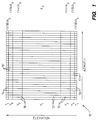
- a top view of a two-dimensional transducer array 10 is shown as including seven transducer elements in an elevational direction and thirty-two transducer elements in an azimuthal direction.
- the transducer elements 12 at elevation Y1 have the greatest transverse area, with elements 13 and 14 having the smallest transverse area.
- the comparative areas of elements 12, 13 and 14, as well as those of elements 15, 16, 17 and 18, are indicated in Fig. 1.
- Varying the transverse area of transducer elements 12-13 with elevation improves the acoustical properties of the two-dimensional array 10.
- the array may be focused electronically. While electronic focusing improves echographic procedures, the changes in electrical impedance across the elements will vary proportionally with the changes in transverse areas, so that driving the elements becomes more problematic. As will be explained more fully below, the effect of changes in area is at least partially offset in the present invention, thereby allowing conventional drive circuitry to be used for each of the transducer elements.
- the present invention varies "specific impedance," i.e. impedance per unit area, to normalize the electrical impedances of the transducer elements in the array.
- Figs. 2A and 2B illustrate alternative embodiments of a single transducer element of Fig. 1.
- Fig. 2A is a resonator stack of two piezoelectric layers 20A and 20B.
- the piezoelectric layers have equal thicknesses and are wired in an electrically parallel arrangement.
- the two layers have opposite poling vectors, as indicated by the vertically directed arrows.
- piezoelectric is defined as any material that generates mechanical waves in response to an electrical field applied across the material. Piezoelectric ceramics and polymers are known.
- the transducer element of Fig. 2A includes a pair of external electrodes 22A and 22D that are connected by a side electrode 23B. Internal electrodes 22B and 22C are linked by a side electrode 23A.
- Edge dielectric layers 21A, 21B, 21C and 21D physically separate electrodes 22A and 22D from electrodes 22B and 22C. Moreover, the edge dielectric layers minimize excitation of undesired lateral modes within the piezoelectric layers 22A and 22B. During the transmission of acoustic waves the lateral modes may arise from fringe electrical fields for previously poled piezoelectric material or from fringe fields for multilayer piezoelectric resonator stacks poled in situ. If electrodes were allowed to directly contact the opposed parallel sides of the piezoelectric layers, lateral modes could be excited within the piezoelectric layers. The type and properties of the material chosen for the edge dielectric layers determine the magnitudes of the fringe electric fields.
- the distance of separation between the electrode 22A and the side of electrode 22B, as provided by the edge dielectric layer 21A, preferably lies in the range of 10-250 mm. This separation must nominally stand off both the poling voltages and the operational applied voltages.
- Suitable dielectric materials for the edge dielectric layers, as well as internal dielectric layers 24A and 24B include: oxides, such as SiO z (Z ⁇ 1); ceramics, such as Al2O3 and PZT; refractory metals, such as Si x N y , BN and AlN; semiconductors, such as Si, Ge and GaAs; and polymers, such as epoxy and polyimide.
- oxides such as SiO z (Z ⁇ 1)
- ceramics such as Al2O3 and PZT
- refractory metals such as Si x N y , BN and AlN
- semiconductors such as Si, Ge and GaAs
- polymers such as epoxy and polyimide.
- a voltage signal source 29A is utilized to provide an excitation signal to the piezoelectric layers 20A and 20B.
- a differential amplifier 29B is employed, as well known in the art.
- Fig. 2A illustrates a situation in which the number of piezoelectric layers 20A and 20B is even and the external electrodes 22A and 22D have the same polarity.
- Fig. 2B illustrates an odd number of piezoelectric layers 20A, 20B and 20C, with external electrodes 22A and 22F having opposite polarity.
- Adjacent piezoelectric layers are attached using internal dielectric layers 24A and 24B, as well as bonding layers 25A, 25B, 25C and 25D.
- the thicknesses of the electrodes 22A-22D, the bonding layers 25A-25D and the internal dielectric layers 24A-24B are illustrated with exaggerated thicknesses for clarity. Typical thicknesses of the bonding layers and of the internal dielectric layers are less than 1 ⁇ m, and less than 100 ⁇ m, respectively.
- Electrodes 23A and 23B are optional, since the electrode layers 21A-21F can be electrically connected to one terminal of a group of one or more voltage sources 29A or differential amplifiers 29B. If the internal dielectric layers and the bonding layers are deleted, some of the intermediate electrode layers, such as 22B and 22C, can be optionally deleted.
- Fig. 3 illustrates an acoustic transducer element wired for fixed electrically parallel excitation, with alternating poling directions for three piezoelectric layers 30A, 30B and 30C.
- the transducer element includes the three piezoelectric layers, three pairs of edge dielectric layers 31A/31B, 31C/31D and 31E/31F, three pairs of individually controlled electrodes 32A/32B, 32C/32D and 32E/32F that surround the respective piezoelectric layers, and side electrodes 33A and 33B.
- the internal dielectric layers that separate the electrodes are not shown in Fig. 3.
- An optional backing layer may be included.
- the backing layer is made of a material which absorbs ultrasonic waves in order to eliminate reflections from the back side of the piezoelectric layer 30C.
- a front matching layer 36 for matching the acoustic impedance of the transducer element to the material to which acoustic waves 38 are to be transmitted may also be used.
- a suitable material for the backing layer may be a heavy metal, such as tungsten, in a lighter matrix such as a polymer or a ceramic.
- a suitable material for the front matching layer includes graphite, epoxy, polyimide or other similar compounds with an acoustic impedance between that of the piezoelectric material and the ambient medium.
- Fig. 4 illustrates a refinement of the electrical connection between first and second conductive electrodes 42A or 42B and an external or side electrode 43.
- the reliability of the electrical contact can be improved by providing rounded or arcuate surfaces 44A and 44B on the adjacent edge dielectric 41A and 41B and rounded or arcuate surfaces 45A and 45B at the interface of the two conductive electrodes 42A and 42B with the external electrode 43.
- the external electrode 43 is deposited over the piezoelectric layers 44A and 44B and the edge dielectrics 41A and 41B are bonded together, thereby allowing the external electrode to conform to the geometry of the rounded corners as shown.
- a multilayer piezoelectric resonator stack has several useful features, if the individual piezoelectric layers are of uniform thickness and the adjacent piezoelectric layers have opposite poling directions. In this configuration, the piezoelectric layers act mechanically in series, but act electrically in parallel.
- Fig. 5 illustrates how impedance reduction can be achieved for a multilayer transducer element if the piezoelectric layers are electrically connected in parallel.
- a single piezoelectric layer of thickness T (the "comparison layer") requires an applied voltage of B O
- a multilayer resonator stack of N piezoelectric layer, also of thickness T, constructed as illustrated in Figs. 2A and 2B with parallel electrical connections requires an applied voltage of only V0/N to achieve an equivalent piezoelectric stress field.. This occurs because of the reduced piezoelectric layer thickness between adjacent electrodes.
- the required applied transmit voltage for the comparison layer is 50-200 volts, the required applied voltage for a multilayer resonator stack can be reduced to the range of 5-15 volts, which is suitable for integration with high density integrated circuits.
- the electrical bandwidth of an N-layer resonator stack can also be increased relative to the bandwidth of the comparison layer.
- Each piezoelectric layer in the multilayer resonator stack is a lambda/2 resonator operating at N times the fundamental frequency F O for the comparison single resonator, neglecting the effect of strong coupling between piezoelectric layers.
- a multilayer resonator stack can also operate as a multifrequency acoustic transducer with a plurality of discrete fundamental frequencies.
- Figs. 6A and 6B illustrate how voltage reduction can be achieved for a multilayer transducer element where the piezoelectric layers are electrically connected in parallel, and how multifrequency operation can be achieved if the electrical connections of individual piezoelectric layers are programmable.
- an applied voltage of V O gives a resonance frequency of F O , for a thickness of lambda/2.
- the required applied voltage to achieve the independent total electric field in the three-layer resonator stack is V O /3.
- the possible resonance frequencies are F O , 3F O /2 and 3F O , using two, three or one piezoelectric sublayers in combination, respectively.
- Figs. 7A, 7B, 7C and 7D illustrate the effect on the spatial distribution of the electric field E and the fundamental resonant frequency of the piezoelectric resonator stack for parallel electrical connections for both parallel and opposite poling directions in adjacent piezoelectric layers. Positioned below each transducer configuration is a plot of the electric field as a function of distance x, measured from front to back (or inversely, through a multilayer piezoelectric stack).
- Fig. 7A has two piezoelectric layers 71A and 71B with opposite poling directions.
- Fig. 7B illustrates two piezoelectric layers 72A and 72B having parallel poling directions.
- FIG. 7A and 7B produce resonant frequencies of F O and 2F O , respectively.
- Fig. 7C illustrates three piezoelectric layers 73A, 73B and 73C having opposite poling directions for adjacent piezoelectric layers.
- Fig. 7D illustrates three piezoelectric layers 74A, 74B and 74C having parallel poling directions.
- Figs. 7C and 7D produce resonant frequencies of F O and 3F O , respectively.
- Fig. 8 illustrates an embodiment in which a transducer element is a right circular cylinder having three piezoelectric layers 80A, 80B and 80C.
- An acoustic wave 88 is shown for both the transmit and receive modes of operation.
- the three piezoelectric layers are shown without internal conductive electrodes and bonding layers for clarity.
- Two external electrodes 83A and 83B of opposite polarity are connected to the bottom and top of the transducer element and partially wrap around the sides of the piezoelectric layers.
- Insulating dielectric layers 85A and 85B isolate the two external electrodes.
- a voltage source 89A for the transmit mode and a differential amplifier 89B for the receive mode are also incorporated.
- Figs. 9A and 9B define an embodiment having three piezoelectric layers 90A, 90B and 90C that are individually addressable for multifrequency operation.
- the piezoelectric layers 90A, 90B and 90C have respective conductive electrode pairs 92A/92B, 92C/92D and 92E/92F, respective edge dielectric pairs 91A/91B, 91C/91D and 91E/91F, and bonding layers 95A, 95B, 95C and 95D.
- the internal electrodes 92B, 92C, 92D and 92E are isolated by internal dielectric layers 94A and 94B. Each of the electrodes is connected to an individual signal line 93A, 93B, 93C, 93D, 93E and 93F, respectively, all of which are connected to a multiplexer circuit 97.
- a voltage source 99A for the transmit mode and a differential amplifier 99B for the receive mode are also provided.
- the table shown in Fig. 9B exhibits the various voltage assignments required for the signal lines 93A-93F to produce resonant frequencies of F O , 3F O /2, and 3F O . For example, an assignment of voltage V O to signal lines 93B, 93C and 93F will produce a resonant frequency F O .
- a multifrequency transducer element may also be constructed by use of nonuniform thicknesses for the piezoelectric layers. These nonuniform piezoelectric layers may be assembled from uniform thickness layers that are permanently connected together to form nonuniform thickness layers.
- Figs. 10A-10F illustrate multifrequency operation from the largest nonredundant integer resonator stack, i.e. the largest resonator stack whose members have integer ratios of thickness and for which there are no redundant frequencies. This resonator stack can produce resonant frequencies of F O , 1.2F O , 1.5F O , 2F O , 3F O and 6F O .
- Fig. 10A produces a resonant frequency F O with piezoelectric layers 100A, 100B and 100C connected in series.
- Fig. 10B produces a resonant frequency 1.2F O using piezoelectric layers 102A and 102B connected in series, while layer 102C is left inactive.
- Fig. 10C produces a resonant frequency 1.5F O by connecting piezoelectric layers 104B and 104C in series.
- Fig. 10D produces a resonant frequency 2F O using only the largest piezoelectric layer 106B, leaving layers 106A and 106B inactivated.
- Fig. 10E produces a resonant frequency 3F O using only piezoelectric layer 108A.
- Fig. 10A produces a resonant frequency F O with piezoelectric layers 100A, 100B and 100C connected in series.
- Fig. 10B produces a resonant frequency 1.2F O using piezoelectric layers 102A and 102B
- two-dimensional transducer arrays 10 may be used in echographic examinations. Excitation signals which energize the individual transducer elements 12-18 may be shifted in phase to radiate ultrasonic energy at a focal point. Controlling the phase of the excitation signals applied to the elements allows variations in the focus or steering angle. Improved focusing is available by changing the transverse areas of the elements as shown in Fig. 1.
- a two-dimensional array has an infinite number of equal sized transducer elements that allow the array to act as a piecewise step approximation of a cylindrical lens.
- practical considerations significantly limit the number of transducer elements.
- the array of Fig. 1 utilizes transducer elements of different sizes to achieve improved acoustical characteristics.
- One difficulty with this approach is that a change in the transverse area of a transducer element 12-18 affects the electrical load presented to driving circuitry by the transducer element.
- the electrical impedance of an element is inversely proportional to the transverse area of the element. Consequently, the electrical impedance of each transducer element 12 is 1/9, i.e. 11%, the electrical impedance of each transducer element 17.
- Using the same driving circuitry for each of the transducer elements 12-18 would create significant impedance mismatches for at least some of the connections.
- the driving circuitry can be modified according to the number of different element areas, but the modification would add to the complexity and the expense of manufacturing an ultrasonic device.
- each piezoelectric layer of a particular multilayer transducer element 12-18 is connected to the remaining piezoelectric layers of that element in a manner to at least partially offset the effect of changes in transverse area. For example, if the elements each have three piezoelectric layers, the difference in transverse area between element 12 and element 17 can be completely offset by utilizing the layer connections of Figs. 11A and 11B. The series arrangement of Fig. 11A will induce an electrical impedance that is nine times greater than the parallel arrangement of Fig. 11B, all other factors being equal. Because the different wiring arrangements can be used to adjust the specific impedances of the transducer elements, substantially the same electrical load can be presented to driving circuitry by each transducer element despite the differences in transverse areas.
- the difference in transverse areas between elements 12 and elements 15 can be partially offset by utilizing the series-parallel wiring arrangement of 11C in connecting the three layers of transducer elements 15.
- the difference in areas would otherwise induce an electrical impedance at elements 15 that would be four times the impedance of elements 12, but the series-parallel arrangement adjusts the specific impedance so as to provide an electrical impedance that is approximately 22% of that established by a purely series electrical arrangement.
- An impedance equalization would be preferred, but is not critical. An arrangement closer to the ideal is possible by increasing the number of layers, but this would also increase the cost of fabrication.
- transducer element 15 may be made of a piezoelectric material having a higher dielectric constant than the material in forming elements 12, thereby at least partially offsetting the effect of the difference in areas.
- the embodiment of electrically arranging the piezoelectric layers of an element 12-18 is preferred to the embodiment of varying the piezoelectric materials, since different materials will have characteristics, e.g., coefficients of thermal expansion, that affect operation. Moreover, the choice of piezoelectric materials is limited. In any case, utilizing different piezoelectric materials adds to the complexity of fabrication. The additional complexity is particularly acute if greater impedance control is acquired by varying the piezoelectric material from layer to layer in a single transducer element 12-18.
- a third embodiment is to vary the thickness of the transducer elements 12-18 with changes in transverse area. Thickness is directly proportional to electrical impedance. However, in most applications, this embodiment is not practical, since changing the thickness of a transducer element will change the resonant frequency as well.
- the degrees of poling may be manipulated to provide impedance normalization.
- the impedance of poled material is higher at the resonant frequency.
- the electrical impedance can be varied as desired.
- electrically rewiring the transducer elements 12-18 is preferred, since varying degrees of poling will vary electrode-to-piezoelectric layer coupling. Poling strengthens the coupling for electrical-to-mechanical conversion, and vice versa. Consequently, in this embodiment a reduction in impedance is possible only by a loss of efficiency.
- the present invention may also be used with an annular array 130 in which the radiating regions of the transducer elements 132, 134, 136, 138 and 140 have concentric ring shapes.
- each ring has been given an equal area, so that the rings become thinner with the distance of a ring from the center. This arrangement does not maximize the focusing ability of the array.
- Employing the present invention with the annular two-dimensional array allows a designer to select transverse areas based upon operational considerations other than electrical impedance.
- the outer radii of the transducer elements 132-140 may be 4.5 mm, 5.3 mm, 6.0 mm, 6.7 mm and 7.5 mm, respectively.
- the electrical impedances of transducer elements 136 and 138 would be more than six times the electrical impedance of the largest transducer element 132.
- the electrical impedances can be normalized to improve the electrical performance of the array.
- the layers of transducer element 132 may be connected in electrical parallel, while the layers of transducer elements 136 and 138 may be connected in electrical series. The layers of the remaining transducer elements 134 and 140 would then be connected in a series-parallel arrangement to achieve an intermediate specific impedance for electrical-impedance normalization.
- the changes in electrical impedance as provided by the series, parallel and series-parallel arrangements of Figs. 11A-11D for different transducer elements in a two-dimensional array can also be utilized for arrays in which each element has a uniform size.
- the various layers are individually addressable by a switching mechanism such as the multiplexer 97 shown in Fig. 9A.
Abstract
A two-dimensional ultrasonic transducer array (10) includes a plurality of transducer elements (12-18), with each element having a plurality of piezoelectric layers (120A, 120B and 120C). The transducer elements vary in transverse areas of radiating regions. The effect of the variations in transverse areas on the electrical impedances of the elements is at least partially offset by varying the specific impedance, i.e., impedance per unit area, of the transducer elements in the array. In a preferred embodiment, the specific impedance is varied by selecting the electrical arrangements of piezoelectric layers in each element according to the transverse area of the element. Series, parallel and series-parallel arrangements are employed. This impedance normalization improves the electrical connection of the transducer elements to driving circuitry (29A). In alternative embodiments, impedance normalization is achieved by varying element thicknesses, element materials and/or degrees of poling across the two-dimensional array.
Description
- The present invention relates generally to acoustic transducers and more particularly to two-dimensional ultrasonic transducer arrays.
- A diagnostic ultrasonic imaging system for medical use forms images of tissues of a human body by electrically exciting a transducer element or an array of transducer elements to generate short ultrasonic pulses, which are caused to travel into the body. Echoes from the tissues are received by the transducer element or array of transducer elements and are converted into electrical signals. The electrical signals are amplified and used to form a cross sectional image of the tissues. Echographic examination is also used outside of the medical field.
- While a number of advances have been made in echographic examining, further advances in optimizing acoustical properties of a transducer face the potential problem of sacrificing desired electrical properties. Initially, an imaging transducer consisted of a single transducer element. Acoustical properties were improved by providing a transducer formed by a one-dimensional array of transducer elements. Conventionally, one-dimensional transducer arrays have a rectangular or circular configuration, but this is not critical. Acoustical properties may be improved by providing a two-dimensional array in either a rectangular or annular configuration.
- Focusing plays an important role in optimizing the acoustical properties of a transducer device. U.S. Pat. No. 4,477,783 to Glenn describes a mechanical lens used to focus acoustic energy to and from a single transducer element. Electronic focusing provides an alternative to the mechanical lens. Two-dimensional arrays can be phased by delaying signals to selected transducer elements so as to achieve a desired direction and focal range. Electronically focused transducer arrays offer the advantage that they can be held stationary during an echographic examination, potentially increasing resolution and the useful life of the device. The transducer elements are equal in size, so that a two-dimensional array can form a piecewise approximation of the desired curved delay profile. In order to reduce the total number of transducer elements, the number of transducer elements in the elevation dimension can be reduced. To obtain acceptable focusing properties, these elevation transducer elements are often different sizes to form a coarser piecewise linear approximation of the desired curved delay profile. The problem is that there are difficulties in employing the same driving circuitry to efficiently drive transducer elements of different sizes since the area of a radiating region of a transducer element is inversely proportional to the electrical impedance of that transducer element.
- It is an object of the present invention to provide a transducer device having a plurality of transducer elements that can be efficiently driven using conventional driving circuitry without regard for comparative sizes of the transducer elements.
- The above object has been met by a two-dimensional array of transducer elements with varying transverse areas, but with specific impedances that are adjusted inversely with transverse area. The specific impedances are selected to normalize electrical impedances across the array, so that driving circuitry can be efficiently coupled to each transducer element. Varying the transverse areas of the transducer elements in a two-dimensional array presents variations in the electrical load. "Impedance normalization" is defined as at least partially offsetting the effect of the differences in transverse areas. "Specific impedance" is defined as the impedance of a transducer element per unit area. Thus, unlike the electrical impedance to coupling to the driving circuitry, specific impedance is area-independent. The transducer device of the present invention utilizes a multilayer structure to maintain a generally constant ratio of electrical impedance to transverse area at each transducer element in the two-dimensional array.
- In a preferred embodiment, varying the specific impedances of transducer elements is achieved by electrically connecting piezoelectric layers of each multilayer transducer element such that the piezoelectric layers are in series, parallel or series-parallel arrangements. A series arrangement of piezoelectric layers induces a higher electrical impedance than would be induced by a parallel arrangement. Since electrical impedance of an element is inversely proportional to the transverse area of the element, the impedance of a first element having an area less than that of a second element can be normalized by connecting the piezoelectric layers of the first element in parallel and the piezoelectric layers of the second element in series. Impedance normalization of a third transducer element having an area greater than the first element but less than the second element can be achieved by providing a series-parallel electrical circuit of piezoelectric layers at the third transducer element.
- The two-dimensional array may have a large number of different sized transducer elements. Ideally, the differences in electrical circuits of piezoelectric layers completely offset the variations in size, so that the ratio of electrical impedance to transverse area is equal across the array. However, this ideal may not be achievable without increasing the number of piezoelectric layers beyond a practical limit. In such cases, the electrical circuits of piezoelectric layers should be connected to approach a norm, rather than to obtain an exact value of impedance at each element.
- In a second embodiment, impedance normalization is achieved by varying the thickness of the transducer elements in proportionally corresponding manner to variations in transverse area. However, changes in thickness affect the resonant frequency. In a third embodiment, the selected piezoelectric material varies with the transverse area of the elements. A piezoelectric layer having a higher dielectric constant will have a lower electrical impedance. Adjacent transducer elements may be made of different piezoelectric materials according to comparative transverse areas. Alternatively, different layers within a single transducer element may be comprised of different piezoelectric materials. A difficulty with this embodiment is that it adds complexity to the fabrication of the two-dimensional array. In a last embodiment, the degree of poling may be used to affect the specific impedance. A perfectly poled material will have a higher impedance at a resonant frequency. While degrees of poling may be used to control impedance, a relaxation of poling has the negative effect of reducing coupling efficiency, i.e. the efficiency of converting an electrical signal to mechanical waves and vice versa.
- The two-dimensional array may be rectangular or annular or may have any other configuration. The use of different electrical connection of piezoelectric layers within a single transducer element may be used to control impedances of adjacent transducer elements for purposes other than normalizing impedances of elements having different transverse areas. However, the main advantage of the present invention is that impedance normalization can be achieved so as to allow electronic focusing of the array without compromising the coupling of driving circuitry to the array. That is, the present invention eliminates the tradeoff between optimizing acoustical properties of the array and optimizing electrical properties.
- Fig. 1 illustrates one embodiment for achievement of impedance normalization for two-dimensional arrays based on impedance control in accordance with the present invention.
- Figs. 2A and 2B illustrate the difference between an even number of layers and an odd number of layers in a resonator stack.
- Fig. 3 illustrates the multilayer resonator stack assembled into a transducer.
- Fig. 4 illustrates use of a curvilinear interface of an edge dielectric layer and adjacent electrodes.
- Figs. 5A and 5B illustrate achievement of reduced impedance for multilayer transducers.
- Figs. 6A and 6B illustrate achievement of voltage reduction and multifrequency operation for multilayer transducers.
- Figs. 7A, 7B, 7C and 7D illustrate the effect of poling direction on two-layer and three-layer structures.
- Fig. 8 illustrates a cylindrical multilayer transducer structure.
- Figs. 9A and 9B illustrate multifrequency operation of a transducer using isolated internal electrode layer and a multiplexer circuit.
- Figs. 10A-10F illustrate multifrequency operation using the largest nonredundant integer resonator stack.
- Figs. 11A-11D illustrate achievement of impedance control based on series/parallel interconnection combinations.
- Fig. 12 is a top view of an annular array of transducer elements for achievement of impedance normalization based on impedance control in accordance with the present invention.
- With reference to Fig. 1, a top view of a two-
dimensional transducer array 10 is shown as including seven transducer elements in an elevational direction and thirty-two transducer elements in an azimuthal direction. Thetransducer elements 12 at elevation Y₁ have the greatest transverse area, withelements elements elements - Varying the transverse area of transducer elements 12-13 with elevation improves the acoustical properties of the two-
dimensional array 10. In a manner known in the art, the array may be focused electronically. While electronic focusing improves echographic procedures, the changes in electrical impedance across the elements will vary proportionally with the changes in transverse areas, so that driving the elements becomes more problematic. As will be explained more fully below, the effect of changes in area is at least partially offset in the present invention, thereby allowing conventional drive circuitry to be used for each of the transducer elements. The present invention varies "specific impedance," i.e. impedance per unit area, to normalize the electrical impedances of the transducer elements in the array. - Figs. 2A and 2B illustrate alternative embodiments of a single transducer element of Fig. 1. Fig. 2A is a resonator stack of two
piezoelectric layers - The transducer element of Fig. 2A includes a pair of
external electrodes side electrode 23B.Internal electrodes side electrode 23A. - Edge
dielectric layers separate electrodes electrodes piezoelectric layers electrode 22A and the side ofelectrode 22B, as provided by theedge dielectric layer 21A, preferably lies in the range of 10-250 mm. This separation must nominally stand off both the poling voltages and the operational applied voltages. Suitable dielectric materials for the edge dielectric layers, as well as internaldielectric layers 24A and 24B, include: oxides, such as SiOz (Z ≧ 1); ceramics, such as Al₂O₃ and PZT; refractory metals, such as SixNy, BN and AlN; semiconductors, such as Si, Ge and GaAs; and polymers, such as epoxy and polyimide. - In a transmit mode, a
voltage signal source 29A is utilized to provide an excitation signal to thepiezoelectric layers differential amplifier 29B is employed, as well known in the art. - Fig. 2A illustrates a situation in which the number of
piezoelectric layers external electrodes piezoelectric layers external electrodes dielectric layers 24A and 24B, as well as bonding layers 25A, 25B, 25C and 25D. The thicknesses of theelectrodes 22A-22D, the bonding layers 25A-25D and the internaldielectric layers 24A-24B are illustrated with exaggerated thicknesses for clarity. Typical thicknesses of the bonding layers and of the internal dielectric layers are less than 1 µm, and less than 100 µm, respectively. -
Side electrodes more voltage sources 29A ordifferential amplifiers 29B. If the internal dielectric layers and the bonding layers are deleted, some of the intermediate electrode layers, such as 22B and 22C, can be optionally deleted. - Fig. 3 illustrates an acoustic transducer element wired for fixed electrically parallel excitation, with alternating poling directions for three
piezoelectric layers dielectric layers 31A/31B, 31C/31D and 31E/31F, three pairs of individually controlledelectrodes 32A/32B, 32C/32D and 32E/32F that surround the respective piezoelectric layers, andside electrodes piezoelectric layer 30C. Afront matching layer 36, for matching the acoustic impedance of the transducer element to the material to whichacoustic waves 38 are to be transmitted may also be used. A suitable material for the backing layer may be a heavy metal, such as tungsten, in a lighter matrix such as a polymer or a ceramic. A suitable material for the front matching layer includes graphite, epoxy, polyimide or other similar compounds with an acoustic impedance between that of the piezoelectric material and the ambient medium. - Fig. 4 illustrates a refinement of the electrical connection between first and second
conductive electrodes side electrode 43. The reliability of the electrical contact can be improved by providing rounded orarcuate surfaces 44A and 44B on theadjacent edge dielectric arcuate surfaces conductive electrodes external electrode 43. Theexternal electrode 43 is deposited over thepiezoelectric layers 44A and 44B and theedge dielectrics - A multilayer piezoelectric resonator stack has several useful features, if the individual piezoelectric layers are of uniform thickness and the adjacent piezoelectric layers have opposite poling directions. In this configuration, the piezoelectric layers act mechanically in series, but act electrically in parallel. Fig. 5 illustrates how impedance reduction can be achieved for a multilayer transducer element if the piezoelectric layers are electrically connected in parallel. For a piezoelectric layer of capacitanc


- The electrical bandwidth of an N-layer resonator stack can also be increased relative to the bandwidth of the comparison layer. Each piezoelectric layer in the multilayer resonator stack is a lambda/2 resonator operating at N times the fundamental frequency FO for the comparison single resonator, neglecting the effect of strong coupling between piezoelectric layers. With an appropriate choice of series and parallel electrical connections to the individual electrodes between the piezoelectric layers, a multilayer resonator stack can also operate as a multifrequency acoustic transducer with a plurality of discrete fundamental frequencies.
- Figs. 6A and 6B illustrate how voltage reduction can be achieved for a multilayer transducer element where the piezoelectric layers are electrically connected in parallel, and how multifrequency operation can be achieved if the electrical connections of individual piezoelectric layers are programmable. For a single
piezoelectric layer 60, an applied voltage of VO gives a resonance frequency of FO, for a thickness of lambda/2. For a transducer element having threepiezoelectric layers - Figs. 7A, 7B, 7C and 7D illustrate the effect on the spatial distribution of the electric field E and the fundamental resonant frequency of the piezoelectric resonator stack for parallel electrical connections for both parallel and opposite poling directions in adjacent piezoelectric layers. Positioned below each transducer configuration is a plot of the electric field as a function of distance x, measured from front to back (or inversely, through a multilayer piezoelectric stack). Fig. 7A has two
piezoelectric layers piezoelectric layers piezoelectric layers piezoelectric layers - Fig. 8 illustrates an embodiment in which a transducer element is a right circular cylinder having three
piezoelectric layers acoustic wave 88 is shown for both the transmit and receive modes of operation. The three piezoelectric layers are shown without internal conductive electrodes and bonding layers for clarity. Twoexternal electrodes dielectric layers voltage source 89A for the transmit mode and adifferential amplifier 89B for the receive mode are also incorporated. - Multifrequency operation may be achieved if the electrodes are individually addressable. This requires use of thin electrical isolation layers that minimally perturb an acoustic wave that passes therethrough. Figs. 9A and 9B define an embodiment having three
piezoelectric layers piezoelectric layers dielectric pairs 91A/91B, 91C/91D and 91E/91F, andbonding layers internal electrodes dielectric layers 94A and 94B. Each of the electrodes is connected to anindividual signal line multiplexer circuit 97. Avoltage source 99A for the transmit mode and adifferential amplifier 99B for the receive mode are also provided. The table shown in Fig. 9B exhibits the various voltage assignments required for thesignal lines 93A-93F to produce resonant frequencies of FO, 3FO/2, and 3FO. For example, an assignment of voltage VO to signallines - A multifrequency transducer element may also be constructed by use of nonuniform thicknesses for the piezoelectric layers. These nonuniform piezoelectric layers may be assembled from uniform thickness layers that are permanently connected together to form nonuniform thickness layers. Figs. 10A-10F illustrate multifrequency operation from the largest nonredundant integer resonator stack, i.e. the largest resonator stack whose members have integer ratios of thickness and for which there are no redundant frequencies. This resonator stack can produce resonant frequencies of FO, 1.2FO, 1.5FO, 2FO, 3FO and 6FO.
- Fig. 10A produces a resonant frequency FO with
piezoelectric layers piezoelectric layers layer 102C is left inactive. Fig. 10C produces a resonant frequency 1.5FO by connectingpiezoelectric layers piezoelectric layer 106B, leavinglayers 106A and 106B inactivated. Fig. 10E produces a resonant frequency 3FO using only piezoelectric layer 108A. Fig. 10F produces a resonant frequency 6FO using only the thinnestpiezoelectric layer 110C. All resonator stacks having four or more piezoelectric layers with integer ratios of thicknesses generate a sequence of frequencies that include redundant frequencies. The ratio of individual layer thicknesses for a multilayer, multifrequency transducer element is not restricted to integral multiples of a single thickness. - As noted above with reference to Fig. 1, two-
dimensional transducer arrays 10 may be used in echographic examinations. Excitation signals which energize the individual transducer elements 12-18 may be shifted in phase to radiate ultrasonic energy at a focal point. Controlling the phase of the excitation signals applied to the elements allows variations in the focus or steering angle. Improved focusing is available by changing the transverse areas of the elements as shown in Fig. 1. Ideally, a two-dimensional array has an infinite number of equal sized transducer elements that allow the array to act as a piecewise step approximation of a cylindrical lens. However, practical considerations significantly limit the number of transducer elements. Thus, the array of Fig. 1 utilizes transducer elements of different sizes to achieve improved acoustical characteristics. - One difficulty with this approach is that a change in the transverse area of a transducer element 12-18 affects the electrical load presented to driving circuitry by the transducer element. The electrical impedance of an element is inversely proportional to the transverse area of the element. Consequently, the electrical impedance of each
transducer element 12 is 1/9, i.e. 11%, the electrical impedance of eachtransducer element 17. Using the same driving circuitry for each of the transducer elements 12-18 would create significant impedance mismatches for at least some of the connections. The driving circuitry can be modified according to the number of different element areas, but the modification would add to the complexity and the expense of manufacturing an ultrasonic device. - The present invention provides an impedance normalization for two-
dimensional transducer arrays 10. In a first embodiment, each piezoelectric layer of a particular multilayer transducer element 12-18 is connected to the remaining piezoelectric layers of that element in a manner to at least partially offset the effect of changes in transverse area. For example, if the elements each have three piezoelectric layers, the difference in transverse area betweenelement 12 andelement 17 can be completely offset by utilizing the layer connections of Figs. 11A and 11B. The series arrangement of Fig. 11A will induce an electrical impedance that is nine times greater than the parallel arrangement of Fig. 11B, all other factors being equal. Because the different wiring arrangements can be used to adjust the specific impedances of the transducer elements, substantially the same electrical load can be presented to driving circuitry by each transducer element despite the differences in transverse areas. - The difference in transverse areas between
elements 12 andelements 15 can be partially offset by utilizing the series-parallel wiring arrangement of 11C in connecting the three layers oftransducer elements 15. The difference in areas would otherwise induce an electrical impedance atelements 15 that would be four times the impedance ofelements 12, but the series-parallel arrangement adjusts the specific impedance so as to provide an electrical impedance that is approximately 22% of that established by a purely series electrical arrangement. An impedance equalization would be preferred, but is not critical. An arrangement closer to the ideal is possible by increasing the number of layers, but this would also increase the cost of fabrication. - Another embodiment of the present invention is to offset the differences in transverse areas by using different dielectric materials in forming the transducer elements. Electrical impedance is inversely proportional to the dielectric constant of the piezoelectric material. Consequently,
transducer element 15 may be made of a piezoelectric material having a higher dielectric constant than the material in formingelements 12, thereby at least partially offsetting the effect of the difference in areas. - The embodiment of electrically arranging the piezoelectric layers of an element 12-18 is preferred to the embodiment of varying the piezoelectric materials, since different materials will have characteristics, e.g., coefficients of thermal expansion, that affect operation. Moreover, the choice of piezoelectric materials is limited. In any case, utilizing different piezoelectric materials adds to the complexity of fabrication. The additional complexity is particularly acute if greater impedance control is acquired by varying the piezoelectric material from layer to layer in a single transducer element 12-18.
- A third embodiment is to vary the thickness of the transducer elements 12-18 with changes in transverse area. Thickness is directly proportional to electrical impedance. However, in most applications, this embodiment is not practical, since changing the thickness of a transducer element will change the resonant frequency as well.
- In yet another embodiment, the degrees of poling may be manipulated to provide impedance normalization. The impedance of poled material is higher at the resonant frequency. By providing degrees of poling, the electrical impedance can be varied as desired. Again, electrically rewiring the transducer elements 12-18 is preferred, since varying degrees of poling will vary electrode-to-piezoelectric layer coupling. Poling strengthens the coupling for electrical-to-mechanical conversion, and vice versa. Consequently, in this embodiment a reduction in impedance is possible only by a loss of efficiency.
- Referring now to Fig. 12, the present invention may also be used with an
annular array 130 in which the radiating regions of thetransducer elements - In Fig. 12, the outer radii of the transducer elements 132-140 may be 4.5 mm, 5.3 mm, 6.0 mm, 6.7 mm and 7.5 mm, respectively. In the absence of impedance normalization, the electrical impedances of
transducer elements largest transducer element 132. However, by fabricating each transducer element in the array to include a number of piezoelectric layers, and by adjusting the specific impedances of the different transducer elements in one of the manners described above, the electrical impedances can be normalized to improve the electrical performance of the array. For example, the layers oftransducer element 132 may be connected in electrical parallel, while the layers oftransducer elements transducer elements - The changes in electrical impedance as provided by the series, parallel and series-parallel arrangements of Figs. 11A-11D for different transducer elements in a two-dimensional array can also be utilized for arrays in which each element has a uniform size. Preferably, the various layers are individually addressable by a switching mechanism such as the
multiplexer 97 shown in Fig. 9A.
Claims (8)
- A transducer device comprising,
excitation means (29A) for supplying a signal to generate waves in piezoelectric material, and
an array (10) of piezoelectric transducer elements (12-18) electrically coupled to said excitation means, each transducer element having an impedance per unit area, said array including first and second transducer elements (12 and 13) having radiating regions having different transverse areas, said first and second transducer elements having differing impedances per unit area selected to normalize the electrical impedances of said first and second transducer elements to coupling to said excitation means. - The device of claim 1 wherein each transducer element (12-18) has a plurality of piezoelectric layers (120A, 120B and 120C), said first transducer element (12) having piezoelectric layers that are electrically connected in parallel and said second transducer element (13) having piezoelectric layers that are electrically connected in series to normalize the electrical impedances of said first and second transducer elements.
- The device of claim 1 wherein said first and second transducer elements (12 and 13) are elements in a two-dimensional array (10) of ultrasonic transducers.
- The device of claim 1 wherein each of said first and second transducer elements (12 and 13) includes electrode layers (122C and 122D) disposed between piezoelectric layers (120A, 120B and 120C).
- The device of claim 4 further comprising switching means (97) for varying interconnection of selected ones of said electrode layers (122C and 122D), thereby controlling the electrical impedances of said first and second transducer elements (12 and 13).
- The device of claim 1 wherein each transducer element (12-18) has a plurality of piezoelectric layers (120A, 120B and 120C), said transverse area of said first transducer element (12) being less than said transverse area of said second transducer element (13), piezoelectric layers of said first transducer element having a higher dielectric constant than piezoelectric layers of said second transducer element, thereby at least partially offsetting the effect of the difference in transverse areas with regard to electrical impedances of said first and second transducer elements.
- The device of claim 1 wherein said first and second transducer elements (12 and 13) are different with respect to at least one of thickness and degree of poling, thereby achieving said differing impedances per unit area.
- The device of claim 1 wherein said first and second radiating regions are annular regions (132 and 134) that are concentric.
Applications Claiming Priority (2)
| Application Number | Priority Date | Filing Date | Title |
|---|---|---|---|
| US29212 | 1993-03-10 | ||
| US08/029,212 US5381067A (en) | 1993-03-10 | 1993-03-10 | Electrical impedance normalization for an ultrasonic transducer array |
Publications (2)
| Publication Number | Publication Date |
|---|---|
| EP0615225A2 true EP0615225A2 (en) | 1994-09-14 |
| EP0615225A3 EP0615225A3 (en) | 1995-08-09 |
Family
ID=21847833
Family Applications (1)
| Application Number | Title | Priority Date | Filing Date |
|---|---|---|---|
| EP94300522A Withdrawn EP0615225A3 (en) | 1993-03-10 | 1994-01-25 | Electrical impedance normalization for an ultrasonic transducer array. |
Country Status (2)
| Country | Link |
|---|---|
| US (1) | US5381067A (en) |
| EP (1) | EP0615225A3 (en) |
Cited By (2)
| Publication number | Priority date | Publication date | Assignee | Title |
|---|---|---|---|---|
| WO2007149680A2 (en) * | 2006-06-22 | 2007-12-27 | Gooch And Housego Plc | Acoustic transducers having localized ferroelectric domain inverted regions |
| EP3653148A3 (en) * | 2009-06-24 | 2020-08-26 | Ethicon LLC | Ultrasonic surgical instruments |
Families Citing this family (217)
| Publication number | Priority date | Publication date | Assignee | Title |
|---|---|---|---|---|
| US6225728B1 (en) * | 1994-08-18 | 2001-05-01 | Agilent Technologies, Inc. | Composite piezoelectric transducer arrays with improved acoustical and electrical impedance |
| DE69416129T2 (en) * | 1994-10-10 | 1999-07-01 | Endress Hauser Gmbh Co | A method for operating an ultrasonic transducer and circuit arrangement for performing the method |
| US5629578A (en) * | 1995-03-20 | 1997-05-13 | Martin Marietta Corp. | Integrated composite acoustic transducer array |
| DE69736549T2 (en) * | 1996-02-29 | 2007-08-23 | Acuson Corp., Mountain View | SYSTEM, METHOD AND CONVERTER FOR ORIENTING MULTIPLE ULTRASOUND IMAGES |
| US5825117A (en) * | 1996-03-26 | 1998-10-20 | Hewlett-Packard Company | Second harmonic imaging transducers |
| US6016024A (en) * | 1996-04-05 | 2000-01-18 | Murata Manufacturing Co., Ltd. | Piezoelectric component |
| JP3266031B2 (en) * | 1996-04-18 | 2002-03-18 | 株式会社村田製作所 | Piezoelectric resonator and electronic component using the same |
| JP3271517B2 (en) * | 1996-04-05 | 2002-04-02 | 株式会社村田製作所 | Piezoelectric resonator and electronic component using the same |
| US5939819A (en) * | 1996-04-18 | 1999-08-17 | Murata Manufacturing Co., Ltd. | Electronic component and ladder filter |
| US5957851A (en) * | 1996-06-10 | 1999-09-28 | Acuson Corporation | Extended bandwidth ultrasonic transducer |
| JPH1079639A (en) * | 1996-07-10 | 1998-03-24 | Murata Mfg Co Ltd | Piezoelectric resonator and electronic component using the resonator |
| JPH1084244A (en) * | 1996-07-18 | 1998-03-31 | Murata Mfg Co Ltd | Piezoelectric resonator and electronic component using it |
| JP3271541B2 (en) * | 1996-07-26 | 2002-04-02 | 株式会社村田製作所 | Piezoelectric resonator and electronic component using the same |
| JP3577170B2 (en) * | 1996-08-05 | 2004-10-13 | 株式会社村田製作所 | Piezoelectric resonator, method of manufacturing the same, and electronic component using the same |
| JPH10107579A (en) * | 1996-08-06 | 1998-04-24 | Murata Mfg Co Ltd | Piezoelectric component |
| JPH10126203A (en) * | 1996-08-27 | 1998-05-15 | Murata Mfg Co Ltd | Piezoelectric resonator and electronic component using it |
| JP3267171B2 (en) * | 1996-09-12 | 2002-03-18 | 株式会社村田製作所 | Piezoelectric resonator and electronic component using the same |
| JPH10126202A (en) * | 1996-10-23 | 1998-05-15 | Murata Mfg Co Ltd | Piezoelectric resonator and electronic component using it |
| JP3147793B2 (en) * | 1996-11-22 | 2001-03-19 | 株式会社村田製作所 | Ladder type filter |
| JP3271538B2 (en) * | 1996-11-28 | 2002-04-02 | 株式会社村田製作所 | Piezoelectric resonator and electronic component using the same |
| US6045508A (en) * | 1997-02-27 | 2000-04-04 | Acuson Corporation | Ultrasonic probe, system and method for two-dimensional imaging or three-dimensional reconstruction |
| US5945770A (en) * | 1997-08-20 | 1999-08-31 | Acuson Corporation | Multilayer ultrasound transducer and the method of manufacture thereof |
| US6140740A (en) * | 1997-12-30 | 2000-10-31 | Remon Medical Technologies, Ltd. | Piezoelectric transducer |
| US20030036746A1 (en) * | 2001-08-16 | 2003-02-20 | Avi Penner | Devices for intrabody delivery of molecules and systems and methods utilizing same |
| US6416478B1 (en) | 1998-05-05 | 2002-07-09 | Acuson Corporation | Extended bandwidth ultrasonic transducer and method |
| US7024248B2 (en) | 2000-10-16 | 2006-04-04 | Remon Medical Technologies Ltd | Systems and methods for communicating with implantable devices |
| US7283874B2 (en) | 2000-10-16 | 2007-10-16 | Remon Medical Technologies Ltd. | Acoustically powered implantable stimulating device |
| US6764446B2 (en) | 2000-10-16 | 2004-07-20 | Remon Medical Technologies Ltd | Implantable pressure sensors and methods for making and using them |
| US6822374B1 (en) * | 2000-11-15 | 2004-11-23 | General Electric Company | Multilayer piezoelectric structure with uniform electric field |
| US7344501B1 (en) * | 2001-02-28 | 2008-03-18 | Siemens Medical Solutions Usa, Inc. | Multi-layered transducer array and method for bonding and isolating |
| US11229472B2 (en) | 2001-06-12 | 2022-01-25 | Cilag Gmbh International | Modular battery powered handheld surgical instrument with multiple magnetic position sensors |
| US6589180B2 (en) * | 2001-06-20 | 2003-07-08 | Bae Systems Information And Electronic Systems Integration, Inc | Acoustical array with multilayer substrate integrated circuits |
| US20030173870A1 (en) * | 2002-03-12 | 2003-09-18 | Shuh-Yueh Simon Hsu | Piezoelectric ultrasound transducer assembly having internal electrodes for bandwidth enhancement and mode suppression |
| US8182501B2 (en) | 2004-02-27 | 2012-05-22 | Ethicon Endo-Surgery, Inc. | Ultrasonic surgical shears and method for sealing a blood vessel using same |
| JP5009159B2 (en) | 2004-10-08 | 2012-08-22 | エシコン・エンド−サージェリィ・インコーポレイテッド | Ultrasonic surgical instrument |
| CA2589268A1 (en) * | 2004-11-24 | 2006-06-01 | Abraham Penner | Implantable medical device with integrated acoustic transducer |
| US7522962B1 (en) | 2004-12-03 | 2009-04-21 | Remon Medical Technologies, Ltd | Implantable medical device with integrated acoustic transducer |
| US7615012B2 (en) * | 2005-08-26 | 2009-11-10 | Cardiac Pacemakers, Inc. | Broadband acoustic sensor for an implantable medical device |
| US7570998B2 (en) * | 2005-08-26 | 2009-08-04 | Cardiac Pacemakers, Inc. | Acoustic communication transducer in implantable medical device header |
| US20070191713A1 (en) | 2005-10-14 | 2007-08-16 | Eichmann Stephen E | Ultrasonic device for cutting and coagulating |
| US9387515B2 (en) * | 2005-11-15 | 2016-07-12 | The Brigham And Women's Hospital, Inc. | Impedance matching for ultrasound phased array elements |
| US8078278B2 (en) * | 2006-01-10 | 2011-12-13 | Remon Medical Technologies Ltd. | Body attachable unit in wireless communication with implantable devices |
| US7621930B2 (en) | 2006-01-20 | 2009-11-24 | Ethicon Endo-Surgery, Inc. | Ultrasound medical instrument having a medical ultrasonic blade |
| US7650185B2 (en) * | 2006-04-25 | 2010-01-19 | Cardiac Pacemakers, Inc. | System and method for walking an implantable medical device from a sleep state |
| JP4839136B2 (en) * | 2006-06-02 | 2011-12-21 | 富士フイルム株式会社 | Ultrasonic transducer array, ultrasonic probe, ultrasonic endoscope, ultrasonic diagnostic equipment |
| WO2007145073A1 (en) * | 2006-06-13 | 2007-12-21 | Konica Minolta Medical & Graphic, Inc. | Array ultrasonic probe and its manufacturing method and array ultrasonic probe drive method |
| JP4897370B2 (en) * | 2006-06-28 | 2012-03-14 | 富士フイルム株式会社 | Ultrasonic transducer array, ultrasonic probe, ultrasonic endoscope, ultrasonic diagnostic equipment |
| US20080021328A1 (en) * | 2006-07-20 | 2008-01-24 | Konica Minolta Medical & Graphic, Inc. | Ultrasound probe and method of manufacturing ultrasound probe |
| WO2008011577A2 (en) | 2006-07-21 | 2008-01-24 | Cardiac Pacemakers, Inc. | Ultrasonic transducer for a metallic cavity implanted medical device |
| US7912548B2 (en) * | 2006-07-21 | 2011-03-22 | Cardiac Pacemakers, Inc. | Resonant structures for implantable devices |
| JP2008086362A (en) * | 2006-09-29 | 2008-04-17 | Fujifilm Corp | Ultrasonic probe, ultrasonic endoscope and ultrasonic diagnostic equipment |
| JP2008188415A (en) * | 2007-01-09 | 2008-08-21 | Konica Minolta Medical & Graphic Inc | Piezoelectric element, manufacturing method for it, and ultrasonic probe equipped with the piezoelectric element |
| US20080171941A1 (en) * | 2007-01-12 | 2008-07-17 | Huelskamp Paul J | Low power methods for pressure waveform signal sampling using implantable medical devices |
| US8057498B2 (en) | 2007-11-30 | 2011-11-15 | Ethicon Endo-Surgery, Inc. | Ultrasonic surgical instrument blades |
| US8142461B2 (en) | 2007-03-22 | 2012-03-27 | Ethicon Endo-Surgery, Inc. | Surgical instruments |
| US20080234709A1 (en) | 2007-03-22 | 2008-09-25 | Houser Kevin L | Ultrasonic surgical instrument and cartilage and bone shaping blades therefor |
| US8226675B2 (en) * | 2007-03-22 | 2012-07-24 | Ethicon Endo-Surgery, Inc. | Surgical instruments |
| US8911460B2 (en) | 2007-03-22 | 2014-12-16 | Ethicon Endo-Surgery, Inc. | Ultrasonic surgical instruments |
| JP5231525B2 (en) * | 2007-03-26 | 2013-07-10 | レモン メディカル テクノロジーズ, リミテッド | Biased acoustic switch for implantable medical devices |
| US8825161B1 (en) | 2007-05-17 | 2014-09-02 | Cardiac Pacemakers, Inc. | Acoustic transducer for an implantable medical device |
| EP2162185B1 (en) * | 2007-06-14 | 2015-07-01 | Cardiac Pacemakers, Inc. | Multi-element acoustic recharging system |
| US8348967B2 (en) * | 2007-07-27 | 2013-01-08 | Ethicon Endo-Surgery, Inc. | Ultrasonic surgical instruments |
| US8808319B2 (en) | 2007-07-27 | 2014-08-19 | Ethicon Endo-Surgery, Inc. | Surgical instruments |
| US8523889B2 (en) | 2007-07-27 | 2013-09-03 | Ethicon Endo-Surgery, Inc. | Ultrasonic end effectors with increased active length |
| US8882791B2 (en) | 2007-07-27 | 2014-11-11 | Ethicon Endo-Surgery, Inc. | Ultrasonic surgical instruments |
| US9044261B2 (en) * | 2007-07-31 | 2015-06-02 | Ethicon Endo-Surgery, Inc. | Temperature controlled ultrasonic surgical instruments |
| US8430898B2 (en) | 2007-07-31 | 2013-04-30 | Ethicon Endo-Surgery, Inc. | Ultrasonic surgical instruments |
| US8512365B2 (en) | 2007-07-31 | 2013-08-20 | Ethicon Endo-Surgery, Inc. | Surgical instruments |
| US8252012B2 (en) | 2007-07-31 | 2012-08-28 | Ethicon Endo-Surgery, Inc. | Ultrasonic surgical instrument with modulator |
| US8623027B2 (en) | 2007-10-05 | 2014-01-07 | Ethicon Endo-Surgery, Inc. | Ergonomic surgical instruments |
| US7901423B2 (en) | 2007-11-30 | 2011-03-08 | Ethicon Endo-Surgery, Inc. | Folded ultrasonic end effectors with increased active length |
| US10010339B2 (en) | 2007-11-30 | 2018-07-03 | Ethicon Llc | Ultrasonic surgical blades |
| US20090312650A1 (en) * | 2008-06-12 | 2009-12-17 | Cardiac Pacemakers, Inc. | Implantable pressure sensor with automatic measurement and storage capabilities |
| US8798761B2 (en) * | 2008-06-27 | 2014-08-05 | Cardiac Pacemakers, Inc. | Systems and methods of monitoring the acoustic coupling of medical devices |
| US20100004536A1 (en) * | 2008-07-03 | 2010-01-07 | Avner Rosenberg | Method and apparatus for ultrasound tissue treatment |
| US20100017750A1 (en) * | 2008-07-16 | 2010-01-21 | Avner Rosenberg | User interface |
| US20100023091A1 (en) * | 2008-07-24 | 2010-01-28 | Stahmann Jeffrey E | Acoustic communication of implantable device status |
| US8058771B2 (en) | 2008-08-06 | 2011-11-15 | Ethicon Endo-Surgery, Inc. | Ultrasonic device for cutting and coagulating with stepped output |
| US9089360B2 (en) * | 2008-08-06 | 2015-07-28 | Ethicon Endo-Surgery, Inc. | Devices and techniques for cutting and coagulating tissue |
| EP2361115A1 (en) * | 2008-10-27 | 2011-08-31 | Cardiac Pacemakers, Inc. | Methods and systems for recharging implantable devices |
| WO2010073920A1 (en) * | 2008-12-25 | 2010-07-01 | コニカミノルタエムジー株式会社 | Ultrasonic probe and method for fabricating ultrasonic probe |
| US20100298743A1 (en) * | 2009-05-20 | 2010-11-25 | Ethicon Endo-Surgery, Inc. | Thermally-activated coupling arrangements and methods for attaching tools to ultrasonic surgical instruments |
| US9700339B2 (en) * | 2009-05-20 | 2017-07-11 | Ethicon Endo-Surgery, Inc. | Coupling arrangements and methods for attaching tools to ultrasonic surgical instruments |
| KR101049736B1 (en) * | 2009-06-04 | 2011-07-19 | 전자부품연구원 | Array structure of pyroelectric infrared sensor and its manufacturing method |
| US8461744B2 (en) * | 2009-07-15 | 2013-06-11 | Ethicon Endo-Surgery, Inc. | Rotating transducer mount for ultrasonic surgical instruments |
| US9017326B2 (en) | 2009-07-15 | 2015-04-28 | Ethicon Endo-Surgery, Inc. | Impedance monitoring apparatus, system, and method for ultrasonic surgical instruments |
| US8663220B2 (en) * | 2009-07-15 | 2014-03-04 | Ethicon Endo-Surgery, Inc. | Ultrasonic surgical instruments |
| US11090104B2 (en) | 2009-10-09 | 2021-08-17 | Cilag Gmbh International | Surgical generator for ultrasonic and electrosurgical devices |
| US10441345B2 (en) | 2009-10-09 | 2019-10-15 | Ethicon Llc | Surgical generator for ultrasonic and electrosurgical devices |
| US8986302B2 (en) | 2009-10-09 | 2015-03-24 | Ethicon Endo-Surgery, Inc. | Surgical generator for ultrasonic and electrosurgical devices |
| USRE47996E1 (en) | 2009-10-09 | 2020-05-19 | Ethicon Llc | Surgical generator for ultrasonic and electrosurgical devices |
| US10172669B2 (en) | 2009-10-09 | 2019-01-08 | Ethicon Llc | Surgical instrument comprising an energy trigger lockout |
| US9168054B2 (en) | 2009-10-09 | 2015-10-27 | Ethicon Endo-Surgery, Inc. | Surgical generator for ultrasonic and electrosurgical devices |
| MX2012004815A (en) * | 2009-10-24 | 2012-06-25 | Syneron Medical Ltd | Method and apparatus for real time monitoring of tissue layers. |
| US8531064B2 (en) * | 2010-02-11 | 2013-09-10 | Ethicon Endo-Surgery, Inc. | Ultrasonically powered surgical instruments with rotating cutting implement |
| US8469981B2 (en) | 2010-02-11 | 2013-06-25 | Ethicon Endo-Surgery, Inc. | Rotatable cutting implement arrangements for ultrasonic surgical instruments |
| US8382782B2 (en) * | 2010-02-11 | 2013-02-26 | Ethicon Endo-Surgery, Inc. | Ultrasonic surgical instruments with partially rotating blade and fixed pad arrangement |
| US8486096B2 (en) * | 2010-02-11 | 2013-07-16 | Ethicon Endo-Surgery, Inc. | Dual purpose surgical instrument for cutting and coagulating tissue |
| US8323302B2 (en) * | 2010-02-11 | 2012-12-04 | Ethicon Endo-Surgery, Inc. | Methods of using ultrasonically powered surgical instruments with rotatable cutting implements |
| US8951272B2 (en) | 2010-02-11 | 2015-02-10 | Ethicon Endo-Surgery, Inc. | Seal arrangements for ultrasonically powered surgical instruments |
| US8579928B2 (en) | 2010-02-11 | 2013-11-12 | Ethicon Endo-Surgery, Inc. | Outer sheath and blade arrangements for ultrasonic surgical instruments |
| US9259234B2 (en) | 2010-02-11 | 2016-02-16 | Ethicon Endo-Surgery, Llc | Ultrasonic surgical instruments with rotatable blade and hollow sheath arrangements |
| US8419759B2 (en) * | 2010-02-11 | 2013-04-16 | Ethicon Endo-Surgery, Inc. | Ultrasonic surgical instrument with comb-like tissue trimming device |
| US8961547B2 (en) | 2010-02-11 | 2015-02-24 | Ethicon Endo-Surgery, Inc. | Ultrasonic surgical instruments with moving cutting implement |
| GB2480498A (en) | 2010-05-21 | 2011-11-23 | Ethicon Endo Surgery Inc | Medical device comprising RF circuitry |
| US8795327B2 (en) | 2010-07-22 | 2014-08-05 | Ethicon Endo-Surgery, Inc. | Electrosurgical instrument with separate closure and cutting members |
| US9192431B2 (en) | 2010-07-23 | 2015-11-24 | Ethicon Endo-Surgery, Inc. | Electrosurgical cutting and sealing instrument |
| US8968293B2 (en) | 2011-04-12 | 2015-03-03 | Covidien Lp | Systems and methods for calibrating power measurements in an electrosurgical generator |
| US9259265B2 (en) | 2011-07-22 | 2016-02-16 | Ethicon Endo-Surgery, Llc | Surgical instruments for tensioning tissue |
| USD700967S1 (en) | 2011-08-23 | 2014-03-11 | Covidien Ag | Handle for portable surgical device |
| WO2013043906A1 (en) | 2011-09-20 | 2013-03-28 | Sunnybrook Health Sciences Centre | Ultrasound transducer and method for making the same |
| JP5644729B2 (en) * | 2011-09-30 | 2014-12-24 | コニカミノルタ株式会社 | Ultrasonic transducer, ultrasonic probe, and ultrasonic diagnostic imaging apparatus |
| USD687549S1 (en) | 2011-10-24 | 2013-08-06 | Ethicon Endo-Surgery, Inc. | Surgical instrument |
| US9314292B2 (en) | 2011-10-24 | 2016-04-19 | Ethicon Endo-Surgery, Llc | Trigger lockout mechanism |
| EP2811932B1 (en) | 2012-02-10 | 2019-06-26 | Ethicon LLC | Robotically controlled surgical instrument |
| US9241731B2 (en) | 2012-04-09 | 2016-01-26 | Ethicon Endo-Surgery, Inc. | Rotatable electrical connection for ultrasonic surgical instruments |
| US9226766B2 (en) | 2012-04-09 | 2016-01-05 | Ethicon Endo-Surgery, Inc. | Serial communication protocol for medical device |
| US9237921B2 (en) | 2012-04-09 | 2016-01-19 | Ethicon Endo-Surgery, Inc. | Devices and techniques for cutting and coagulating tissue |
| US9439668B2 (en) | 2012-04-09 | 2016-09-13 | Ethicon Endo-Surgery, Llc | Switch arrangements for ultrasonic surgical instruments |
| US9724118B2 (en) | 2012-04-09 | 2017-08-08 | Ethicon Endo-Surgery, Llc | Techniques for cutting and coagulating tissue for ultrasonic surgical instruments |
| US20140005705A1 (en) | 2012-06-29 | 2014-01-02 | Ethicon Endo-Surgery, Inc. | Surgical instruments with articulating shafts |
| US9408622B2 (en) | 2012-06-29 | 2016-08-09 | Ethicon Endo-Surgery, Llc | Surgical instruments with articulating shafts |
| US9283045B2 (en) | 2012-06-29 | 2016-03-15 | Ethicon Endo-Surgery, Llc | Surgical instruments with fluid management system |
| US9326788B2 (en) | 2012-06-29 | 2016-05-03 | Ethicon Endo-Surgery, Llc | Lockout mechanism for use with robotic electrosurgical device |
| US9820768B2 (en) | 2012-06-29 | 2017-11-21 | Ethicon Llc | Ultrasonic surgical instruments with control mechanisms |
| US20140005702A1 (en) | 2012-06-29 | 2014-01-02 | Ethicon Endo-Surgery, Inc. | Ultrasonic surgical instruments with distally positioned transducers |
| US9351754B2 (en) | 2012-06-29 | 2016-05-31 | Ethicon Endo-Surgery, Llc | Ultrasonic surgical instruments with distally positioned jaw assemblies |
| US9393037B2 (en) | 2012-06-29 | 2016-07-19 | Ethicon Endo-Surgery, Llc | Surgical instruments with articulating shafts |
| US9198714B2 (en) | 2012-06-29 | 2015-12-01 | Ethicon Endo-Surgery, Inc. | Haptic feedback devices for surgical robot |
| US9226767B2 (en) | 2012-06-29 | 2016-01-05 | Ethicon Endo-Surgery, Inc. | Closed feedback control for electrosurgical device |
| BR112015007010B1 (en) | 2012-09-28 | 2022-05-31 | Ethicon Endo-Surgery, Inc | end actuator |
| US9095367B2 (en) | 2012-10-22 | 2015-08-04 | Ethicon Endo-Surgery, Inc. | Flexible harmonic waveguides/blades for surgical instruments |
| US10201365B2 (en) | 2012-10-22 | 2019-02-12 | Ethicon Llc | Surgeon feedback sensing and display methods |
| US20140135804A1 (en) | 2012-11-15 | 2014-05-15 | Ethicon Endo-Surgery, Inc. | Ultrasonic and electrosurgical devices |
| US10226273B2 (en) | 2013-03-14 | 2019-03-12 | Ethicon Llc | Mechanical fasteners for use with surgical energy devices |
| US9196817B2 (en) * | 2013-03-15 | 2015-11-24 | Lawrence Livermore National Security, Llc | High voltage switches having one or more floating conductor layers |
| US9241728B2 (en) | 2013-03-15 | 2016-01-26 | Ethicon Endo-Surgery, Inc. | Surgical instrument with multiple clamping mechanisms |
| US9814514B2 (en) | 2013-09-13 | 2017-11-14 | Ethicon Llc | Electrosurgical (RF) medical instruments for cutting and coagulating tissue |
| US9265926B2 (en) | 2013-11-08 | 2016-02-23 | Ethicon Endo-Surgery, Llc | Electrosurgical devices |
| GB2521229A (en) | 2013-12-16 | 2015-06-17 | Ethicon Endo Surgery Inc | Medical device |
| GB2521228A (en) | 2013-12-16 | 2015-06-17 | Ethicon Endo Surgery Inc | Medical device |
| US9795436B2 (en) | 2014-01-07 | 2017-10-24 | Ethicon Llc | Harvesting energy from a surgical generator |
| US9554854B2 (en) | 2014-03-18 | 2017-01-31 | Ethicon Endo-Surgery, Llc | Detecting short circuits in electrosurgical medical devices |
| US10463421B2 (en) | 2014-03-27 | 2019-11-05 | Ethicon Llc | Two stage trigger, clamp and cut bipolar vessel sealer |
| US10092310B2 (en) | 2014-03-27 | 2018-10-09 | Ethicon Llc | Electrosurgical devices |
| US9737355B2 (en) | 2014-03-31 | 2017-08-22 | Ethicon Llc | Controlling impedance rise in electrosurgical medical devices |
| US9913680B2 (en) | 2014-04-15 | 2018-03-13 | Ethicon Llc | Software algorithms for electrosurgical instruments |
| US10285724B2 (en) | 2014-07-31 | 2019-05-14 | Ethicon Llc | Actuation mechanisms and load adjustment assemblies for surgical instruments |
| US10639092B2 (en) | 2014-12-08 | 2020-05-05 | Ethicon Llc | Electrode configurations for surgical instruments |
| US10159524B2 (en) | 2014-12-22 | 2018-12-25 | Ethicon Llc | High power battery powered RF amplifier topology |
| US10245095B2 (en) | 2015-02-06 | 2019-04-02 | Ethicon Llc | Electrosurgical instrument with rotation and articulation mechanisms |
| US10321950B2 (en) | 2015-03-17 | 2019-06-18 | Ethicon Llc | Managing tissue treatment |
| US10342602B2 (en) | 2015-03-17 | 2019-07-09 | Ethicon Llc | Managing tissue treatment |
| US10595929B2 (en) | 2015-03-24 | 2020-03-24 | Ethicon Llc | Surgical instruments with firing system overload protection mechanisms |
| US10314638B2 (en) | 2015-04-07 | 2019-06-11 | Ethicon Llc | Articulating radio frequency (RF) tissue seal with articulating state sensing |
| US10034684B2 (en) | 2015-06-15 | 2018-07-31 | Ethicon Llc | Apparatus and method for dissecting and coagulating tissue |
| US11020140B2 (en) | 2015-06-17 | 2021-06-01 | Cilag Gmbh International | Ultrasonic surgical blade for use with ultrasonic surgical instruments |
| US10034704B2 (en) | 2015-06-30 | 2018-07-31 | Ethicon Llc | Surgical instrument with user adaptable algorithms |
| US10357303B2 (en) | 2015-06-30 | 2019-07-23 | Ethicon Llc | Translatable outer tube for sealing using shielded lap chole dissector |
| US11051873B2 (en) | 2015-06-30 | 2021-07-06 | Cilag Gmbh International | Surgical system with user adaptable techniques employing multiple energy modalities based on tissue parameters |
| US10898256B2 (en) | 2015-06-30 | 2021-01-26 | Ethicon Llc | Surgical system with user adaptable techniques based on tissue impedance |
| US11141213B2 (en) | 2015-06-30 | 2021-10-12 | Cilag Gmbh International | Surgical instrument with user adaptable techniques |
| US11129669B2 (en) | 2015-06-30 | 2021-09-28 | Cilag Gmbh International | Surgical system with user adaptable techniques based on tissue type |
| US10154852B2 (en) | 2015-07-01 | 2018-12-18 | Ethicon Llc | Ultrasonic surgical blade with improved cutting and coagulation features |
| US11033322B2 (en) | 2015-09-30 | 2021-06-15 | Ethicon Llc | Circuit topologies for combined generator |
| US10959771B2 (en) | 2015-10-16 | 2021-03-30 | Ethicon Llc | Suction and irrigation sealing grasper |
| US10595930B2 (en) | 2015-10-16 | 2020-03-24 | Ethicon Llc | Electrode wiping surgical device |
| US10959806B2 (en) | 2015-12-30 | 2021-03-30 | Ethicon Llc | Energized medical device with reusable handle |
| US10179022B2 (en) | 2015-12-30 | 2019-01-15 | Ethicon Llc | Jaw position impedance limiter for electrosurgical instrument |
| US10575892B2 (en) | 2015-12-31 | 2020-03-03 | Ethicon Llc | Adapter for electrical surgical instruments |
| US11229471B2 (en) | 2016-01-15 | 2022-01-25 | Cilag Gmbh International | Modular battery powered handheld surgical instrument with selective application of energy based on tissue characterization |
| US11129670B2 (en) | 2016-01-15 | 2021-09-28 | Cilag Gmbh International | Modular battery powered handheld surgical instrument with selective application of energy based on button displacement, intensity, or local tissue characterization |
| US11051840B2 (en) | 2016-01-15 | 2021-07-06 | Ethicon Llc | Modular battery powered handheld surgical instrument with reusable asymmetric handle housing |
| US10716615B2 (en) | 2016-01-15 | 2020-07-21 | Ethicon Llc | Modular battery powered handheld surgical instrument with curved end effectors having asymmetric engagement between jaw and blade |
| US10555769B2 (en) | 2016-02-22 | 2020-02-11 | Ethicon Llc | Flexible circuits for electrosurgical instrument |
| US10987156B2 (en) | 2016-04-29 | 2021-04-27 | Ethicon Llc | Electrosurgical instrument with electrically conductive gap setting member and electrically insulative tissue engaging members |
| US10646269B2 (en) | 2016-04-29 | 2020-05-12 | Ethicon Llc | Non-linear jaw gap for electrosurgical instruments |
| US10702329B2 (en) | 2016-04-29 | 2020-07-07 | Ethicon Llc | Jaw structure with distal post for electrosurgical instruments |
| US10485607B2 (en) | 2016-04-29 | 2019-11-26 | Ethicon Llc | Jaw structure with distal closure for electrosurgical instruments |
| US10856934B2 (en) | 2016-04-29 | 2020-12-08 | Ethicon Llc | Electrosurgical instrument with electrically conductive gap setting and tissue engaging members |
| US10456193B2 (en) | 2016-05-03 | 2019-10-29 | Ethicon Llc | Medical device with a bilateral jaw configuration for nerve stimulation |
| US10245064B2 (en) | 2016-07-12 | 2019-04-02 | Ethicon Llc | Ultrasonic surgical instrument with piezoelectric central lumen transducer |
| US10893883B2 (en) | 2016-07-13 | 2021-01-19 | Ethicon Llc | Ultrasonic assembly for use with ultrasonic surgical instruments |
| US10842522B2 (en) | 2016-07-15 | 2020-11-24 | Ethicon Llc | Ultrasonic surgical instruments having offset blades |
| US10376305B2 (en) | 2016-08-05 | 2019-08-13 | Ethicon Llc | Methods and systems for advanced harmonic energy |
| US10285723B2 (en) | 2016-08-09 | 2019-05-14 | Ethicon Llc | Ultrasonic surgical blade with improved heel portion |
| USD847990S1 (en) | 2016-08-16 | 2019-05-07 | Ethicon Llc | Surgical instrument |
| US10952759B2 (en) | 2016-08-25 | 2021-03-23 | Ethicon Llc | Tissue loading of a surgical instrument |
| US10828056B2 (en) | 2016-08-25 | 2020-11-10 | Ethicon Llc | Ultrasonic transducer to waveguide acoustic coupling, connections, and configurations |
| US10751117B2 (en) | 2016-09-23 | 2020-08-25 | Ethicon Llc | Electrosurgical instrument with fluid diverter |
| JP6828389B2 (en) * | 2016-11-16 | 2021-02-10 | セイコーエプソン株式会社 | Ultrasonic Transducer Devices, Ultrasonic Probes and Ultrasonic Devices |
| US10603064B2 (en) | 2016-11-28 | 2020-03-31 | Ethicon Llc | Ultrasonic transducer |
| US11266430B2 (en) | 2016-11-29 | 2022-03-08 | Cilag Gmbh International | End effector control and calibration |
| US11033325B2 (en) | 2017-02-16 | 2021-06-15 | Cilag Gmbh International | Electrosurgical instrument with telescoping suction port and debris cleaner |
| US10799284B2 (en) | 2017-03-15 | 2020-10-13 | Ethicon Llc | Electrosurgical instrument with textured jaws |
| US11497546B2 (en) | 2017-03-31 | 2022-11-15 | Cilag Gmbh International | Area ratios of patterned coatings on RF electrodes to reduce sticking |
| US10603117B2 (en) | 2017-06-28 | 2020-03-31 | Ethicon Llc | Articulation state detection mechanisms |
| US10820920B2 (en) | 2017-07-05 | 2020-11-03 | Ethicon Llc | Reusable ultrasonic medical devices and methods of their use |
| US11033323B2 (en) | 2017-09-29 | 2021-06-15 | Cilag Gmbh International | Systems and methods for managing fluid and suction in electrosurgical systems |
| US11484358B2 (en) | 2017-09-29 | 2022-11-01 | Cilag Gmbh International | Flexible electrosurgical instrument |
| US11490951B2 (en) | 2017-09-29 | 2022-11-08 | Cilag Gmbh International | Saline contact with electrodes |
| US11950797B2 (en) | 2019-12-30 | 2024-04-09 | Cilag Gmbh International | Deflectable electrode with higher distal bias relative to proximal bias |
| US11786291B2 (en) | 2019-12-30 | 2023-10-17 | Cilag Gmbh International | Deflectable support of RF energy electrode with respect to opposing ultrasonic blade |
| US20210196361A1 (en) | 2019-12-30 | 2021-07-01 | Ethicon Llc | Electrosurgical instrument with monopolar and bipolar energy capabilities |
| US11744636B2 (en) | 2019-12-30 | 2023-09-05 | Cilag Gmbh International | Electrosurgical systems with integrated and external power sources |
| US11684412B2 (en) | 2019-12-30 | 2023-06-27 | Cilag Gmbh International | Surgical instrument with rotatable and articulatable surgical end effector |
| US11696776B2 (en) | 2019-12-30 | 2023-07-11 | Cilag Gmbh International | Articulatable surgical instrument |
| US11779387B2 (en) | 2019-12-30 | 2023-10-10 | Cilag Gmbh International | Clamp arm jaw to minimize tissue sticking and improve tissue control |
| US11452525B2 (en) | 2019-12-30 | 2022-09-27 | Cilag Gmbh International | Surgical instrument comprising an adjustment system |
| US11911063B2 (en) | 2019-12-30 | 2024-02-27 | Cilag Gmbh International | Techniques for detecting ultrasonic blade to electrode contact and reducing power to ultrasonic blade |
| US11944366B2 (en) | 2019-12-30 | 2024-04-02 | Cilag Gmbh International | Asymmetric segmented ultrasonic support pad for cooperative engagement with a movable RF electrode |
| US11812957B2 (en) | 2019-12-30 | 2023-11-14 | Cilag Gmbh International | Surgical instrument comprising a signal interference resolution system |
| US11660089B2 (en) | 2019-12-30 | 2023-05-30 | Cilag Gmbh International | Surgical instrument comprising a sensing system |
| US11937866B2 (en) | 2019-12-30 | 2024-03-26 | Cilag Gmbh International | Method for an electrosurgical procedure |
| US11786294B2 (en) | 2019-12-30 | 2023-10-17 | Cilag Gmbh International | Control program for modular combination energy device |
| US11937863B2 (en) | 2019-12-30 | 2024-03-26 | Cilag Gmbh International | Deflectable electrode with variable compression bias along the length of the deflectable electrode |
| US11779329B2 (en) | 2019-12-30 | 2023-10-10 | Cilag Gmbh International | Surgical instrument comprising a flex circuit including a sensor system |
Citations (6)
| Publication number | Priority date | Publication date | Assignee | Title |
|---|---|---|---|---|
| GB2114857A (en) * | 1982-02-16 | 1983-08-24 | Gen Electric | Ultrasonic transducer shading |
| US4477783A (en) * | 1982-08-19 | 1984-10-16 | New York Institute Of Technology | Transducer device |
| EP0310380A2 (en) * | 1987-09-30 | 1989-04-05 | Kabushiki Kaisha Toshiba | Ultrasonic medical treatment apparatus |
| JPH0457599A (en) * | 1990-06-27 | 1992-02-25 | Matsushita Electric Ind Co Ltd | Composite piezoelectric body and ultrasonic probe |
| US5099459A (en) * | 1990-04-05 | 1992-03-24 | General Electric Company | Phased array ultrosonic transducer including different sized phezoelectric segments |
| EP0480045A1 (en) * | 1990-03-20 | 1992-04-15 | Matsushita Electric Industrial Co., Ltd. | Ultrasonic probe |
Family Cites Families (17)
| Publication number | Priority date | Publication date | Assignee | Title |
|---|---|---|---|---|
| US2411551A (en) * | 1941-08-19 | 1946-11-26 | Bell Telephone Labor Inc | Radiating system |
| US2928068A (en) * | 1952-03-25 | 1960-03-08 | Gen Electric | Compressional wave transducer and method of making the same |
| US3939467A (en) * | 1974-04-08 | 1976-02-17 | The United States Of America As Represented By The Secretary Of The Navy | Transducer |
| US3922572A (en) * | 1974-08-12 | 1975-11-25 | Us Navy | Electroacoustical transducer |
| CH607336A5 (en) * | 1975-09-22 | 1978-12-15 | Siemens Ag | |
| US4096756A (en) * | 1977-07-05 | 1978-06-27 | Rca Corporation | Variable acoustic wave energy transfer-characteristic control device |
| US4240003A (en) * | 1979-03-12 | 1980-12-16 | Hewlett-Packard Company | Apparatus and method for suppressing mass/spring mode in acoustic imaging transducers |
| US4398116A (en) * | 1981-04-30 | 1983-08-09 | Siemens Gammasonics, Inc. | Transducer for electronic focal scanning in an ultrasound imaging device |
| US4518889A (en) * | 1982-09-22 | 1985-05-21 | North American Philips Corporation | Piezoelectric apodized ultrasound transducers |
| FR2589247B1 (en) * | 1985-10-25 | 1988-06-10 | Labo Electronique Physique | APPARATUS FOR EXPLORING MEDIA BY ULTRASONIC ECHOGRAPHY INCLUDING A NETWORK OF PIEZOELECTIC TRANSDUCER ELEMENTS |
| JP2545861B2 (en) * | 1987-06-12 | 1996-10-23 | 富士通株式会社 | Ultrasonic probe manufacturing method |
| US4841494A (en) * | 1987-07-03 | 1989-06-20 | Ngk Spark Plug Co., Ltd. | Underwater piezoelectric arrangement |
| FR2620294B1 (en) * | 1987-09-07 | 1990-01-19 | Technomed Int Sa | PIEZOELECTRIC DEVICE WITH REDUCED NEGATIVE WAVES, AND USE THEREOF FOR EXTRA-BODY LITHOTRITIS OR FOR THE DESTRUCTION OF SPECIAL TISSUES |
| US4985926A (en) * | 1988-02-29 | 1991-01-15 | Motorola, Inc. | High impedance piezoelectric transducer |
| US4939826A (en) * | 1988-03-04 | 1990-07-10 | Hewlett-Packard Company | Ultrasonic transducer arrays and methods for the fabrication thereof |
| US4890268A (en) * | 1988-12-27 | 1989-12-26 | General Electric Company | Two-dimensional phased array of ultrasonic transducers |
| US5259099A (en) * | 1990-11-30 | 1993-11-09 | Ngk Spark Plug Co., Ltd. | Method for manufacturing low noise piezoelectric transducer |
-
1993
- 1993-03-10 US US08/029,212 patent/US5381067A/en not_active Expired - Fee Related
-
1994
- 1994-01-25 EP EP94300522A patent/EP0615225A3/en not_active Withdrawn
Patent Citations (6)
| Publication number | Priority date | Publication date | Assignee | Title |
|---|---|---|---|---|
| GB2114857A (en) * | 1982-02-16 | 1983-08-24 | Gen Electric | Ultrasonic transducer shading |
| US4477783A (en) * | 1982-08-19 | 1984-10-16 | New York Institute Of Technology | Transducer device |
| EP0310380A2 (en) * | 1987-09-30 | 1989-04-05 | Kabushiki Kaisha Toshiba | Ultrasonic medical treatment apparatus |
| EP0480045A1 (en) * | 1990-03-20 | 1992-04-15 | Matsushita Electric Industrial Co., Ltd. | Ultrasonic probe |
| US5099459A (en) * | 1990-04-05 | 1992-03-24 | General Electric Company | Phased array ultrosonic transducer including different sized phezoelectric segments |
| JPH0457599A (en) * | 1990-06-27 | 1992-02-25 | Matsushita Electric Ind Co Ltd | Composite piezoelectric body and ultrasonic probe |
Non-Patent Citations (1)
| Title |
|---|
| PATENT ABSTRACTS OF JAPAN vol. 016 no. 259 (E-1215) ,11 June 1992 & JP-A-04 057599 (MATSUSHITA ELECTRIC IND CO LTD) 25 February 1992, * |
Cited By (4)
| Publication number | Priority date | Publication date | Assignee | Title |
|---|---|---|---|---|
| WO2007149680A2 (en) * | 2006-06-22 | 2007-12-27 | Gooch And Housego Plc | Acoustic transducers having localized ferroelectric domain inverted regions |
| WO2007149680A3 (en) * | 2006-06-22 | 2008-03-27 | Gooch & Housego Plc | Acoustic transducers having localized ferroelectric domain inverted regions |
| US7405512B2 (en) | 2006-06-22 | 2008-07-29 | Gooch And Housego Plc | Acoustic transducers having localized ferroelectric domain inverted regions |
| EP3653148A3 (en) * | 2009-06-24 | 2020-08-26 | Ethicon LLC | Ultrasonic surgical instruments |
Also Published As
| Publication number | Publication date |
|---|---|
| EP0615225A3 (en) | 1995-08-09 |
| US5381067A (en) | 1995-01-10 |
Similar Documents
| Publication | Publication Date | Title |
|---|---|---|
| US5381067A (en) | Electrical impedance normalization for an ultrasonic transducer array | |
| US5410205A (en) | Ultrasonic transducer having two or more resonance frequencies | |
| US5828160A (en) | Piezoelectric transducer | |
| EP0169727B1 (en) | Broadband radial vibrator transducer | |
| US6225728B1 (en) | Composite piezoelectric transducer arrays with improved acoustical and electrical impedance | |
| US4633119A (en) | Broadband multi-resonant longitudinal vibrator transducer | |
| US6868594B2 (en) | Method for making a transducer | |
| US4742264A (en) | Piezoelectric sound generator | |
| US9968332B2 (en) | Ultrasonic transducer, ultrasonic probe, diagnostic device, and electronic instrument | |
| US6552471B1 (en) | Multi-piezoelectric layer ultrasonic transducer for medical imaging | |
| US6140740A (en) | Piezoelectric transducer | |
| US6645150B2 (en) | Wide or multiple frequency band ultrasound transducer and transducer arrays | |
| US4635484A (en) | Ultrasonic transducer system | |
| EP0620049A2 (en) | Multilayer acoustic transducer | |
| US6483228B2 (en) | Sensor array and transmitting/receiving device | |
| EP1483060A1 (en) | Piezoelectric ultrasound transducer assembly having internal electrodes for bandwidth enhancement and mode suppression | |
| US5608692A (en) | Multi-layer polymer electroacoustic transducer assembly | |
| GB2357213A (en) | Piezoelectric sensor array having electrodes within individual piezoelectric elements | |
| JP3934200B2 (en) | Ultrasonic probe | |
| JP3880218B2 (en) | Ultrasonic probe | |
| US6466106B1 (en) | Piezoelectric filter device with a ground electrode that is not centered in the thickness direction of the filter | |
| US6774540B2 (en) | Sound converting apparatus | |
| JPS60201249A (en) | Wide-band ultrasonic wave transducer | |
| JP2563650B2 (en) | Composite piezoelectric body and ultrasonic probe | |
| JPH04273698A (en) | Ultrasonic wave probe |
Legal Events
| Date | Code | Title | Description |
|---|---|---|---|
| PUAI | Public reference made under article 153(3) epc to a published international application that has entered the european phase |
Free format text: ORIGINAL CODE: 0009012 |
|
| AK | Designated contracting states |
Kind code of ref document: A2 Designated state(s): DE FR GB NL |
|
| PUAL | Search report despatched |
Free format text: ORIGINAL CODE: 0009013 |
|
| AK | Designated contracting states |
Kind code of ref document: A3 Designated state(s): DE FR GB NL |
|
| 17P | Request for examination filed |
Effective date: 19951121 |
|
| STAA | Information on the status of an ep patent application or granted ep patent |
Free format text: STATUS: THE APPLICATION IS DEEMED TO BE WITHDRAWN |
|
| 18D | Application deemed to be withdrawn |
Effective date: 19980801 |