EP0610643A1 - EEPROM cell and peripheral MOS transistor - Google Patents
EEPROM cell and peripheral MOS transistor Download PDFInfo
- Publication number
- EP0610643A1 EP0610643A1 EP93830050A EP93830050A EP0610643A1 EP 0610643 A1 EP0610643 A1 EP 0610643A1 EP 93830050 A EP93830050 A EP 93830050A EP 93830050 A EP93830050 A EP 93830050A EP 0610643 A1 EP0610643 A1 EP 0610643A1
- Authority
- EP
- European Patent Office
- Prior art keywords
- oxide layer
- areas
- gate oxide
- substrate
- layer
- Prior art date
- Legal status (The legal status is an assumption and is not a legal conclusion. Google has not performed a legal analysis and makes no representation as to the accuracy of the status listed.)
- Granted
Links
Images

Classifications
-
- H—ELECTRICITY
- H10—SEMICONDUCTOR DEVICES; ELECTRIC SOLID-STATE DEVICES NOT OTHERWISE PROVIDED FOR
- H10B—ELECTRONIC MEMORY DEVICES
- H10B41/00—Electrically erasable-and-programmable ROM [EEPROM] devices comprising floating gates
- H10B41/40—Electrically erasable-and-programmable ROM [EEPROM] devices comprising floating gates characterised by the peripheral circuit region
- H10B41/42—Simultaneous manufacture of periphery and memory cells
- H10B41/49—Simultaneous manufacture of periphery and memory cells comprising different types of peripheral transistor
-
- H—ELECTRICITY
- H01—ELECTRIC ELEMENTS
- H01L—SEMICONDUCTOR DEVICES NOT COVERED BY CLASS H10
- H01L27/00—Devices consisting of a plurality of semiconductor or other solid-state components formed in or on a common substrate
- H01L27/02—Devices consisting of a plurality of semiconductor or other solid-state components formed in or on a common substrate including semiconductor components specially adapted for rectifying, oscillating, amplifying or switching and having at least one potential-jump barrier or surface barrier; including integrated passive circuit elements with at least one potential-jump barrier or surface barrier
- H01L27/04—Devices consisting of a plurality of semiconductor or other solid-state components formed in or on a common substrate including semiconductor components specially adapted for rectifying, oscillating, amplifying or switching and having at least one potential-jump barrier or surface barrier; including integrated passive circuit elements with at least one potential-jump barrier or surface barrier the substrate being a semiconductor body
- H01L27/10—Devices consisting of a plurality of semiconductor or other solid-state components formed in or on a common substrate including semiconductor components specially adapted for rectifying, oscillating, amplifying or switching and having at least one potential-jump barrier or surface barrier; including integrated passive circuit elements with at least one potential-jump barrier or surface barrier the substrate being a semiconductor body including a plurality of individual components in a repetitive configuration
- H01L27/105—Devices consisting of a plurality of semiconductor or other solid-state components formed in or on a common substrate including semiconductor components specially adapted for rectifying, oscillating, amplifying or switching and having at least one potential-jump barrier or surface barrier; including integrated passive circuit elements with at least one potential-jump barrier or surface barrier the substrate being a semiconductor body including a plurality of individual components in a repetitive configuration including field-effect components
-
- Y—GENERAL TAGGING OF NEW TECHNOLOGICAL DEVELOPMENTS; GENERAL TAGGING OF CROSS-SECTIONAL TECHNOLOGIES SPANNING OVER SEVERAL SECTIONS OF THE IPC; TECHNICAL SUBJECTS COVERED BY FORMER USPC CROSS-REFERENCE ART COLLECTIONS [XRACs] AND DIGESTS
- Y10—TECHNICAL SUBJECTS COVERED BY FORMER USPC
- Y10S—TECHNICAL SUBJECTS COVERED BY FORMER USPC CROSS-REFERENCE ART COLLECTIONS [XRACs] AND DIGESTS
- Y10S438/00—Semiconductor device manufacturing: process
- Y10S438/981—Utilizing varying dielectric thickness
Definitions
- the present invention relates to a process for fabricating integrated devices including flash-EEPROM memories and transistors.
- Flash-EEPROM memories are Electrically Erasable Programmable Read Only Memories (EEPROMs) which combine the high density and low cost of EPROMs with the advantage of electrical erasability, and have recently become the most attractive of nonvolatile memories for their potential application in solid state disks for portable computers.
- EEPROMs Electrically Erasable Programmable Read Only Memories
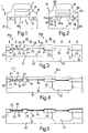
- Fig.s 1 and 2 show cross sections of EPROM and flash-EEPROM cells respectively.
- an EPROM cell As shown in Fig.1, an EPROM cell, indicated as a whole by 1, is formed in a substrate 2, in this case a P type, housing N+ type source and drain regions 3 and 4 separated by a channel region 5 formed by the substrate itself.
- a floating gate region 6 Over substrate 2, at channel 5, two gate regions are provided: a floating gate region 6 completely embedded in an oxide layer 8, and a control gate region 7.
- Gate region 6 is made of polycrystalline silicon; gate region 7 may be polysilicon or silicide (polysilicon and silicide); and the floating gate region is separated from the substrate by an oxide layer (gate oxide) 8a of a given thickness (typically 200 ⁇ ).
- a flash-EEPROM cell As shown in Fig.2, a flash-EEPROM cell, indicated as a whole by 15, is very similar to the Fig.1 EPROM cell, and is formed in a P type substrate 16 housing source and drain regions 17 and 18 separated by channel 19. In this case also, provision is made for a floating gate region 20 and a control gate region 21, both surrounded by an oxide layer 22. As compared with EPROM cell 1, however, the oxide layer 22a separating floating gate region 20 from substrate 16 and known as the tunnel oxide is much thinner, typically 100-130 ⁇ .
- source region 16 presents a graded junction with the substrate, and more specifically is formed in two parts: a heavily doped (N+) part 16a facing the larger surface 23 of the substrate, and a deeper, lightly doped (N-) part 16b surrounding part 16a on the sides not facing surface 23.
- the purpose of a graded junction is to enable the cell to better withstand the electrical stress to which it is subjected during erasing and programming, and may or may not be provided, depending on the operating conditions of the memory array.
- the thin tunnel oxide layer is essential for enabling electronic erasing (and programming) of the cell by Fowler-Nordheim tunneling between the substrate and floating gate.
- Flash-EEPROM fabrication involves specific steps for forming the tunnel oxide layer, due to its limited thickness, thus ruling out direct application of standard EPROM processes.
- Fig.3 shows an intermediate structure obtained by forming, in a P- type substrate 30, P type wells 31, N type wells 32, and P+ type enriched insulating regions 33 for the formation of channel stoppers, overlaid with thick field oxide regions 34.
- P-type substrate 30 P type wells 31, N type wells 32, and P+ type enriched insulating regions 33 for the formation of channel stoppers, overlaid with thick field oxide regions 34.
- a gate oxide layer 35 covering the active regions (where the circuit transistors and memory array cell are to be formed) and which elsewhere merges with field oxide layer 34. All the above layers and regions are obtained through standard process steps.
- An EPROM cell implant mask (EPM mask) is then formed for implanting boron ions in the channel area of the memory cell, as required for preventing punch-through of the substrate in the presence of strong electric fields, and for enhancing programming efficiency.
- Fig.3 shows the resist mask 36 covering the entire circuit portion (to the right in Fig.3 onwards, and indicated as a whole by 40a) and having a window 37 over the area in which the cell is to be formed (to the left in the drawings, and indicated 40b).
- Arrows 38 in Fig.3 indicate boron implantation for forming a P+ type layer 39 in the active region of the cell.
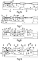
- Resist mask 36 is then removed; a first polycrystalline silicon layer is deposited (poly1, indicated by 41 in Fig.4 onwards); and poly1 41 is doped with POCl3 and subsequently shaped using a resist mask (42 in Fig.4) covering the entire circuit portion and which enables etching and removal of the exposed poly1 portions on either sides of memory area 40b, as shown in Fig.4.
- a dielectric layer (so-called interpoly dielectric 43) is then grown consisting, in this case, of a triple ONO (thermal oxide/CVD nitride/thermal oxide) layer, but which may also consist of a single oxide layer as shown in Fig.5 (showing the intermediate structure after growing dielectric layer 43).
- ONO thermal oxide/CVD nitride/thermal oxide
- a mask (array mask 44, Fig.6) is then deposited to cover cell array area 40b and leave circuit area 40a exposed; the exposed portions of dielectric layer 43 are removed to give the intermediate structure shown in Fig.6; mask 44 is removed; a further mask (so-called LVS mask not shown in the drawings) is deposited; and boron ions are implanted to adjust the threshold of the N channel circuit transistors and so form a P+ enriched region 45 (Fig.7).
- the above step also provides for reducing surface doping concentration in the active regions of the P channel transistors (in N well 32) and so adjusting the threshold to the desired value.
- a second polycrystalline silicon layer (poly2 47) is deposited.
- poly2 47 is deposited directly on to poly1 41 with which it merges to form a single polysilicon layer 48 (divided by the dotted line into two layers in the drawings for the sake of clarity), whereas, in the memory array area, it is separated from poly1 41 by dielectric layer 43.
- Poly2 47 is then doped with POCl3, and a layer of CVD silicide 49, e.g. tungsten silicide WSi2, is deposited to give the intermediate structure shown in Fig.7.
- a mask 50 (poly2 mask, Fig.8) is then formed for shaping the gate regions of the circuit transistors and the control gate regions of the array cells; and the exposed portions of the polysilicon layer (41 for the memory cells and 48 for the transistors) are removed by etching down to polysilicon layer 41 of the memory cells and the larger surface 51 of the substrate in circuit transistor area 40a, to give the intermediate structure shown in Fig.8.
- a further mask (transistor protection mask 54, Fig.9) is deposited to cover only and all of circuit area 40a; and the portions of poly1 left exposed by mask 50 or 54 are etched (to self-align the floating gate regions with the control gate regions).
- transistor protection mask 54 Fig.9
- arsenic is implanted, as shown by arrows 55 in Fig.9, so as to form, in the active area of the memory array cells and self-aligned with the floating gate and control gate regions, N type drain and source regions 56, as shown in the Fig.9 intermediate structure.
- the process according to the present invention comprises the same initial steps described above for forming the intermediate structure in Fig.3, which is again reproduced in Fig.10 for the sake of clarity. Any layers or regions in the present process identical to those of the known process described above are indicated using the same numbering system as in Figs. 3-9.
- Fig.10 shows a P- type substrate 30 housing P type wells 31 and N type wells 32; field insulating regions 34; channel stoppers 33; and a thin oxide layer 35'.
- the cell implant (EPM) mask 36 is already present, and, as in Fig.3, a cell implant (arrows 38') is performed for obtaining P type regions 60.
- the conditions of implant 38' differ from those of the EPROM process as per se known.
- gate oxide layer 35' is etched and removed from the cell region to give the intermediate structure shown in Fig.11, at which point, EPM mask 36 is removed and the wafer cleaned.
- the wafer is then oxidized to grow a thin oxide layer 61 directly on the surface of the substrate in the cell area, the oxidation parameters being so selected as to achieve the required characteristics, and particularly thickness, of the thin tunnel oxide layer. Oxidation also results in a slight increase in thickness of the gate oxide of the circuit transistors, as shown (exaggeratedly for the sake of clarity) by the dotted line in Fig.12 showing the original thickness of layer 35'.
- the gate oxide layer on the circuit portion is now indicated 35'' to take into account the increase in thickness, though it is substantially equivalent to layer 35 in the known process.
- the initial thickness of gate oxide layer 35' must therefore be so calculated as to allow for the tunnel oxidation increase and the slight reduction when cleaning the wafer (prior to forming the thin tunnel oxide).
- the known process flow is followed for depositing a first polycrystalline silicon layer 41; doping it with POCl3; forming poly1 mask 42; and shaping layer 41, as shown in Fig.13, and exactly as shown in Fig.4 except for thin oxide layer 61 and the different characteristics of region 60.
- This is followed by the steps shown in Figs. 5-9 relative to the known process, and which include depositing a dielectric layer; removing it from the circuit portion; depositing a second polysilicon layer; depositing a silicide layer; shaping the gate regions in the circuit transistor area and the control gate regions in the array; self-aligned shaping of the floating gate regions in the array; source and gate implants of the array cells and circuit transistors; and formation of the protection and connecting layers.
- the process according to the present invention thus provides for producing a flash-EEPROM memory array and associated transistors using the DPCC process, and so exploiting the intrinsic advantages, and in particular the experience and know-how, of the process for obtaining memories of known, reliable electric characteristics. Moreover, the possibility of producing flash-EEPROM memories using the DPCC process provides for producing two families of products (EPROM and flash-EEPROM memories) on the same fabrication line, with no significant differences and using the same machinery.
- the specific solution described also provides for producing flash-EEPROM memory cells with no need for specific masking and therefore at substantially the same cost as EPROM memories.
- CMOS and NMOS transistors regardless of the type of dielectric employed (ONO or single oxide layer), and regardless of the material of the control gate region (polysilicon or polycide, i.e. polysilicon and silicide).
Abstract

Description
- The present invention relates to a process for fabricating integrated devices including flash-EEPROM memories and transistors.
- Flash-EEPROM memories are Electrically Erasable Programmable Read Only Memories (EEPROMs) which combine the high density and low cost of EPROMs with the advantage of electrical erasability, and have recently become the most attractive of nonvolatile memories for their potential application in solid state disks for portable computers.
- Although different flash memory concepts have been developed, most flash manufacturers utilize the double-poly single-transistor cell which is very similar to a standard EPROM cell.
- Fig.s 1 and 2 show cross sections of EPROM and flash-EEPROM cells respectively.
- As shown in Fig.1, an EPROM cell, indicated as a whole by 1, is formed in a substrate 2, in this case a P type, housing N+ type source and
drain regions oxide layer 8, and a control gate region 7. Gate region 6 is made of polycrystalline silicon; gate region 7 may be polysilicon or silicide (polysilicon and silicide); and the floating gate region is separated from the substrate by an oxide layer (gate oxide) 8a of a given thickness (typically 200 Å). - As shown in Fig.2, a flash-EEPROM cell, indicated as a whole by 15, is very similar to the Fig.1 EPROM cell, and is formed in a
P type substrate 16 housing source anddrain regions 17 and 18 separated by channel 19. In this case also, provision is made for afloating gate region 20 and acontrol gate region 21, both surrounded by anoxide layer 22. As compared withEPROM cell 1, however, the oxide layer 22a separating floatinggate region 20 fromsubstrate 16 and known as the tunnel oxide is much thinner, typically 100-130 Å. In the specific embodiment shown,source region 16 presents a graded junction with the substrate, and more specifically is formed in two parts: a heavily doped (N+) part 16a facing thelarger surface 23 of the substrate, and a deeper, lightly doped (N-) part 16b surrounding part 16a on the sides not facingsurface 23. - The purpose of a graded junction is to enable the cell to better withstand the electrical stress to which it is subjected during erasing and programming, and may or may not be provided, depending on the operating conditions of the memory array. The thin tunnel oxide layer, on the other hand, is essential for enabling electronic erasing (and programming) of the cell by Fowler-Nordheim tunneling between the substrate and floating gate.
- Flash-EEPROM fabrication involves specific steps for forming the tunnel oxide layer, due to its limited thickness, thus ruling out direct application of standard EPROM processes.
- The present applicant has developed and patented an EPROM process whereby the second polysilicon layer is deposited directly on the first in the circuit transistor area, for forming the gate regions of the transistors (and which thus, unlike other known processes, does not require removal of the first polysilicon layer in the circuit area). This process, protected by Patent US-A-4.719.184 issued on 12.1.88 and known as DPCC (Shorted Double Poly) provides for advantages in terms of reliability and the number of masks required.
- It is an object of the present invention to provide a process for fabricating integrated devices, designed to exploit the basic principle and so achieve the technical advantages of the known DPCC process.
- According to the present invention, there is provided a process for fabricating integrated devices including flash-EEPROM memories and transistors, as claimed in
Claim 1. - A preferred, non-limiting embodiment of the present invention will be described by way of example with reference to the accompanying drawings, in which:
- Fig.1 shows a cross section of a known EPROM cell;
- Fig.2 shows a cross section, as in Fig.1, of a known flash-EEPROM cell;
- Fig.s 3-9 show cross sections of a silicon wafer relative to various steps in the known DPCC process for fabricating an integrated device including an EPROM memory and transistors;
- Fig.s 10-13 show cross sections of a silicon wafer relative to various steps in the fabrication of an integrated device including a flash-EEPROM memory and transistors according to the present invention.
- With reference to Fig.s 3-9, a description will first be given of the known DPCC process for fabricating EPROM cells and circuit transistors according to Patent US-A-4.719.184 mentioned above. In particular, the following description relates to various steps in a CMOS DPCC process for fabricating an EPROM memory cell and CMOS transistors.
- Fig.3 shows an intermediate structure obtained by forming, in a P-
type substrate 30,P type wells 31,N type wells 32, and P+ type enrichedinsulating regions 33 for the formation of channel stoppers, overlaid with thickfield oxide regions 34. Oversubstrate 30, provision is also made for agate oxide layer 35 covering the active regions (where the circuit transistors and memory array cell are to be formed) and which elsewhere merges withfield oxide layer 34. All the above layers and regions are obtained through standard process steps. - An EPROM cell implant mask (EPM mask) is then formed for implanting boron ions in the channel area of the memory cell, as required for preventing punch-through of the substrate in the presence of strong electric fields, and for enhancing programming efficiency.
- This step is shown in Fig.3, which shows the
resist mask 36 covering the entire circuit portion (to the right in Fig.3 onwards, and indicated as a whole by 40a) and having awindow 37 over the area in which the cell is to be formed (to the left in the drawings, and indicated 40b).Arrows 38 in Fig.3 indicate boron implantation for forming aP+ type layer 39 in the active region of the cell. -
Resist mask 36 is then removed; a first polycrystalline silicon layer is deposited (poly1, indicated by 41 in Fig.4 onwards); andpoly1 41 is doped with POCl₃ and subsequently shaped using a resist mask (42 in Fig.4) covering the entire circuit portion and which enables etching and removal of the exposed poly1 portions on either sides ofmemory area 40b, as shown in Fig.4. - A dielectric layer (so-called interpoly dielectric 43) is then grown consisting, in this case, of a triple ONO (thermal oxide/CVD nitride/thermal oxide) layer, but which may also consist of a single oxide layer as shown in Fig.5 (showing the intermediate structure after growing dielectric layer 43).
- A mask (
array mask 44, Fig.6) is then deposited to covercell array area 40b andleave circuit area 40a exposed; the exposed portions ofdielectric layer 43 are removed to give the intermediate structure shown in Fig.6;mask 44 is removed; a further mask (so-called LVS mask not shown in the drawings) is deposited; and boron ions are implanted to adjust the threshold of the N channel circuit transistors and so form a P+ enriched region 45 (Fig.7). At the same time, the above step also provides for reducing surface doping concentration in the active regions of the P channel transistors (in N well 32) and so adjusting the threshold to the desired value. - Following removal of the LVS mask (not shown), a second polycrystalline silicon layer (poly2 47) is deposited. As shown in Fig.7, in
circuit area 40a,poly2 47 is deposited directly on topoly1 41 with which it merges to form a single polysilicon layer 48 (divided by the dotted line into two layers in the drawings for the sake of clarity), whereas, in the memory array area, it is separated frompoly1 41 bydielectric layer 43.Poly2 47 is then doped with POCl₃, and a layer ofCVD silicide 49, e.g. tungsten silicide WSi₂, is deposited to give the intermediate structure shown in Fig.7. - A mask 50 (poly2 mask, Fig.8) is then formed for shaping the gate regions of the circuit transistors and the control gate regions of the array cells; and the exposed portions of the polysilicon layer (41 for the memory cells and 48 for the transistors) are removed by etching down to
polysilicon layer 41 of the memory cells and thelarger surface 51 of the substrate incircuit transistor area 40a, to give the intermediate structure shown in Fig.8. - On top of the
poly2 mask 50, a further mask (transistor protection mask 54, Fig.9) is deposited to cover only and all ofcircuit area 40a; and the portions of poly1 left exposed bymask mask arrows 55 in Fig.9, so as to form, in the active area of the memory array cells and self-aligned with the floating gate and control gate regions, N type drain andsource regions 56, as shown in the Fig.9 intermediate structure. - The rest of the process then follows the standard CMOS flow, for forming the source and drain regions of the circuit transistors, the component protection layers, and the connections.
- One embodiment of the process according to the present invention will now be described with reference to Figs. 10-13 and relative to the formation of a flash-EEPROM cell and a pair of CMOS complementary transistors.
- The process according to the present invention comprises the same initial steps described above for forming the intermediate structure in Fig.3, which is again reproduced in Fig.10 for the sake of clarity. Any layers or regions in the present process identical to those of the known process described above are indicated using the same numbering system as in Figs. 3-9.
- Fig.10 shows a P-
type substrate 30 housingP type wells 31 andN type wells 32;field insulating regions 34;channel stoppers 33; and a thin oxide layer 35'. As explained in more detail later on, for obtaining the required finish thickness of layer 35', a number of parameters must be adjusted as compared with the known process described with reference to Figs. 3-9. In Fig.10, the cell implant (EPM)mask 36 is already present, and, as in Fig.3, a cell implant (arrows 38') is performed for obtainingP type regions 60. In view of the different characteristics of the EPROM cells formed in the Fig.3-9 process and the flash-EEPROM cells being produced here, the conditions of implant 38' differ from those of the EPROM process as per se known. - Using the same cell implant (EPM)
mask 36, gate oxide layer 35' is etched and removed from the cell region to give the intermediate structure shown in Fig.11, at which point,EPM mask 36 is removed and the wafer cleaned. The wafer is then oxidized to grow athin oxide layer 61 directly on the surface of the substrate in the cell area, the oxidation parameters being so selected as to achieve the required characteristics, and particularly thickness, of the thin tunnel oxide layer. Oxidation also results in a slight increase in thickness of the gate oxide of the circuit transistors, as shown (exaggeratedly for the sake of clarity) by the dotted line in Fig.12 showing the original thickness of layer 35'. The gate oxide layer on the circuit portion is now indicated 35'' to take into account the increase in thickness, though it is substantially equivalent tolayer 35 in the known process. - As stated above, the initial thickness of gate oxide layer 35' must therefore be so calculated as to allow for the tunnel oxidation increase and the slight reduction when cleaning the wafer (prior to forming the thin tunnel oxide).
- At this point, the known process flow is followed for depositing a first
polycrystalline silicon layer 41; doping it with POCl₃; formingpoly1 mask 42; and shapinglayer 41, as shown in Fig.13, and exactly as shown in Fig.4 except forthin oxide layer 61 and the different characteristics ofregion 60. This is followed by the steps shown in Figs. 5-9 relative to the known process, and which include depositing a dielectric layer; removing it from the circuit portion; depositing a second polysilicon layer; depositing a silicide layer; shaping the gate regions in the circuit transistor area and the control gate regions in the array; self-aligned shaping of the floating gate regions in the array; source and gate implants of the array cells and circuit transistors; and formation of the protection and connecting layers. - The process according to the present invention thus provides for producing a flash-EEPROM memory array and associated transistors using the DPCC process, and so exploiting the intrinsic advantages, and in particular the experience and know-how, of the process for obtaining memories of known, reliable electric characteristics. Moreover, the possibility of producing flash-EEPROM memories using the DPCC process provides for producing two families of products (EPROM and flash-EEPROM memories) on the same fabrication line, with no significant differences and using the same machinery.
- The specific solution described also provides for producing flash-EEPROM memory cells with no need for specific masking and therefore at substantially the same cost as EPROM memories.
- To those skilled in the art it will be clear that changes may be made to the process as described and illustrated herein without, however, departing from the scope of the present invention. In particular, the process described is applicable to devices including CMOS and NMOS transistors, regardless of the type of dielectric employed (ONO or single oxide layer), and regardless of the material of the control gate region (polysilicon or polycide, i.e. polysilicon and silicide).
Claims (6)
- A process for fabricating flash-EEPROM nonvolatile memory cells and circuit transistors from a substrate having a larger surface (51) and defining cell areas (40b) in which to form the memory cells, and transistor areas (40a) in which to form the circuit transistors; characterized by the fact that it comprises, in combination, the steps of:- growing field oxide regions (34) on predetermined portions of said larger surface (51) of said substrate (30);- forming a gate oxide layer (35') on said larger surface of said substrate, in said transistor areas (40a);- forming a thin tunnel oxide layer (61) on said larger surface of said substrate, in said cell areas (40b);- depositing a first polycrystalline silicon layer (41);- selectively removing portions of said first polycrystalline silicon layer (41) at the sides of said cell areas (40b) and said transistor areas (40a);- depositing a dielectric material layer (43);- removing said dielectric material layer (43) from said transistor areas (40a);- depositing a second polycrystalline silicon layer (47);- masking and selectively removing said second polycrystalline silicon layer (47) and said underlying dielectric layer (43) at the sides of said cell areas (40b), and said second and first polycrystalline silicon layers (47, 41) and said gate oxide layer (35) at the sides of said transistor areas (40a), so as to leave the source and drain areas of said circuit transistors exposed; and- using the same mask, selectively removing said first polycrystalline silicon layer (41) and said thin tunnel oxide layer (61) at the sides of said cell areas (40b), so as to leave the source and drain areas of the cells exposed.
- A process as claimed in Claim 1, characterized by the fact that said step of forming a thin tunnel oxide layer (61) is performed after said step of forming a gate oxide layer (35').
- A process as claimed in Claim 2, characterized by the fact that said step of forming a gate oxide layer comprises the steps of growing a gate oxide layer (35') over the whole of said larger surface of said substrate (30) and selectively removing portions of said gate oxide layer from said cell areas (40b).
- A process as claimed in Claim 3, characterized by the fact that, following said step of growing a gate oxide layer (35') over the whole of said larger surface of said substrate (30), and prior to said step of forming a thin tunnel oxide layer (61), there are performed the steps of: masking said larger surface of said substrate for forming a doping mask (36) covering said transistor areas (40a) and exposing said cell areas (40b); doping (38) said cell areas (40b) with conductivity-modifying ions and using said doping mask (36); and by the fact that said step of selectively removing portions of said gate oxide layer (35') from said cell areas (40b) is performed using said doping mask (36).
- A process as claimed in Claim 4, characterized by the fact that said step of doping (38) said cell area (40b) is performed through said gate oxide layer (35').
- A process as claimed in Claim 4 or 5, characterized by the fact that said doping mask (36) is removed following said step of selectively removing portions of said gate oxide layer (35') from said cell area (40b); and by the fact that said step of forming a thin tunnel oxide layer (61) is performed over the whole surface of said substrate (30), so as to increase the thickness of said gate oxide layer (35'') in said transistor areas (40a).
Priority Applications (4)
| Application Number | Priority Date | Filing Date | Title |
|---|---|---|---|
| EP93830050A EP0610643B1 (en) | 1993-02-11 | 1993-02-11 | EEPROM cell and peripheral MOS transistor |
| DE69313816T DE69313816T2 (en) | 1993-02-11 | 1993-02-11 | EEPROM cell and peripheral MOS transistor |
| JP6016744A JPH077093A (en) | 1993-02-11 | 1994-02-10 | Manufacture of non-volatile memory cell of flash eeprom and circuit transistor |
| US08/195,369 US5637520A (en) | 1993-02-11 | 1994-02-10 | Process for fabricating integrated devices including flash-EEPROM memories and transistors |
Applications Claiming Priority (1)
| Application Number | Priority Date | Filing Date | Title |
|---|---|---|---|
| EP93830050A EP0610643B1 (en) | 1993-02-11 | 1993-02-11 | EEPROM cell and peripheral MOS transistor |
Publications (2)
| Publication Number | Publication Date |
|---|---|
| EP0610643A1 true EP0610643A1 (en) | 1994-08-17 |
| EP0610643B1 EP0610643B1 (en) | 1997-09-10 |
Family
ID=8215116
Family Applications (1)
| Application Number | Title | Priority Date | Filing Date |
|---|---|---|---|
| EP93830050A Expired - Lifetime EP0610643B1 (en) | 1993-02-11 | 1993-02-11 | EEPROM cell and peripheral MOS transistor |
Country Status (4)
| Country | Link |
|---|---|
| US (1) | US5637520A (en) |
| EP (1) | EP0610643B1 (en) |
| JP (1) | JPH077093A (en) |
| DE (1) | DE69313816T2 (en) |
Cited By (2)
| Publication number | Priority date | Publication date | Assignee | Title |
|---|---|---|---|---|
| EP0822598A1 (en) * | 1996-07-30 | 1998-02-04 | Nec Corporation | Single-chip contact-less read-only memory (rom) device and the method for fabricating the device |
| EP1852909A1 (en) * | 2006-05-05 | 2007-11-07 | Austriamicrosystems AG | Process for integrating a non-volatile memory cell into a HV CMOS process |
Families Citing this family (17)
| Publication number | Priority date | Publication date | Assignee | Title |
|---|---|---|---|---|
| US5960274A (en) * | 1996-08-19 | 1999-09-28 | Advanced Micro Devices, Inc. | Oxide formation process for manufacturing programmable logic device |
| US6033943A (en) * | 1996-08-23 | 2000-03-07 | Advanced Micro Devices, Inc. | Dual gate oxide thickness integrated circuit and process for making same |
| US6051510A (en) * | 1997-05-02 | 2000-04-18 | Advanced Micro Devices, Inc. | Method of using a hard mask to grow dielectrics with varying characteristics |
| US6037224A (en) * | 1997-05-02 | 2000-03-14 | Advanced Micro Devices, Inc. | Method for growing dual oxide thickness using nitrided oxides for oxidation suppression |
| US6207991B1 (en) | 1998-03-20 | 2001-03-27 | Cypress Semiconductor Corp. | Integrated non-volatile and CMOS memories having substantially the same thickness gates and methods of forming the same |
| US6124157A (en) * | 1998-03-20 | 2000-09-26 | Cypress Semiconductor Corp. | Integrated non-volatile and random access memory and method of forming the same |
| FR2778018B1 (en) * | 1998-04-28 | 2000-06-23 | Sgs Thomson Microelectronics | METHOD FOR MANUFACTURING EEPROM DEVICES |
| KR100475033B1 (en) * | 1998-06-08 | 2005-05-27 | 삼성전자주식회사 | Manufacturing method of nonvolatile memory device |
| TW432536B (en) * | 1998-07-16 | 2001-05-01 | United Microelectronics Corp | Method of fabricating an electrically erasable and programmable read-only memory (EEPROM) with improved quality for the tunneling oxide layer therein |
| US6096664A (en) * | 1998-08-06 | 2000-08-01 | Siemens Aktiengesellschaft | Method of manufacturing semiconductor structures including a pair of MOSFETs |
| US6235586B1 (en) * | 1999-07-13 | 2001-05-22 | Advanced Micro Devices, Inc. | Thin floating gate and conductive select gate in situ doped amorphous silicon material for NAND type flash memory device applications |
| US6147008A (en) * | 1999-11-19 | 2000-11-14 | Chartered Semiconductor Manufacturing Ltd. | Creation of multiple gate oxide with high thickness ratio in flash memory process |
| US6979619B1 (en) * | 2000-06-15 | 2005-12-27 | Advanced Micro Devices, Inc. | Flash memory device and a method of fabrication thereof |
| JP2002100688A (en) * | 2000-09-22 | 2002-04-05 | Oki Electric Ind Co Ltd | Method of manufacturing nonvolatile semiconductor memory |
| US7621293B2 (en) * | 2001-04-05 | 2009-11-24 | Fisher Controls International Llc | Versatile emergency shutdown device controller implementing a pneumatic test for a system instrument device |
| KR100426484B1 (en) * | 2001-12-22 | 2004-04-14 | 주식회사 하이닉스반도체 | Flash memory cell and method of manufacturing the same |
| US6846714B1 (en) * | 2002-10-03 | 2005-01-25 | Lattice Semiconductor Corporation | Voltage limited EEPROM device and process for fabricating the device |
Citations (5)
| Publication number | Priority date | Publication date | Assignee | Title |
|---|---|---|---|---|
| DE3107543A1 (en) * | 1980-02-27 | 1981-12-24 | Hitachi, Ltd., Tokyo | INTEGRATED SEMICONDUCTOR CIRCUIT DEVICE AND METHOD FOR THEIR PRODUCTION |
| EP0106617A2 (en) * | 1982-10-05 | 1984-04-25 | Fujitsu Limited | Method for fabricating an EEPROM |
| GB2167602A (en) * | 1984-11-26 | 1986-05-29 | Sgs Microelettronica Spa | Process for the fabrication of integrated structures including nonvolatile memory cells and transistors |
| EP0244367A2 (en) * | 1986-04-21 | 1987-11-04 | SGS MICROELETTRONICA S.p.A. | Mos type integrated semiconductor device with nonuniform thickness of gate oxide and process for fabricating it |
| EP0305741A2 (en) * | 1987-07-31 | 1989-03-08 | Kabushiki Kaisha Toshiba | Semiconductor device with floating gate |
Family Cites Families (11)
| Publication number | Priority date | Publication date | Assignee | Title |
|---|---|---|---|---|
| DE107543C (en) * | ||||
| GB167602A (en) * | 1920-05-17 | 1921-08-17 | Thomas Lauge Eggleston | Improvements in airplane supporting planes or wings |
| JPS5974677A (en) * | 1982-10-22 | 1984-04-27 | Ricoh Co Ltd | Semiconductor device and manufacture thereof |
| US5086008A (en) * | 1988-02-29 | 1992-02-04 | Sgs-Thomson Microelectronics S.R.L. | Process for obtaining high-voltage N channel transistors particularly for EEPROM memories with CMOS technology |
| NL8802219A (en) * | 1988-09-09 | 1990-04-02 | Philips Nv | METHOD FOR MANUFACTURING A SILICON BODY SEMICONDUCTOR DEVICE CONTAINING SEMICON IMPLANTS FOR SEMICONDUCTOR AREAS. |
| IT1232354B (en) * | 1989-09-04 | 1992-01-28 | Sgs Thomson Microelectronics | PROCEDURE FOR THE CREATION OF EEPROM MEMORY CELLS AT A SINGLE LEVEL OF POLYSILICIO AND THIN OXIDE USING DIFFERENTIAL OXIDATION. |
| US5215934A (en) * | 1989-12-21 | 1993-06-01 | Tzeng Jyh Cherng J | Process for reducing program disturbance in eeprom arrays |
| US5254489A (en) * | 1990-10-18 | 1993-10-19 | Nec Corporation | Method of manufacturing semiconductor device by forming first and second oxide films by use of nitridation |
| JP3548984B2 (en) * | 1991-11-14 | 2004-08-04 | 富士通株式会社 | Method for manufacturing semiconductor device |
| US5316981A (en) * | 1992-10-09 | 1994-05-31 | Advanced Micro Devices, Inc. | Method for achieving a high quality thin oxide using a sacrificial oxide anneal |
| US5498577A (en) * | 1994-07-26 | 1996-03-12 | Advanced Micro Devices, Inc. | Method for fabricating thin oxides for a semiconductor technology |
-
1993
- 1993-02-11 DE DE69313816T patent/DE69313816T2/en not_active Expired - Fee Related
- 1993-02-11 EP EP93830050A patent/EP0610643B1/en not_active Expired - Lifetime
-
1994
- 1994-02-10 US US08/195,369 patent/US5637520A/en not_active Expired - Lifetime
- 1994-02-10 JP JP6016744A patent/JPH077093A/en active Pending
Patent Citations (5)
| Publication number | Priority date | Publication date | Assignee | Title |
|---|---|---|---|---|
| DE3107543A1 (en) * | 1980-02-27 | 1981-12-24 | Hitachi, Ltd., Tokyo | INTEGRATED SEMICONDUCTOR CIRCUIT DEVICE AND METHOD FOR THEIR PRODUCTION |
| EP0106617A2 (en) * | 1982-10-05 | 1984-04-25 | Fujitsu Limited | Method for fabricating an EEPROM |
| GB2167602A (en) * | 1984-11-26 | 1986-05-29 | Sgs Microelettronica Spa | Process for the fabrication of integrated structures including nonvolatile memory cells and transistors |
| EP0244367A2 (en) * | 1986-04-21 | 1987-11-04 | SGS MICROELETTRONICA S.p.A. | Mos type integrated semiconductor device with nonuniform thickness of gate oxide and process for fabricating it |
| EP0305741A2 (en) * | 1987-07-31 | 1989-03-08 | Kabushiki Kaisha Toshiba | Semiconductor device with floating gate |
Cited By (3)
| Publication number | Priority date | Publication date | Assignee | Title |
|---|---|---|---|---|
| EP0822598A1 (en) * | 1996-07-30 | 1998-02-04 | Nec Corporation | Single-chip contact-less read-only memory (rom) device and the method for fabricating the device |
| US6121670A (en) * | 1996-07-30 | 2000-09-19 | Nec Corporation | Single-chip contact-less read-only memory (ROM) device and the method for fabricating the device |
| EP1852909A1 (en) * | 2006-05-05 | 2007-11-07 | Austriamicrosystems AG | Process for integrating a non-volatile memory cell into a HV CMOS process |
Also Published As
| Publication number | Publication date |
|---|---|
| JPH077093A (en) | 1995-01-10 |
| EP0610643B1 (en) | 1997-09-10 |
| US5637520A (en) | 1997-06-10 |
| DE69313816T2 (en) | 1998-03-26 |
| DE69313816D1 (en) | 1997-10-16 |
Similar Documents
| Publication | Publication Date | Title |
|---|---|---|
| EP0610643B1 (en) | EEPROM cell and peripheral MOS transistor | |
| US5668034A (en) | Process for fabricating a high voltage MOS transistor for flash EEPROM applications having a uni-sided lightly doped drain | |
| US6514830B1 (en) | Method of manufacturing high voltage transistor with modified field implant mask | |
| US6627928B2 (en) | Method of manufacturing an integrated circuit, for integrating an electrically programmable, non-volatile memory and high-performance logic circuitry in the same semiconductor chip | |
| US5081054A (en) | Fabrication process for programmable and erasable MOS memory device | |
| US5429969A (en) | Process for forming electrically programmable read-only memory cell with a merged select/control gate | |
| US5913120A (en) | Process for fabricating integrated devices including nonvolatile memories and transistors with tunnel oxide protection | |
| US6159795A (en) | Low voltage junction and high voltage junction optimization for flash memory | |
| US20010012662A1 (en) | A new structure to fabricate split-gate with self-aligned source and self-aligned floating gate to control gate | |
| WO1995025350A1 (en) | Eeprom cell with the drain diffusion region self-aligned to the tunnel oxide region and method of manufacture | |
| US6624015B2 (en) | Method for manufacturing electronic devices having non-volatile memory cells and LV transistors with salicided junctions | |
| US6177315B1 (en) | Method of fabricating a high density EEPROM array | |
| KR20000073371A (en) | Semiconductor memory device and fabricating method thereof | |
| US6396101B2 (en) | Method for manufacturing electronic devices comprising non-volatile memory cells and LV transistors with salicided junctions | |
| US6355523B1 (en) | Manufacturing process for making single polysilicon level flash EEPROM cell | |
| KR100284739B1 (en) | Method of manufacturing non-volatile memory device | |
| JP2000133729A (en) | Electronic device and manufacture thereof including nonvolatile memory cell subjected to non-salicide processing, high-voltage transistor subjected thereto, and junction low-voltage transistor subjected to salicide processing | |
| US6268247B1 (en) | Memory cell of the EEPROM type having its threshold set by implantation, and fabrication method | |
| US6806143B2 (en) | Self-aligned source pocket for flash memory cells | |
| US6025229A (en) | Method of fabricating split-gate source side injection flash memory array | |
| US5527727A (en) | Method of manufacturing split gate EEPROM cells | |
| US6165847A (en) | Nonvolatile semiconductor memory device and method for manufacturing the same | |
| US6329254B1 (en) | Memory cell of the EEPROM type having its threshold adjusted by implantation, and fabrication method | |
| US6097057A (en) | Memory cell for EEPROM devices, and corresponding fabricating process | |
| US20020000605A1 (en) | Method of fabricating high-coupling ratio split gate flash memory cell array |
Legal Events
| Date | Code | Title | Description |
|---|---|---|---|
| PUAI | Public reference made under article 153(3) epc to a published international application that has entered the european phase |
Free format text: ORIGINAL CODE: 0009012 |
|
| AK | Designated contracting states |
Kind code of ref document: A1 Designated state(s): DE FR GB IT |
|
| 17P | Request for examination filed |
Effective date: 19940330 |
|
| GRAG | Despatch of communication of intention to grant |
Free format text: ORIGINAL CODE: EPIDOS AGRA |
|
| 17Q | First examination report despatched |
Effective date: 19961120 |
|
| GRAH | Despatch of communication of intention to grant a patent |
Free format text: ORIGINAL CODE: EPIDOS IGRA |
|
| GRAH | Despatch of communication of intention to grant a patent |
Free format text: ORIGINAL CODE: EPIDOS IGRA |
|
| GRAA | (expected) grant |
Free format text: ORIGINAL CODE: 0009210 |
|
| AK | Designated contracting states |
Kind code of ref document: B1 Designated state(s): DE FR GB IT |
|
| ITF | It: translation for a ep patent filed |
Owner name: STUDIO TORTA S.R.L. |
|
| REF | Corresponds to: |
Ref document number: 69313816 Country of ref document: DE Date of ref document: 19971016 |
|
| ET | Fr: translation filed | ||
| PLBE | No opposition filed within time limit |
Free format text: ORIGINAL CODE: 0009261 |
|
| STAA | Information on the status of an ep patent application or granted ep patent |
Free format text: STATUS: NO OPPOSITION FILED WITHIN TIME LIMIT |
|
| RAP4 | Party data changed (patent owner data changed or rights of a patent transferred) |
Owner name: STMICROELECTRONICS S.R.L. |
|
| 26N | No opposition filed | ||
| REG | Reference to a national code |
Ref country code: GB Ref legal event code: IF02 |
|
| PGFP | Annual fee paid to national office [announced via postgrant information from national office to epo] |
Ref country code: DE Payment date: 20020227 Year of fee payment: 10 |
|
| PG25 | Lapsed in a contracting state [announced via postgrant information from national office to epo] |
Ref country code: DE Free format text: LAPSE BECAUSE OF NON-PAYMENT OF DUE FEES Effective date: 20030902 |
|
| PGFP | Annual fee paid to national office [announced via postgrant information from national office to epo] |
Ref country code: FR Payment date: 20040210 Year of fee payment: 12 |
|
| PGFP | Annual fee paid to national office [announced via postgrant information from national office to epo] |
Ref country code: GB Payment date: 20040211 Year of fee payment: 12 |
|
| PG25 | Lapsed in a contracting state [announced via postgrant information from national office to epo] |
Ref country code: IT Free format text: LAPSE BECAUSE OF NON-PAYMENT OF DUE FEES;WARNING: LAPSES OF ITALIAN PATENTS WITH EFFECTIVE DATE BEFORE 2007 MAY HAVE OCCURRED AT ANY TIME BEFORE 2007. THE CORRECT EFFECTIVE DATE MAY BE DIFFERENT FROM THE ONE RECORDED. Effective date: 20050211 Ref country code: GB Free format text: LAPSE BECAUSE OF NON-PAYMENT OF DUE FEES Effective date: 20050211 |
|
| GBPC | Gb: european patent ceased through non-payment of renewal fee |
Effective date: 20050211 |
|
| PG25 | Lapsed in a contracting state [announced via postgrant information from national office to epo] |
Ref country code: FR Free format text: LAPSE BECAUSE OF NON-PAYMENT OF DUE FEES Effective date: 20051031 |
|
| REG | Reference to a national code |
Ref country code: FR Ref legal event code: ST Effective date: 20051031 |