EP0608536B1 - Arc welding apparatus with semiconducting switches having a central connexion - Google Patents
Arc welding apparatus with semiconducting switches having a central connexion Download PDFInfo
- Publication number
- EP0608536B1 EP0608536B1 EP93120107A EP93120107A EP0608536B1 EP 0608536 B1 EP0608536 B1 EP 0608536B1 EP 93120107 A EP93120107 A EP 93120107A EP 93120107 A EP93120107 A EP 93120107A EP 0608536 B1 EP0608536 B1 EP 0608536B1
- Authority
- EP
- European Patent Office
- Prior art keywords
- current paths
- arc welding
- current
- welding apparatus
- rectifier
- Prior art date
- Legal status (The legal status is an assumption and is not a legal conclusion. Google has not performed a legal analysis and makes no representation as to the accuracy of the status listed.)
- Expired - Lifetime
Links
Images


Classifications
-
- B—PERFORMING OPERATIONS; TRANSPORTING
- B23—MACHINE TOOLS; METAL-WORKING NOT OTHERWISE PROVIDED FOR
- B23K—SOLDERING OR UNSOLDERING; WELDING; CLADDING OR PLATING BY SOLDERING OR WELDING; CUTTING BY APPLYING HEAT LOCALLY, e.g. FLAME CUTTING; WORKING BY LASER BEAM
- B23K9/00—Arc welding or cutting
- B23K9/10—Other electric circuits therefor; Protective circuits; Remote controls
- B23K9/1006—Power supply
- B23K9/1043—Power supply characterised by the electric circuit
- B23K9/1056—Power supply characterised by the electric circuit by using digital means
Definitions
- the invention relates to an arc welding device with an AC-fed rectifier, which feeds an intermediate circuit, a current transformer clocked on the primary side, to which two parallel current paths are assigned on the secondary side, of which the welding process can be acted on with a time delay in the opposite direction, each of the two current paths being a free-wheeling diode, a rectifier diode and has a controllable semiconductor switch, the switching cycle of which determines the working frequency of the arc welding device in AC operation.
- Such a welding device is known from German Patent 38 03 447.
- This known welding device enables the welding processes to be supplied with both DC and DC Alternating current.
- AC welding is technologically more advantageous in special applications because, for example, in aluminum welding, the oxide layer formed in one current direction during a welding period is broken up again by the opposite current in the following period.
- a mechanical changeover switch is additionally provided, in the first position for DC operation, both current paths feed the welding process together and in the second position, which determines AC operation, the first semiconductor switch carries the current of the first current path and the second semiconductor switch carries the current of the second current path .
- Such a mechanical switch has drawbacks due to its finite service life in continuous operation.
- an arc welding device in which a bridge circuit formed from four semiconductor switches is provided in the secondary circuit, both direct current and alternating current operation being made possible by the corresponding control of the semiconductor switches.
- This solution has the disadvantage that power dissipation occurs at each of the four semiconductor switches during operation.
- a welding device of the type mentioned is also known from DE-OS 40 11 461.
- This welding device always requires at least two separate current transformers to supply the two secondary-side current paths, of which only one is always conductive in one phase. This means that two converters must always be used to maintain the function of this circuit.
- the invention has for its object to further develop an arc welding device of the type mentioned in such a way that on the one hand it is simplified in terms of circuitry and on the other hand it is optimized with regard to power loss.
- each of the two current paths is fed by spatially separate secondary windings which are acted upon by a common primary winding and in that in each of the two secondary-side current paths a separately controllable semiconductor switch is provided, which are linked together in a center circuit, the semiconductor switches being controllable such that either only one of the two current paths is conductive (DC output) or the two current paths are alternately conductive (AC output).
- this object is achieved in that the two current paths are connected to a common secondary winding, the primary winding being fed by primary switches located in a bridge circuit in such a way that alternating secondary voltages are available and that a separate one is present in each of the two secondary-side current paths controllable semiconductor switches are provided which are linked together in a center circuit, the semiconductor switches being controllable in such a way that either only one of the two current paths is conductive (DC output) or the two current paths are alternately conductive (AC output).
- the invention is characterized in that the circuit complexity can be reduced by the fact that now only one converter is required.
- the arrangement and the control of the semiconductor switches ensure that only one of the two current paths is always activated and the other is correspondingly hidden.
- the two variants differ in that, according to the first variant, two separate secondary windings fed by a common primary winding are provided, while according to the second variant a common secondary winding is provided, which receives alternately opposite polarity by clocking on the primary side. Both variants have in common that a single converter is always sufficient.
- the invention is further characterized in that both the operating mode (direct current or alternating current) itself and in the "alternating current" operating mode, the working frequency for the supply of the welding process can be determined solely by controlling the secondary-side semiconductor switches. Additional switching means, such as a mechanical switch, can therefore be omitted.
- the "direct current" operating mode alternatively only one of the two semiconductor switches is continuously conductive and the other is permanently blocked. This results in loss power only in the current path containing the conductive semiconductor switch, while the other current path generates no losses.
- the semiconductor switches are alternately conductive, clocked at the operating frequency, with the current path containing the other switch in turn causing no power loss during the conductive phase of the one switch, and vice versa.
- the second variant has the further advantage that at least one winding can be saved compared to the first variant. This also further reduces the complexity of the circuitry.
- the advantage of the first variant of the invention is that free-wheeling diodes, rectifier diodes and secondary-side semiconductor switches can be arranged on a common heat sink. Compared to the known solution, a heat sink can be saved here.
- the current paths are preferably conductive alternately over non-overlapping time intervals.
- the primary winding for feeding the two spatially separate secondary windings is also divided into two partial windings, which are fed by two clocked primary switches lying in series with it.
- the solution according to the invention can be applied not only to the so-called inverter current sources, but also to conventional current sources with an operating frequency of 50 Hz, which consist of a mains transformer and a conventional three-phase rectifier.
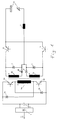
- Fig. 1 shows a rectifier 1 fed by a single or three-phase network, which can be equipped with both controlled and uncontrolled flow control valves.
- the rectifier 1 feeds a capacitor 2 forming an intermediate circuit, which in turn supplies the current transformer 5a, 5b, 5c arranged downstream of it.
- the primary winding 5a of the current transformer is driven in a clocked manner by primary semiconductor switches 4a, 4b.
- freewheeling diodes 3a, 3b are provided, which cause the current transformer 5a, 5b, 5c to be demagnetized during those time intervals in which the transformer is not clocked by the semiconductor switches 4a, 4b.
- the secondary side of the current transformer is formed by two separate secondary windings 5b, 5c, the winding sense of which is the same as that of the corresponding points is shown.
- a first current path is connected to the upper secondary winding 5b and consists of the components rectifier diode 6, controlled semiconductor switch 10, welding process 13, smoothing choke 12 and freewheeling diode 7.
- a second current path is connected to the lower secondary winding 5c and consists of the elements rectifier diode 8, smoothing inductor 12, welding process 13, controlled semiconductor switch 11 and free-wheeling diode 9.
- the two current paths are switched such that the welding process 13 flows through in a first current direction when the upper current path is applied and in the opposite, second current direction when the lower current path is applied.
- the method of operation of the circuit according to the invention for the arc welding device according to FIG. 1 is now as follows:
- the current transformer 5a, 5b, 5c operates by clocking the primary-side semiconductor switches 4a, 4b with a clock frequency of approximately 20 kHz.
- the secondary voltages are rectified via the rectifier diodes 6 and 8, so that two DC voltages are available for each of the two current paths at their output. If the arc welding device is to be supplied with direct current, only one of the two semiconductor switches 10, 11 on the secondary side is conductive, while the other is permanently blocked. For example, if this is switch 10, only current flows through the welding process in the first direction. In this operating state, no power loss can occur in the current path that is not activated.
- the secondary-side semiconductor switches 10, 11 are clocked by a control device (not shown in more detail) in such a way that they are alternately conductive.
- the clocking takes place in the desired operating frequency for the welding process, for example 200 Hz. Since this frequency is significantly lower than the clock frequency of the current transformer, the DC voltage available at the rectifier diodes 6 and 8 is transmitted to the welding process almost undeformed. This results in an almost rectangular working voltage in the welding process, which corresponds to the frequency of the clock frequency of the semiconductor switches 10, 11.
- FIG. 2 differs from that shown in FIG. 1 only in that the secondary semiconductor switches 10, 11 arranged in the center circuit are arranged in the connecting branch between the smoothing choke 12 and the respective rectifier diodes 6, 8.
- This spatial circuit arrangement has the advantage that rectifier diodes 6, 8, freewheeling diodes 7, 9 and secondary-side semiconductor switches 10, 11 can be arranged on a single heat sink, the elements belonging to the upper current path being connected to one another and insulated from the elements belonging to the lower current path which are in turn connected to each other.
- the exemplary embodiment shown in FIG. 3 differs from the previously illustrated exemplary embodiments in that the primary winding is formed by two separate partial windings 5a, 14a.
- the two partial windings are parallel to each other switched and each have the corresponding sense of winding.
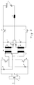
- the second variant of the circuit according to the invention for an arc welding device shown in FIG. 4 also shows a current transformer 15a, 15b fed by an intermediate circuit 2, the primary winding of which is fed by semiconductor switches 16, 17, 18, 19 arranged in a bridge circuit in such a way that alternating currents each occur result with changing sign, which flow into the primary winding 15a.
- the free-wheeling diodes 16a-19a are connected in parallel to the semiconductor switches 16-19.
- two current paths connected in parallel are provided, the components of which are provided with the corresponding reference numerals.
- decoupling diodes 19, 20 are also provided in FIG. 4, since both current paths are connected together to the single secondary winding 15b.
Abstract
Description
Die Erfindung betrifft ein Lichtbogenschweißgerät mit einem wechselstromgespeisten Gleichrichter, der einen Zwischenkreis speist, einem primärseitig getakteten Stromwandler, dem sekundärseitig zwei parallele Strompfade zugeordnet sind, von denen der Schweißprozeß zeitversetzt in entgegengesetzter Richtung beaufschlagbar ist, wobei jeder der beiden Strompfade eine Freilaufdiode, eine Gleichrichterdiode und einen steuerbaren Halbleiterschalter aufweist, dessen Schalttakt die Arbeitsfrequenz des Lichtbogenschweißgerätes im Wechselstrombetrieb festlegt.The invention relates to an arc welding device with an AC-fed rectifier, which feeds an intermediate circuit, a current transformer clocked on the primary side, to which two parallel current paths are assigned on the secondary side, of which the welding process can be acted on with a time delay in the opposite direction, each of the two current paths being a free-wheeling diode, a rectifier diode and has a controllable semiconductor switch, the switching cycle of which determines the working frequency of the arc welding device in AC operation.
Ein solches Schweißgerät ist aus der deutschen Patentschrift 38 03 447 bekannt. Dieses bekannte Schweißgerät ermöglicht eine Versorgung des Schweißprozesse sowohl mit Gleich- als auch mit Wechselstrom. Wechselstromschweißen ist bei besonderen Anwendungsfällen technologisch vorteilhafter, da zum Beispiel beim Aluminiumschweißen die während einer Schweißperiode in der einen Stromrichtung gebildete Oxidschicht durch den entgegengerichteten Strom der nachfolgenden Periode wieder aufgebrochen wird. Bei dem bekannten Schweißgerät ist zusätzlich ein mechanischer Umschalter vorgesehen, in dessen erster Stellung für Gleichstrombetrieb beide Strompfade gemeinsam den Schweißprozeß speisen und in dessen zweiter, den Wechselstrombetrieb bestimmenden Stellung der erste Halbleiterschalter den Strom des ersten Strompfades und der zweite Halbleiterschalter der Strom des zweiten Strompfades führt. Ein solcher mechanischer Umschalter weist aufgrund seiner endlichen Standzeit im Dauerbetrieb Nachteile auf.Such a welding device is known from German Patent 38 03 447. This known welding device enables the welding processes to be supplied with both DC and DC Alternating current. AC welding is technologically more advantageous in special applications because, for example, in aluminum welding, the oxide layer formed in one current direction during a welding period is broken up again by the opposite current in the following period. In the known welding device, a mechanical changeover switch is additionally provided, in the first position for DC operation, both current paths feed the welding process together and in the second position, which determines AC operation, the first semiconductor switch carries the current of the first current path and the second semiconductor switch carries the current of the second current path . Such a mechanical switch has drawbacks due to its finite service life in continuous operation.
Es ist darüber hinaus ein Lichtbogenschweißgerät bekannt, bei welchem im Sekundärkreis eine aus vier Halbleiterschaltern gebildete Brückenschaltung vorgesehen ist, wobei durch die entsprechende Ansteuerung der Halbleiterschalter sowohl ein Gleichstrom- als auch einen Wechselstrombetrieb ermöglicht wird. Diese Lösung weist den Nachteil auf, daß im Betrieb an jedem der vier Halbleiterschalter Verlustleistung entsteht.In addition, an arc welding device is known in which a bridge circuit formed from four semiconductor switches is provided in the secondary circuit, both direct current and alternating current operation being made possible by the corresponding control of the semiconductor switches. This solution has the disadvantage that power dissipation occurs at each of the four semiconductor switches during operation.
Ein Schweißgerät der eingangs genannten Art ist auch aus der DE-OS 40 11 461 bekannt. Bei diesem Schweißgerät sind zur Versorgung der beiden sekundärseitigen Strompfade stets mindestens zwei separate Stromwandler erforderlich, von denen jeweils immer nur einer in einer Phase leitend ist. Dies bedeutet, daß zur Erhaltung der Funktion dieser Schaltung immer stets zwei Wandler aufgewendet werden müssen.A welding device of the type mentioned is also known from DE-OS 40 11 461. This welding device always requires at least two separate current transformers to supply the two secondary-side current paths, of which only one is always conductive in one phase. This means that two converters must always be used to maintain the function of this circuit.
Demgegenüber liegt der Erfindung die Aufgabe zugrunde, ein Lichtbogenschweißgerät der eingangs genannten Art dahingehend weiterzuentwickeln, daß es einerseits schaltungstechnisch vereinfacht ist und andererseits hinsichtlich der Verlustleistung optimiert ist.In contrast, the invention has for its object to further develop an arc welding device of the type mentioned in such a way that on the one hand it is simplified in terms of circuitry and on the other hand it is optimized with regard to power loss.
Diese Aufgabe wird bei einem Lichtbogenschweißgerät der eingangs genannten Art in einer ersten Variante der Erfindung dadurch gelöst, daß jeder der beiden Strompfade von räumlich getrennten Sekundärwicklungen gespeist wird, die von einer gemeinsamen Primärwicklung beaufschlagt werden und daß in jedem der beiden sekundärseitigen Strompfade ein separat ansteuerbarer Halbleiterschalter vorgesehen ist, die in einer Mittelpunktschaltung miteinander verknüpft sind, wobei die Halbleiterschalter derart steuerbar sind, daß entweder nur einer der beiden Strompfade leitend ist (DC-Ausgang) oder die beiden Strompfade wechselweise leitend sind (AC-Ausgang).This object is achieved in an arc welding device of the type mentioned in a first variant of the invention in that each of the two current paths is fed by spatially separate secondary windings which are acted upon by a common primary winding and in that in each of the two secondary-side current paths a separately controllable semiconductor switch is provided, which are linked together in a center circuit, the semiconductor switches being controllable such that either only one of the two current paths is conductive (DC output) or the two current paths are alternately conductive (AC output).
Nach einer zweiten Variante der Erfindung wird diese Aufgabe dadurch gelöst, daß die beiden Strompfade an einer gemeinsamen Sekundärwicklung liegen, wobei die Primärwicklung von in Brückenschaltung liegenden Primärschaltern derart gespeist wird, daß wechselweise Sekundärspannungen entgegensetzbaren Vorzeichens anliegen und daß in jedem der beiden sekundärseitigen Strompfade ein separat ansteuerbarer Halbleiterschalter vorgesehen ist, die in einer Mittelpunktschaltung miteinander verknüpft sind, wobei die Halbleiterschalter derart steuerbar sind, daß entweder nur einer der beiden Strompfade leitend ist (DC-Ausgang) oder die beiden Strompfade wechselweise leitend sind (AC-Ausgang).According to a second variant of the invention, this object is achieved in that the two current paths are connected to a common secondary winding, the primary winding being fed by primary switches located in a bridge circuit in such a way that alternating secondary voltages are available and that a separate one is present in each of the two secondary-side current paths controllable semiconductor switches are provided which are linked together in a center circuit, the semiconductor switches being controllable in such a way that either only one of the two current paths is conductive (DC output) or the two current paths are alternately conductive (AC output).
Die Erfindung zeichnet sich dadurch aus, daß der schaltungstechnische Aufwand dadurch herabgesetzt werden kann, daß nunmehr nur noch ein Wandler erforderlich ist.The invention is characterized in that the circuit complexity can be reduced by the fact that now only one converter is required.
Durch die Anordnung und die Ansteuerung der Halbleiterschalter wird jeweils erreicht, daß stets nur eine der beiden Strompfade aktiviert ist und der andere entsprechend ausgeblendet wird. Dabei unterscheiden sich die beiden Varianten dadurch, daß gemäß der ersten Variante zwei von einer gemeinsamen Primärwicklung gespeiste separate Sekundärwicklungen vorgsehen sind, während gemäß der zweiten Variante eine gemeinsame Sekundärwickllung vorgesehen ist, die durch primärseitige Taktung entsprechend wechselweise entgegengesetzte Polarität erhält. Beiden Varianten ist gemeinsam, daß stets ein einziger Wandler ausreicht.The arrangement and the control of the semiconductor switches ensure that only one of the two current paths is always activated and the other is correspondingly hidden. The two variants differ in that, according to the first variant, two separate secondary windings fed by a common primary winding are provided, while according to the second variant a common secondary winding is provided, which receives alternately opposite polarity by clocking on the primary side. Both variants have in common that a single converter is always sufficient.
Die Erfindung zeichnet sich darüber hinaus dadurch aus, daß allein durch die Ansteuerung der sekundärseitigen Halbleiterschalter sowohl die Betriebsart (Gleichstrom oder Wechselstrom) an sich als auch in der Betriebsart "Wechselstrom" die Arbeitsfrequenz für die Versorgung des Schweißprozesses bestimmt werden können. Zusätzliche Schaltungsmittel, wie ein mechanischer Umschalter, können daher entfallen. In der Betriebsart "Gleichstrom" ist alternativ nur einer der beiden Halbleiterschalter ständig leitend und der andere ständig gesperrt. Hierdurch enststeht nur in dem den leitenden Halbleiterschalter enthaltenden Strompfad Verlustsleistung, während der andere Strompfad keine Verluste erzeugt. Im Wechselstrombetriebszustand sind die Halbleiterschalter wechselweise mit der Arbeitsfrequenz getaktet leitend, wobei während der leitenden Phase des einen Schalters der den anderen Schalter enthaltende Strompfad wiederum keine Verlustleistung hervorruft und umgekehrt. Gegenüber den bekannten Lösungen ergibt sich somit einerseits eine Reduzierung der erforderlichen Schaltelemente und andererseits gegenüber der bekannten Lösung mit der Brückenschaltung eine Reduzierung der Verluste auf den halben Wert.The invention is further characterized in that both the operating mode (direct current or alternating current) itself and in the "alternating current" operating mode, the working frequency for the supply of the welding process can be determined solely by controlling the secondary-side semiconductor switches. Additional switching means, such as a mechanical switch, can therefore be omitted. In the "direct current" operating mode, alternatively only one of the two semiconductor switches is continuously conductive and the other is permanently blocked. This results in loss power only in the current path containing the conductive semiconductor switch, while the other current path generates no losses. In the AC operating state, the semiconductor switches are alternately conductive, clocked at the operating frequency, with the current path containing the other switch in turn causing no power loss during the conductive phase of the one switch, and vice versa. Compared to the known solutions, this results on the one hand in a reduction in the required switching elements and, on the other hand, in comparison with the known solution with the bridge circuit, a reduction in losses to half the value.
Die zweite Variante hat den weiteren Vorteil, daß gegenüber der ersten Variante mindestens eine Wicklung gespart werden kann. Auch hierdurch wird der schaltungstechnische Aufwand weiter herabgesetzt. Hinsichtlich des praktischen Schaltungsaufbaus ergibt sich bei der ersten Variante der Erfindung der Vorteil, daß Freilaufdioden, Gleichrichterdioden und sekundärseite Halbleiterschalter auf einem gemeinsamen Kühlkörper angeordnet sein können. Gegenüber der bekannten Lösung kann hierbei ein Kühlkörper eingespart werden.The second variant has the further advantage that at least one winding can be saved compared to the first variant. This also further reduces the complexity of the circuitry. With regard to the practical circuit structure, the advantage of the first variant of the invention is that free-wheeling diodes, rectifier diodes and secondary-side semiconductor switches can be arranged on a common heat sink. Compared to the known solution, a heat sink can be saved here.
Vorzugsweise sind die Strompfade wechselweise über sich nicht überlappende Zeitintervalle leitend.The current paths are preferably conductive alternately over non-overlapping time intervals.
Bei der ersten Variante kann es ferner vorteilhaft sein, daß die Primärwicklung zur Speisung der beiden räumlich getrennten Sekundärwicklungen ebenfalls in zwei Teilwicklungen aufgeteilt ist, die von zwei in Reihe zu ihr liegende gemeinsam getaktete Primärschalter gespeist sind.In the first variant, it can also be advantageous that the primary winding for feeding the two spatially separate secondary windings is also divided into two partial windings, which are fed by two clocked primary switches lying in series with it.
Die erfindungsgemäße Lösung läßt sich nicht nur auf die sogenannten Inverterstromquellen anwenden sondern auch auf herkömmliche Stromquellen mit einer Arbeitsfrequenz von 50 Hz, die aus einem Netztransformator und einem herkömmlichen Dreiphasengleichrichter bestehen.The solution according to the invention can be applied not only to the so-called inverter current sources, but also to conventional current sources with an operating frequency of 50 Hz, which consist of a mains transformer and a conventional three-phase rectifier.
Die Erfindung wird im folgenden anhand einer Zeichnung näher erläutert:
Dabei zeigen:
- Fig. 1
- ein erstes Ausführungsbeispiel der ersten Variante einer Schaltung für das erfindungsgemäße Lichtbogenschweißgerät,
- Fig. 2
- ein zweites Ausführungsbeispiel der ersten Variante,
- Fig. 3
- ein drittes Ausführungsbeispiel der ersten Variante und
- Fig. 4
- ein Ausführungsbeispiel der zweiten Variante einer Schaltung für das erfindungsgemäße Lichtbogenschweißgerät.
Show:
- Fig. 1
- a first embodiment of the first variant of a circuit for the arc welding device according to the invention,
- Fig. 2
- a second embodiment of the first variant,
- Fig. 3
- a third embodiment of the first variant and
- Fig. 4
- an embodiment of the second variant of a circuit for the arc welding device according to the invention.
Fig. 1 zeigt einen von einem Ein- oder Dreiphasennetz gespeisten Gleichrichter 1, der sowohl mit gesteuerten als auch mit ungesteuerten Stromventilen ausgerüstet sein kann. Der Gleichrichter 1 speist einen einen Zwischenkreis bildenden Kondensator 2, der seinerseits den ihm nachgeordneten Stromwandler 5a,5b,5c versorgt. Die Primärwicklung 5a des Stromwandlers wird von Primärhalbleiterschaltern 4a,4b getaktet angesteuert. Zusätzlich sind Freilaufdioden 3a,3b vorgesehen, die eine Abmagnetisierung des Stromwandlers 5a,5b,5c während derjenigen Zeitintervalle bewirken, in denen der Wandler nicht durch die Halbleiterschalter 4a,4b getaktet wird. Die Sekundärseite des Stromwandlers wird durch zwei getrennte Sekundärwicklungen 5b,5c gebildet, deren Wicklungssinn gleich ist, wie die durch die entsprechenden Punkte dargestellt ist. An die obere Sekundärwicklung 5b ist ein erster Strompfad angeschlossen, welcher aus den Bauelementen Gleichrichterdiode 6, gesteuertem Halbleiterschalter 10, Schweißprozeß 13, Glättungsdrossel 12 und Freilaufdiode 7 besteht.Fig. 1 shows a
An der unteren Sekundärwicklung 5c ist ein zweiter Strompfad angeschlossen, der aus den Elementen Gleichrichterdiode 8, Glättungsdrossel 12, Schweißprozeß 13, gesteuerten Halbleiterschalter 11 und Freilaufdiode 9 besteht.A second current path is connected to the lower
Die beiden Strompfade sind so geschaltet, daß bei Beaufschlagung des oberen Strompfades der Schweißprozeß 13 in einer ersten Stromrichtung und bei Beaufschlagung des unteren Strompfades in der entgegengesetzten, zweiten Stromrichtung durchflossen wird.The two current paths are switched such that the
Die Arbeitsweise der erfindungsgemäßen Schaltung für das Lichtbogenschweißgerät gemäß Fig.1 ist nun wie folgt:
Der Stromwandler 5a,5b,5c arbeitet durch die Taktung der primärseiten Halbleiterschalter 4a,4b mit einer Taktfrequenz von etwa 20 kHz. Die Sekundärspannungen werden über die Gleichrichterdioden 6 bzw. 8 gleichgerichtet, so daß an deren Ausgang zwei Gleichspannungen für jeden der beiden Strompfade zur Verfügung stehen. Soll das Lichtbogenschweißgerät mit Gleichstrom gespeist werden, so ist nur eine der beiden sekundärseitigen Halbleiterschalter 10,11 leitend, während der andere dauernd gesperrt ist. Wenn dies beispielsweise der Schalter 10 ist, fließt nur Strom durch den Schweißprozeß in der ersten Richtung. In dem jeweils nicht aktivierten Strompfad kann in diesem Betriebszustand keine Verlustleistung entstehen.The method of operation of the circuit according to the invention for the arc welding device according to FIG. 1 is now as follows:
The
Wenn die Betriebsart Wechselstrom gewünscht ist, werden die sekundärseitigen Halbleiterschalter 10,11 von einer nicht näher dargestellten Steuereinrichtung derart getaktet, daß sie wechselweise leitend sind. Die Taktung erfolgt in der gewünschten Betriebsfrequenz für den Schweißprozeß, beispielsweise 200 Hz. Da diese Frequenz wesentlich niedriger ist als die Taktfrequenz des Stromwandlers, wird die jeweils an den Gleichrichterdioden 6 bzw. 8 zur Verfügung stehende Gleichspannung nahezu unverformt an den Schweißprozeß übertragen. Somit ergibt sich eine nahezu rechteckförmige Arbeitsspannung am Schweißprozeß, die der Frequenz der Taktfrequenz der Halbleiterschalter 10,11 entspricht.If the alternating current operating mode is desired, the secondary-
Das in Fig. 2 dargestellte Ausführungsbeispiel unterscheidet sich von dem in Fig. 1 dargestellten nur dadurch, daß die in Mittelpunktsschaltung angeordneten sekundärseitigen Halbleiterschalter 10,11 im Verbindungszweig zwischen der Glättungsdrossel 12 und den jeweiligen Gleichrichterdioden 6,8 angeordnet sind. Diese räumliche Schaltungsanordnung hat den Vorteil, daß Gleichrichterdioden 6,8, Freilaufdioden 7,9 und sekundärseitige Halbleiterschalter 10,11 auf einem einzigen Kühlkörper angeordnet sein können, wobei die zum oberen Strompfad gehörigen Elemente miteinander verbunden und gegenüber den zum unteren Strompfad gehörigen Elementen isoliert sind, die ihrerseits miteinander verbunden sind.The embodiment shown in FIG. 2 differs from that shown in FIG. 1 only in that the secondary semiconductor switches 10, 11 arranged in the center circuit are arranged in the connecting branch between the smoothing
Das in Fig. 3 dargestellte Ausführungsbeispiel unterscheidet sich von den zuvor dargestellten Ausführungsbeispielen dadurch, daß die Primärwicklung durch zwei getrennte Teilwicklungen 5a,14a gebildet ist. Die beiden Teilwicklungen sind parallel zueinander geschaltet und weisen jeweils den entsprechenden Wicklungssinn auf.The exemplary embodiment shown in FIG. 3 differs from the previously illustrated exemplary embodiments in that the primary winding is formed by two separate
Die in Fig. 4 dargestellte zweite Variante der erfindungsgemäßen Schaltung für ein Lichtbogenschweißgerät zeigt ebenso einen von einem Zwischenkreis 2 gespeisten Stromwandler 15a,15b, dessen Primärwicklung von in Brückenschaltung angeordneten Halberleiterschaltern 16,17,18,19 derart gespeist wird, daß sich wechselweise Ströme jeweils mit wechselndem Vorzeichen ergeben, die in die Primärwicklung 15a fließen. Den Halbleiterschaltern 16 - 19 sind jeweils Freilaufdioden 16a - 19a parallel geschaltet. Sekundärseitig sind ebenso wie bei der ersten erfindungsgemäßen Variante zwei parallel geschaltete Strompfade vorgesehen, deren Bauelemente mit den entsprechenden Bezugszeichen versehen sind. Zusätzlich sind in Fig.4 noch Entkopplungsdioden 19,20 vorgesehen, da beide Strompfade gemeinsam an der einzigen Sekundärwicklung 15b angeschlossen sind.The second variant of the circuit according to the invention for an arc welding device shown in FIG. 4 also shows a
Im Unterschied zur ersten Variante, bei der an den Wicklungen 5b,5c bzw. 5b,14b auf der Sekundärseite jeweils gleichzeitig die induzierten Spannungen für die beiden Strompfade vorhanden sind, ist beim Ausführungsbeispiel nach Fig.4 jeweils zeitversetzt eine induzierte Spannung mit positiver bzw. negativer Vorzeichenorientierung vorhanden, mit denen die beiden Strompfade gespeist werden, wobei während der einen (positiven) Halbwelle des Schweißstromes die Halbleiterschalter 17,19 leitend sind und während der anderen (negativen) Halbwelle die Halbleiterschalter 16,18.In contrast to the first variant, in which the induced voltages for the two current paths are present simultaneously on the
Claims (7)
- An arc welding apparatus with an a.c.-powered rectifier (1) which powers an intermediate circuit (2), a current transformer (5, 14, 15) which is cycled on the primary side and to which two parallel current paths are associated on the secondary side, by means of which the welding process (13) is powerable in the opposite direction in a time-displaced manner, with each of the two current paths comprising a freewheeling diode (7, 9), a rectifier diode (6, 8) and a controllable semiconductor switch whose switching cycle determines the working frequency of the arc welding apparatus in a.c. operation, characterized in that each of the two current paths is powered by spatially separated secondary windings (5b, 5c) which are charged by a common primary winding and that in each of the two current paths on the secondary side there is provided a separately controllable semiconductor switch (10, 11), which switches are mutually linked in a centre tap connection, with the semiconductor switches (10, 11) being controllable in such a way that either only one of the two current paths is conductive (DC output) or both current paths are alternatingly conductive (AC output).
- An arc welding apparatus with an a.c.-powered rectifier (1) which powers an intermediate circuit (2), a current transformer (5, 14, 15) which is cycled on the primary side and to which two parallel current paths are associated on the secondary side, by means of which the welding process (13) is chargeable in the opposite direction in a time-displaced manner, with each of the two current paths comprising a freewheeling diode (7, 9), a rectifier diode (6, 8) and a controllable semiconductor switch whose switching cycle determines the working frequency of the arc welding apparatus in a.c. operation, characterized in that the two current paths are disposed in a common secondary winding, with the primary winding (15a) being powered by the primary switches (16 to 19) disposed in a bridge circuit in such a way that alternating secondary voltages of opposable signs are applied and that in each of the two current paths on the secondary side there is provided a separately controllable semiconductor switch (10, 11), which switches are mutually linked in a centre tap connection, with the semiconductor switches (10, 11) being controllable in such a way that either only one of the two current paths is conductive (DC output) or both current paths are alternatingly conductive (AC output).
- An arc welding apparatus as claimed in claim 1, characterized in that the current paths are alternatingly conductive over non-overlapping time intervals.
- An arc welding apparatus as claimed in claim 3, characterized in that the primary winding (5a) is powered by two jointly cycled primary switches (4a, 4b) being in series thereto.
- An arc welding apparatus as claimed in claim 3 or 4, characterized in that the primary winding comprises two partial windings (5a, 14a) which are associated with the respective secondary winding.
- An arc welding apparatus as claimed in claim 1, 3, 4 or 5, characterized in that the freewheeling diodes (7, 9) on the secondary side, the rectifier diodes (6, 8) on the secondary side and the semiconductor switches (10, 11) on the secondary side are arranged on a common heat sink.
- An arc welding apparatus as claimed in one of the preceding claims, characterized in that the inverter current source consisting of rectifier (1), intermediate circuit (2) and current transformer (5, 14, 15) is replaced by a current source consisting of a power transformer and a three-phase rectifier.
Applications Claiming Priority (2)
| Application Number | Priority Date | Filing Date | Title |
|---|---|---|---|
| DE4302443 | 1993-01-29 | ||
| DE4302443A DE4302443C1 (en) | 1993-01-29 | 1993-01-29 | Arc welding equipment with semiconductor-switched sec. current paths - is based on switched-prim. transformer with two sec. windings in same direction switched by separate semiconductors in push=pull mode |
Publications (2)
| Publication Number | Publication Date |
|---|---|
| EP0608536A1 EP0608536A1 (en) | 1994-08-03 |
| EP0608536B1 true EP0608536B1 (en) | 1996-01-31 |
Family
ID=6479168
Family Applications (1)
| Application Number | Title | Priority Date | Filing Date |
|---|---|---|---|
| EP93120107A Expired - Lifetime EP0608536B1 (en) | 1993-01-29 | 1993-12-14 | Arc welding apparatus with semiconducting switches having a central connexion |
Country Status (3)
| Country | Link |
|---|---|
| EP (1) | EP0608536B1 (en) |
| AT (1) | ATE133596T1 (en) |
| DE (2) | DE4302443C1 (en) |
Cited By (2)
| Publication number | Priority date | Publication date | Assignee | Title |
|---|---|---|---|---|
| US6115273A (en) * | 1998-07-09 | 2000-09-05 | Illinois Tool Works Inc. | Power converter with low loss switching |
| US6865096B1 (en) | 1998-07-09 | 2005-03-08 | Illinois Tool Works Inc. | Power convertor with low loss switching |
Families Citing this family (5)
| Publication number | Priority date | Publication date | Assignee | Title |
|---|---|---|---|---|
| DE19517875C2 (en) * | 1995-05-16 | 1997-05-07 | Michael Szczesny | Arc welding machine with improved dynamics |
| JP2980827B2 (en) * | 1995-06-23 | 1999-11-22 | 株式会社三社電機製作所 | Arc welding machine |
| AT406807B (en) * | 1996-09-27 | 2000-09-25 | Fronius Schweissmasch | Power section and secondary section for a transformer |
| DE19738453C2 (en) * | 1997-09-03 | 2002-10-31 | Wolfgang Schuster | Inverter power source |
| SI25535A (en) * | 2017-10-26 | 2019-04-30 | Univerza v Mariboru, Fakulteta za elektrotehniko, računalništvo in informatiko | A welding transformator |
Family Cites Families (5)
| Publication number | Priority date | Publication date | Assignee | Title |
|---|---|---|---|---|
| DE2913625A1 (en) * | 1979-04-05 | 1980-10-16 | Messer Griesheim Gmbh | DEVICE FOR DC AND / OR AC ARC WELDING WITH A INVERTER TO BE CONNECTED TO AN AC OR DC NETWORK |
| DE3803447C1 (en) * | 1988-02-05 | 1989-05-24 | B & V Beschichten Und Verbinden Gmbh, 6800 Mannheim, De | |
| DE3806983C2 (en) * | 1988-03-03 | 1994-07-21 | Siemens Ag | Circuit arrangement for generating voltages of different polarities |
| DE4011461A1 (en) * | 1989-07-26 | 1991-01-31 | Ehrhard Prof Dipl I Futterlieb | Electrical supply control for electric arc welding unit - avoids use of mechanical switch in signal circuit and has switch to select direct or alternating current supply |
| DE4128175C2 (en) * | 1991-08-24 | 1994-05-19 | Elektro Werk Muendersbach Gmbh | Arc welder |
-
1993
- 1993-01-29 DE DE4302443A patent/DE4302443C1/en not_active Expired - Fee Related
- 1993-12-14 AT AT93120107T patent/ATE133596T1/en not_active IP Right Cessation
- 1993-12-14 DE DE59301559T patent/DE59301559D1/en not_active Expired - Lifetime
- 1993-12-14 EP EP93120107A patent/EP0608536B1/en not_active Expired - Lifetime
Cited By (4)
| Publication number | Priority date | Publication date | Assignee | Title |
|---|---|---|---|---|
| US6115273A (en) * | 1998-07-09 | 2000-09-05 | Illinois Tool Works Inc. | Power converter with low loss switching |
| US6865096B1 (en) | 1998-07-09 | 2005-03-08 | Illinois Tool Works Inc. | Power convertor with low loss switching |
| US7336512B2 (en) | 1998-07-09 | 2008-02-26 | Illinois Tool Works Inc. | Power convertor with low loss switching |
| US7778056B2 (en) | 1998-07-09 | 2010-08-17 | Geissler Steven J | Power converter with low loss switching |
Also Published As
| Publication number | Publication date |
|---|---|
| DE59301559D1 (en) | 1996-03-14 |
| ATE133596T1 (en) | 1996-02-15 |
| DE4302443C1 (en) | 1994-05-26 |
| EP0608536A1 (en) | 1994-08-03 |
Similar Documents
| Publication | Publication Date | Title |
|---|---|---|
| DE3034693C2 (en) | Pulse-width controlled push-pull DC voltage converter | |
| EP0231481B1 (en) | Ac-dc converter provided with an asymmetric half-bridge circuit | |
| EP0283842B1 (en) | Flyback switching converter | |
| DE3109073A1 (en) | POWER SUPPLY DEVICE | |
| EP0396126A2 (en) | Power supply device | |
| DE3912849C2 (en) | ||
| EP0608536B1 (en) | Arc welding apparatus with semiconducting switches having a central connexion | |
| EP1085646B1 (en) | DC/DC converter | |
| DE10238606B4 (en) | Switching Power Supply | |
| WO2011047818A1 (en) | Device for controlling a plurality of electrical consumers | |
| EP0265938B1 (en) | DC-DC converter | |
| DE2554826A1 (en) | TRANSFER ARRANGEMENT FOR A CURRENT CONVERTER CIRCUIT | |
| DE4128175A1 (en) | Arc welding appts. - has main voltage-fed DC rectifier, intermediate circuit prim. side transformer, sec. side transformer and AC rectifier, etc. | |
| DE4342327C2 (en) | Switching power supply supported by a battery | |
| EP0743126B1 (en) | Arc welding device with improved dynamic characteristics | |
| EP0326681B1 (en) | Arc welding apparatus for direct and alternating current supply | |
| DE2819676A1 (en) | DC voltage converter for power supply - has at least two half-bridge converters using transformer primary winding sections separated by transistors | |
| EP0410088A2 (en) | Welding or plasma cutting device with stabilized voltage of indirect circuit | |
| DE4411227A1 (en) | Arc welding appts. with resonance switching circuit | |
| EP0792538A1 (en) | Circuit for the multiple use of a transformer core | |
| EP0833430B1 (en) | Power stage and secondary stage for a transformer | |
| DE3241821C2 (en) | ||
| DE3049020C2 (en) | Controllable DC / DC converter for power switch-mode power supplies | |
| DE2849575C2 (en) | Clocked power supply | |
| EP0263936A1 (en) | Secondary side switchable power supply device |
Legal Events
| Date | Code | Title | Description |
|---|---|---|---|
| PUAI | Public reference made under article 153(3) epc to a published international application that has entered the european phase |
Free format text: ORIGINAL CODE: 0009012 |
|
| AK | Designated contracting states |
Kind code of ref document: A1 Designated state(s): AT BE CH DE DK ES FR GB GR IE IT LI LU MC NL PT SE |
|
| 17P | Request for examination filed |
Effective date: 19940712 |
|
| 17Q | First examination report despatched |
Effective date: 19941130 |
|
| GRAA | (expected) grant |
Free format text: ORIGINAL CODE: 0009210 |
|
| AK | Designated contracting states |
Kind code of ref document: B1 Designated state(s): AT BE CH DE DK ES FR GB GR IE IT LI LU MC NL PT SE |
|
| PG25 | Lapsed in a contracting state [announced via postgrant information from national office to epo] |
Ref country code: NL Free format text: LAPSE BECAUSE OF FAILURE TO SUBMIT A TRANSLATION OF THE DESCRIPTION OR TO PAY THE FEE WITHIN THE PRESCRIBED TIME-LIMIT Effective date: 19960131 Ref country code: GR Free format text: LAPSE BECAUSE OF FAILURE TO SUBMIT A TRANSLATION OF THE DESCRIPTION OR TO PAY THE FEE WITHIN THE PRESCRIBED TIME-LIMIT Effective date: 19960131 Ref country code: ES Free format text: THE PATENT HAS BEEN ANNULLED BY A DECISION OF A NATIONAL AUTHORITY Effective date: 19960131 Ref country code: DK Effective date: 19960131 Ref country code: BE Effective date: 19960131 |
|
| REF | Corresponds to: |
Ref document number: 133596 Country of ref document: AT Date of ref document: 19960215 Kind code of ref document: T |
|
| REG | Reference to a national code |
Ref country code: IE Ref legal event code: FG4D Free format text: 67112 |
|
| REF | Corresponds to: |
Ref document number: 59301559 Country of ref document: DE Date of ref document: 19960314 |
|
| GBT | Gb: translation of ep patent filed (gb section 77(6)(a)/1977) |
Effective date: 19960221 |
|
| ITF | It: translation for a ep patent filed |
Owner name: SOCIETA' ITALIANA BREVETTI S.P.A. |
|
| PG25 | Lapsed in a contracting state [announced via postgrant information from national office to epo] |
Ref country code: SE Effective date: 19960430 Ref country code: PT Effective date: 19960430 |
|
| ET | Fr: translation filed | ||
| NLV1 | Nl: lapsed or annulled due to failure to fulfill the requirements of art. 29p and 29m of the patents act | ||
| PG25 | Lapsed in a contracting state [announced via postgrant information from national office to epo] |
Ref country code: IE Free format text: LAPSE BECAUSE OF NON-PAYMENT OF DUE FEES Effective date: 19960814 |
|
| REG | Reference to a national code |
Ref country code: IE Ref legal event code: FD4D Ref document number: 67112 Country of ref document: IE |
|
| PLBE | No opposition filed within time limit |
Free format text: ORIGINAL CODE: 0009261 |
|
| STAA | Information on the status of an ep patent application or granted ep patent |
Free format text: STATUS: NO OPPOSITION FILED WITHIN TIME LIMIT |
|
| PG25 | Lapsed in a contracting state [announced via postgrant information from national office to epo] |
Ref country code: AT Effective date: 19961214 |
|
| PG25 | Lapsed in a contracting state [announced via postgrant information from national office to epo] |
Ref country code: LU Free format text: LAPSE BECAUSE OF NON-PAYMENT OF DUE FEES Effective date: 19961231 Ref country code: LI Effective date: 19961231 Ref country code: CH Effective date: 19961231 |
|
| 26N | No opposition filed | ||
| PG25 | Lapsed in a contracting state [announced via postgrant information from national office to epo] |
Ref country code: MC Effective date: 19970630 |
|
| REG | Reference to a national code |
Ref country code: CH Ref legal event code: PL |
|
| REG | Reference to a national code |
Ref country code: GB Ref legal event code: 711L |
|
| PG25 | Lapsed in a contracting state [announced via postgrant information from national office to epo] |
Ref country code: FR Free format text: LAPSE BECAUSE OF NON-PAYMENT OF DUE FEES Effective date: 20010831 |
|
| REG | Reference to a national code |
Ref country code: FR Ref legal event code: ST Ref country code: FR Ref legal event code: CD |
|
| REG | Reference to a national code |
Ref country code: GB Ref legal event code: 711G |
|
| REG | Reference to a national code |
Ref country code: FR Ref legal event code: D3 |
|
| REG | Reference to a national code |
Ref country code: GB Ref legal event code: IF02 |
|
| PGFP | Annual fee paid to national office [announced via postgrant information from national office to epo] |
Ref country code: GB Payment date: 20021209 Year of fee payment: 10 Ref country code: FR Payment date: 20021209 Year of fee payment: 10 |
|
| PG25 | Lapsed in a contracting state [announced via postgrant information from national office to epo] |
Ref country code: GB Free format text: LAPSE BECAUSE OF NON-PAYMENT OF DUE FEES Effective date: 20031214 |
|
| GBPC | Gb: european patent ceased through non-payment of renewal fee |
Effective date: 20031214 |
|
| REG | Reference to a national code |
Ref country code: FR Ref legal event code: ST |
|
| PG25 | Lapsed in a contracting state [announced via postgrant information from national office to epo] |
Ref country code: IT Free format text: LAPSE BECAUSE OF NON-PAYMENT OF DUE FEES;WARNING: LAPSES OF ITALIAN PATENTS WITH EFFECTIVE DATE BEFORE 2007 MAY HAVE OCCURRED AT ANY TIME BEFORE 2007. THE CORRECT EFFECTIVE DATE MAY BE DIFFERENT FROM THE ONE RECORDED. Effective date: 20051214 |
|
| PGFP | Annual fee paid to national office [announced via postgrant information from national office to epo] |
Ref country code: DE Payment date: 20091222 Year of fee payment: 17 |
|
| REG | Reference to a national code |
Ref country code: DE Ref legal event code: R119 Ref document number: 59301559 Country of ref document: DE Effective date: 20110701 |
|
| PG25 | Lapsed in a contracting state [announced via postgrant information from national office to epo] |
Ref country code: DE Free format text: LAPSE BECAUSE OF NON-PAYMENT OF DUE FEES Effective date: 20110701 |