EP0608440A1 - Semiconductor device having a plurality of chips having identical circuit arrangements sealed in package - Google Patents
Semiconductor device having a plurality of chips having identical circuit arrangements sealed in package Download PDFInfo
- Publication number
- EP0608440A1 EP0608440A1 EP92121643A EP92121643A EP0608440A1 EP 0608440 A1 EP0608440 A1 EP 0608440A1 EP 92121643 A EP92121643 A EP 92121643A EP 92121643 A EP92121643 A EP 92121643A EP 0608440 A1 EP0608440 A1 EP 0608440A1
- Authority
- EP
- European Patent Office
- Prior art keywords
- chips
- chip
- main surface
- semiconductor device
- terminals
- Prior art date
- Legal status (The legal status is an assumption and is not a legal conclusion. Google has not performed a legal analysis and makes no representation as to the accuracy of the status listed.)
- Ceased
Links
Images


Classifications
-
- H—ELECTRICITY
- H01—ELECTRIC ELEMENTS
- H01L—SEMICONDUCTOR DEVICES NOT COVERED BY CLASS H10
- H01L24/00—Arrangements for connecting or disconnecting semiconductor or solid-state bodies; Methods or apparatus related thereto
- H01L24/01—Means for bonding being attached to, or being formed on, the surface to be connected, e.g. chip-to-package, die-attach, "first-level" interconnects; Manufacturing methods related thereto
- H01L24/02—Bonding areas ; Manufacturing methods related thereto
- H01L24/04—Structure, shape, material or disposition of the bonding areas prior to the connecting process
- H01L24/06—Structure, shape, material or disposition of the bonding areas prior to the connecting process of a plurality of bonding areas
-
- H—ELECTRICITY
- H01—ELECTRIC ELEMENTS
- H01L—SEMICONDUCTOR DEVICES NOT COVERED BY CLASS H10
- H01L23/00—Details of semiconductor or other solid state devices
- H01L23/48—Arrangements for conducting electric current to or from the solid state body in operation, e.g. leads, terminal arrangements ; Selection of materials therefor
- H01L23/488—Arrangements for conducting electric current to or from the solid state body in operation, e.g. leads, terminal arrangements ; Selection of materials therefor consisting of soldered or bonded constructions
- H01L23/495—Lead-frames or other flat leads
- H01L23/49503—Lead-frames or other flat leads characterised by the die pad
- H01L23/4951—Chip-on-leads or leads-on-chip techniques, i.e. inner lead fingers being used as die pad
-
- H—ELECTRICITY
- H01—ELECTRIC ELEMENTS
- H01L—SEMICONDUCTOR DEVICES NOT COVERED BY CLASS H10
- H01L23/00—Details of semiconductor or other solid state devices
- H01L23/48—Arrangements for conducting electric current to or from the solid state body in operation, e.g. leads, terminal arrangements ; Selection of materials therefor
- H01L23/488—Arrangements for conducting electric current to or from the solid state body in operation, e.g. leads, terminal arrangements ; Selection of materials therefor consisting of soldered or bonded constructions
- H01L23/495—Lead-frames or other flat leads
- H01L23/49575—Assemblies of semiconductor devices on lead frames
-
- H—ELECTRICITY
- H01—ELECTRIC ELEMENTS
- H01L—SEMICONDUCTOR DEVICES NOT COVERED BY CLASS H10
- H01L24/00—Arrangements for connecting or disconnecting semiconductor or solid-state bodies; Methods or apparatus related thereto
- H01L24/01—Means for bonding being attached to, or being formed on, the surface to be connected, e.g. chip-to-package, die-attach, "first-level" interconnects; Manufacturing methods related thereto
- H01L24/42—Wire connectors; Manufacturing methods related thereto
- H01L24/47—Structure, shape, material or disposition of the wire connectors after the connecting process
- H01L24/48—Structure, shape, material or disposition of the wire connectors after the connecting process of an individual wire connector
-
- H—ELECTRICITY
- H01—ELECTRIC ELEMENTS
- H01L—SEMICONDUCTOR DEVICES NOT COVERED BY CLASS H10
- H01L25/00—Assemblies consisting of a plurality of individual semiconductor or other solid state devices ; Multistep manufacturing processes thereof
- H01L25/03—Assemblies consisting of a plurality of individual semiconductor or other solid state devices ; Multistep manufacturing processes thereof all the devices being of a type provided for in the same subgroup of groups H01L27/00 - H01L33/00, or in a single subclass of H10K, H10N, e.g. assemblies of rectifier diodes
- H01L25/04—Assemblies consisting of a plurality of individual semiconductor or other solid state devices ; Multistep manufacturing processes thereof all the devices being of a type provided for in the same subgroup of groups H01L27/00 - H01L33/00, or in a single subclass of H10K, H10N, e.g. assemblies of rectifier diodes the devices not having separate containers
- H01L25/065—Assemblies consisting of a plurality of individual semiconductor or other solid state devices ; Multistep manufacturing processes thereof all the devices being of a type provided for in the same subgroup of groups H01L27/00 - H01L33/00, or in a single subclass of H10K, H10N, e.g. assemblies of rectifier diodes the devices not having separate containers the devices being of a type provided for in group H01L27/00
- H01L25/0652—Assemblies consisting of a plurality of individual semiconductor or other solid state devices ; Multistep manufacturing processes thereof all the devices being of a type provided for in the same subgroup of groups H01L27/00 - H01L33/00, or in a single subclass of H10K, H10N, e.g. assemblies of rectifier diodes the devices not having separate containers the devices being of a type provided for in group H01L27/00 the devices being arranged next and on each other, i.e. mixed assemblies
-
- H—ELECTRICITY
- H01—ELECTRIC ELEMENTS
- H01L—SEMICONDUCTOR DEVICES NOT COVERED BY CLASS H10
- H01L2224/00—Indexing scheme for arrangements for connecting or disconnecting semiconductor or solid-state bodies and methods related thereto as covered by H01L24/00
- H01L2224/01—Means for bonding being attached to, or being formed on, the surface to be connected, e.g. chip-to-package, die-attach, "first-level" interconnects; Manufacturing methods related thereto
- H01L2224/02—Bonding areas; Manufacturing methods related thereto
- H01L2224/04—Structure, shape, material or disposition of the bonding areas prior to the connecting process
- H01L2224/0401—Bonding areas specifically adapted for bump connectors, e.g. under bump metallisation [UBM]
-
- H—ELECTRICITY
- H01—ELECTRIC ELEMENTS
- H01L—SEMICONDUCTOR DEVICES NOT COVERED BY CLASS H10
- H01L2224/00—Indexing scheme for arrangements for connecting or disconnecting semiconductor or solid-state bodies and methods related thereto as covered by H01L24/00
- H01L2224/01—Means for bonding being attached to, or being formed on, the surface to be connected, e.g. chip-to-package, die-attach, "first-level" interconnects; Manufacturing methods related thereto
- H01L2224/02—Bonding areas; Manufacturing methods related thereto
- H01L2224/04—Structure, shape, material or disposition of the bonding areas prior to the connecting process
- H01L2224/04042—Bonding areas specifically adapted for wire connectors, e.g. wirebond pads
-
- H—ELECTRICITY
- H01—ELECTRIC ELEMENTS
- H01L—SEMICONDUCTOR DEVICES NOT COVERED BY CLASS H10
- H01L2224/00—Indexing scheme for arrangements for connecting or disconnecting semiconductor or solid-state bodies and methods related thereto as covered by H01L24/00
- H01L2224/01—Means for bonding being attached to, or being formed on, the surface to be connected, e.g. chip-to-package, die-attach, "first-level" interconnects; Manufacturing methods related thereto
- H01L2224/02—Bonding areas; Manufacturing methods related thereto
- H01L2224/04—Structure, shape, material or disposition of the bonding areas prior to the connecting process
- H01L2224/05—Structure, shape, material or disposition of the bonding areas prior to the connecting process of an individual bonding area
- H01L2224/0554—External layer
- H01L2224/05599—Material
-
- H—ELECTRICITY
- H01—ELECTRIC ELEMENTS
- H01L—SEMICONDUCTOR DEVICES NOT COVERED BY CLASS H10
- H01L2224/00—Indexing scheme for arrangements for connecting or disconnecting semiconductor or solid-state bodies and methods related thereto as covered by H01L24/00
- H01L2224/01—Means for bonding being attached to, or being formed on, the surface to be connected, e.g. chip-to-package, die-attach, "first-level" interconnects; Manufacturing methods related thereto
- H01L2224/02—Bonding areas; Manufacturing methods related thereto
- H01L2224/04—Structure, shape, material or disposition of the bonding areas prior to the connecting process
- H01L2224/06—Structure, shape, material or disposition of the bonding areas prior to the connecting process of a plurality of bonding areas
- H01L2224/061—Disposition
- H01L2224/0612—Layout
- H01L2224/0613—Square or rectangular array
- H01L2224/06134—Square or rectangular array covering only portions of the surface to be connected
- H01L2224/06136—Covering only the central area of the surface to be connected, i.e. central arrangements
-
- H—ELECTRICITY
- H01—ELECTRIC ELEMENTS
- H01L—SEMICONDUCTOR DEVICES NOT COVERED BY CLASS H10
- H01L2224/00—Indexing scheme for arrangements for connecting or disconnecting semiconductor or solid-state bodies and methods related thereto as covered by H01L24/00
- H01L2224/01—Means for bonding being attached to, or being formed on, the surface to be connected, e.g. chip-to-package, die-attach, "first-level" interconnects; Manufacturing methods related thereto
- H01L2224/42—Wire connectors; Manufacturing methods related thereto
- H01L2224/47—Structure, shape, material or disposition of the wire connectors after the connecting process
- H01L2224/48—Structure, shape, material or disposition of the wire connectors after the connecting process of an individual wire connector
- H01L2224/484—Connecting portions
- H01L2224/4847—Connecting portions the connecting portion on the bonding area of the semiconductor or solid-state body being a wedge bond
- H01L2224/48472—Connecting portions the connecting portion on the bonding area of the semiconductor or solid-state body being a wedge bond the other connecting portion not on the bonding area also being a wedge bond, i.e. wedge-to-wedge
-
- H—ELECTRICITY
- H01—ELECTRIC ELEMENTS
- H01L—SEMICONDUCTOR DEVICES NOT COVERED BY CLASS H10
- H01L2924/00—Indexing scheme for arrangements or methods for connecting or disconnecting semiconductor or solid-state bodies as covered by H01L24/00
- H01L2924/0001—Technical content checked by a classifier
- H01L2924/00014—Technical content checked by a classifier the subject-matter covered by the group, the symbol of which is combined with the symbol of this group, being disclosed without further technical details
-
- H—ELECTRICITY
- H01—ELECTRIC ELEMENTS
- H01L—SEMICONDUCTOR DEVICES NOT COVERED BY CLASS H10
- H01L2924/00—Indexing scheme for arrangements or methods for connecting or disconnecting semiconductor or solid-state bodies as covered by H01L24/00
- H01L2924/01—Chemical elements
- H01L2924/01015—Phosphorus [P]
-
- H—ELECTRICITY
- H01—ELECTRIC ELEMENTS
- H01L—SEMICONDUCTOR DEVICES NOT COVERED BY CLASS H10
- H01L2924/00—Indexing scheme for arrangements or methods for connecting or disconnecting semiconductor or solid-state bodies as covered by H01L24/00
- H01L2924/01—Chemical elements
- H01L2924/01037—Rubidium [Rb]
-
- H—ELECTRICITY
- H01—ELECTRIC ELEMENTS
- H01L—SEMICONDUCTOR DEVICES NOT COVERED BY CLASS H10
- H01L2924/00—Indexing scheme for arrangements or methods for connecting or disconnecting semiconductor or solid-state bodies as covered by H01L24/00
- H01L2924/01—Chemical elements
- H01L2924/01075—Rhenium [Re]
-
- H—ELECTRICITY
- H01—ELECTRIC ELEMENTS
- H01L—SEMICONDUCTOR DEVICES NOT COVERED BY CLASS H10
- H01L2924/00—Indexing scheme for arrangements or methods for connecting or disconnecting semiconductor or solid-state bodies as covered by H01L24/00
- H01L2924/01—Chemical elements
- H01L2924/01088—Radium [Ra]
-
- H—ELECTRICITY
- H01—ELECTRIC ELEMENTS
- H01L—SEMICONDUCTOR DEVICES NOT COVERED BY CLASS H10
- H01L2924/00—Indexing scheme for arrangements or methods for connecting or disconnecting semiconductor or solid-state bodies as covered by H01L24/00
- H01L2924/10—Details of semiconductor or other solid state devices to be connected
- H01L2924/11—Device type
- H01L2924/14—Integrated circuits
-
- H—ELECTRICITY
- H01—ELECTRIC ELEMENTS
- H01L—SEMICONDUCTOR DEVICES NOT COVERED BY CLASS H10
- H01L2924/00—Indexing scheme for arrangements or methods for connecting or disconnecting semiconductor or solid-state bodies as covered by H01L24/00
- H01L2924/15—Details of package parts other than the semiconductor or other solid state devices to be connected
- H01L2924/181—Encapsulation
- H01L2924/1815—Shape
-
- H—ELECTRICITY
- H01—ELECTRIC ELEMENTS
- H01L—SEMICONDUCTOR DEVICES NOT COVERED BY CLASS H10
- H01L2924/00—Indexing scheme for arrangements or methods for connecting or disconnecting semiconductor or solid-state bodies as covered by H01L24/00
- H01L2924/30—Technical effects
- H01L2924/301—Electrical effects
- H01L2924/30107—Inductance
Definitions
- the present invention generally relates to semiconductor devices, and more particularly to a semiconductor device having a plurality of chips sealed in a package.
- the storage capacity of semiconductor storage devices increases by a factor of four times every three years.
- the storage capacity obtainable in a generation depends on the level of the lithographic technology achieved in the generation. Recently, it has been required to provide compact, less-expensive, advanced information processing devices. These devices need an increased storage capacity.
- Figs. 1A, 1B and 1C show a conventional semiconductor device having a plurality of chips.
- the semiconductor device shown in Figs. 1A, 1B and 1C includes two chips 10 and 12.
- the chip 10 has a main surface 10a on which circuit elements are arranged, and a back surface 10b.
- the chip 12 has a main surface 12a on which circuit elements are arranged, and a back surface 12b.
- the chips 10 and 12 are joined together so that the back surfaces 10b and 12b are in contact with each other, and are sealed in a single package 14.
- the chips 10 and 12 have circuit arrangements having the mirror symmetry relationship.
- a mark 16 indicates one of two types of circuit arrangements, and a mark 18 indicates the other circuit arrangement type.
- Bumps or pads D1 - D6 and D8 - D12 are provided on the chip 10, and are connected to pins P1 - P6 and P8 - P12 by leads (bonding, for example) R1 - R6 and R8 - R12, respectively.
- Bumps or pads D1' - D6' and D8' - D12' are provided on the chip 12, and are connected to pins P1' - P6' and P8' - P12' by leads (bonding, for example) R1' - R6' and R8' - R12', respectively.
- Pin P7 are non-connecting pins which are not connected to the chips 10 and 12.
- Pins P13 and P14 are chip select pins connected to a bump or a pad D13 of the chip 10 and a bump D14' of the chip 12 by leads R13 and R14', respectively.
- the pins P1 - P6 and P8 - P12 other than the pins P13 and P14 are respectively connected to the bumps D1 - D6 and D8 - D12 formed on the chip 10 and are further connected to the bumps D1' - D6' and D8' - D12', respectively.
- the semiconductor device shown in Figs. 1A - 1C has a storage capacity approximately equal to twice the storage capacity of the conventional semiconductor device having a package size equal to that of the conventional semiconductor device.
- the semiconductor device shown in Figs. 1A - 1C uses the two different types of chips. That is, the two different circuit arrangements having the mirror symmetry relationship are used. Hence, two different mask patterns must be prepared though the sequences of the production steps for the chips 10 and 12 of the different types are the same as each other. It follows that the semiconductor device cannot be efficiently produced and that a very complex production line is needed. Further, it is troublesome to manage stock in the two different types of chips.
- a more specific object of the present invention is to provide a semiconductor device having a plurality of chips which have identical circuit arrangements and which are sealed in a package.
- a semiconductor device comprising: a first chip having a circuit arrangement, and a plurality of first terminals formed on a main surface of the first chip and substantially arranged into a line; a second chip having a circuit arrangement identical to that of the first chip, and a plurality of second terminals formed on a main surface of the second chip and substantially arranged into a line, the first and second chips being arranged in a predetermined direction perpendicular to the respective main surfaces of the first and second chips; and a plurality of connecting members connected to the first terminals and the second terminals and provided for external connections.
- a semiconductor device comprising: a plurality of chips respectively having main surfaces and an identical circuit arrangement, the chips being arranged in a predetermined direction perpendicular to the main surfaces of the chips, each of the chips having a plurality of terminals formed on the main surface and substantially arranged in a line; and a plurality of connecting members connected to the terminals of the chips and provided for external connections, a first one of the chips having a back surface opposite to the main surface thereof, a second one of the chips having a back surface opposite to the main surface thereof, and the back surface of the first one of the chips being in contact with the back surface of the second one of the chips.
- a semiconductor device comprising: a plurality of chips respectively having main surfaces and an identical circuit arrangement, the chips being arranged in a predetermined direction perpendicular to the main surfaces of the chips, each of the chips having a plurality of terminals formed on the main surface and substantially arranged in a line; and a plurality of connecting members connected to the terminals of the chips to an external device, the chips being grouped into a plurality of groups; each of the groups comprising a first one of the chips having a back surface opposite to the main surface thereof, and a second one of the chips having a back surface opposite to the main surface thereof, and the back surface of the first one of the chips being in contact with the back surface of the second one of the chips.
- Figs. 2A, 2B, 2C and 2D are diagrams showing a semiconductor device according to a first embodiment of the present invention.
- the semiconductor device shown in Figs. 2A - 2D comprises two chips 20 and 22.
- the chip 20 has a main surface 20a on which circuit elements are arranged, and a back surface 20b.
- the chip 22 has a main surface 22a on which circuit elements are arranged, and a back surface 22b.
- the back surfaces 20b and 22b of the chips 20 and 22 are in contact with each other.
- a circuit arrangement of the chip 20 is the same as that of the chip 22. In other words, the circuit arrangements of the chips 20 and 22 can be formed by identical mask patterns.
- insulating films 26 are formed on the main surface 20a of the chip 20 so that a gap defined by the insulating films 26 extends in the longitudinal direction of the chip 20.
- insulating films 28 are formed on the main surface 22a of the chip 22 so that a gap defined by the insulating films 26 extends in the longitudinal direction of the chip 22.
- the insulating films 26 are in contact with the main surface 20a of the chip 20, and the insulating films 28 are in contact with the main surface 22a of the chip 22.
- the plurality of bumps or pads D1, D8, D2, D9, D3, D10, D4, D11, D5, D12, D6 and D13 are aligned on the chip 20 and located at the center portion of the chip 20 between the insulating films 26.
- the plurality of bumps or pads D1', D8', D2', D9', D3', D10', D4', D11', D5', D12', D6' and D14' are aligned on the chip 22 and located at the center portion of the chip 22 between the insulating films 28.
- the bumps D1 - D6 and D8 - D13 are connected to the pins P1 - P6 and P8 - P13 by the leads R1 - R6 and R8 - R13, respectively. These leads are, for example, TAB (Tape Automated Bonding) leads.
- the bumps D1' - D6', D8' - D12' and D14' are connected to pins the P1 - P6, P8 - P12 and P14 by the leads R1' - R6', R8' - R12' and R14', respectively.
- These leads are, for example, TAB leads.
- Fig. 2C four TAB leads are indicated by R and R', and two bumps are indicated by D and D'.
- the TAB leads R and R' extend on the insulating films 26 and 28, respectively.
- the insulating films 26 and 28 function to prevent the TAB leads R and R' from coming into contact with the main surfaces of the chips 20 and 22.
- the insulating films 26 and 28 made of, for example, polyimide, are formed on the chips 20 and 22.
- the insulating films 26 and 28 can be TAB tapes having an insulating property. In this case, two-layer tapes consisting of the TAB leads and the TAB tapes are used. Of course, three-layer tapes can also be used.
- Pins P7 shown in Figs. 2A and 2B are non-connecting pins which are not connected to circuits of the chips 20 and 22.
- the pins P13 and P14 of the chips 20 and 22 are chip select pins.
- the chip select pin P13 of the chip 20 is connected to the bump D13, while the chip select pin P14 thereof is not connected to any bump.
- the chip select pin P14 of the chip 22 is connected to the bump D14', and the chip select pin P13 thereof is not connected to any bump.
- the semiconductor device according to the first embodiment of the present invention can be produced by the following process. First ends of the TAB leads R and R' are connected to the bumps D and D' formed on the chips 20 and 22, respectively. Next, the TAB leads R and R' are cut. Then, second ends of the TAB leads R of the chip 20 are connected to a lead frame having lead projections by using a bonding tool. In practice, a plurality of chips 20 are fastened to the lead frame at a time. Thereafter, the second ends of the TAB leads R' of the chip 22 are connected to the lead frame so that the back surfaces of the chips 20 and 22 are opposite to each other. In this case, the back surfaces of the chips 20 and 22 may be in contact with each other or slightly spaced apart from each other. In practice, a plurality of chips 22 are fastened to the lead frame at a time. Then, the assembly is sealed in a package 24 of a molded resin, as shown in Fig. 2E.
- Fig. 4A is a cross-sectional view of a first variation of the first embodiment of the present invention.
- the insulating films 26 made of, for example, polyimide, are spaced apart from the TAB leads R, and the insulating films 28 are spaced apart from the TAB leads R'.
- the bumps D and D' project above the surface levels of the insulating films 26 and 28, respectively.
- the end portions of the TAB leads R and R' to be connected to the bumps D and D' extend in a straight manner.
- Insulating TAB tapes 30 are attached to the TAB leads R'. It is possible to omit the insulating TAB tapes 30.
- Fig. 4B is a cross-sectional view of a second variation of the first embodiment of the present invention.
- the second variation shown in Fig. 4B employs a multi-layer tape consisting of a TAB lead and an insulating TAB tape.
- insulating TAB tapes 26A which are patterned, are connected to the TAB leads R related to the chip 20, and are spaced apart from the chip 20.
- the insulating TAB tapes 26A may be in contact with the main surface of the chip 20.
- insulating TAB tapes 28A which are patterned, are connected to the TAB leads R' related to the chip 22, and are spaced apart from the chip 22.
- the insulating TAB tapes 28A may be in contact with the main surface of the chip 22.
- a character G indicates a gap between each of the chips 20 and 22 and each of the insulating TAB tapes 26A and 28A.
- the end portions of the TAB leads R and R' to be connected to the bumps D and D' are curved.
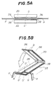
- Figs. 5A and 5B show a semiconductor device according to a second embodiment of the present invention.
- parts that are similar to parts shown in the previous described figures are given the same reference numbers as previously.
- the main surfaces of the chips 20 and 22 are located so that they are opposite to each other.
- the second embodiment of the present invention differs from the first embodiment thereof.
- the pins P extend in a straight manner inside a gap between the chips 20 and 22. In other words, the pins P are interposed between the chips 20 and 22.
- the pins P are connected to the bumps D and D', which project above the surface levels of the insulating films 26 and 28 formed on the chips 20 and 22, respectively.
- the assembly shown in Figs. 5A and 5B are sealed in the same manner as shown in Fig. 2E. Hence, the spacings and gaps are filled with resin.
- Fig. 6 shows a variation of the second embodiment of the present invention.
- parts that are similar to parts shown in the previously described figures are given the same reference numbers as previously.
- the main surfaces of the chips 20 and 22 are opposite to each other.
- the variation shown in Fig. 6 includes TAB leads R and R', which have first ends connected to the pins P and second ends connected to the bumps D and D'.
- the TAB leads R connected to the bumps D of the chip 20 are spaced apart from the TAB leads R' connected to the bumps D' of the chip 22. Further, the TAB leads R connected to the bumps D of the chip 20 are spaced apart from the insulating film 26 formed on the main surface of the chip 20.
- the TAB leads R' connected to the bumps D' of the chip 22 are spaced apart from the insulating film 28 formed on the main surface of the chip 22.
- the TAB leads R and R' may be in contact with the insulating films 26 and 28.
- the assembly shown in Fig. 6 is them sealed in mold resin so that only the pins (outer leads) P project from the package. Hence, the spacings and gaps are filled with resin.
- the semiconductor device comprises chips 20A and 22A, which have identical circuit arrangements.
- a plurality of bumps or pads D formed on the chip 20A are arranged in a line in the direction perpendicular to the longitudinal direction of the chip 20A.
- bumps D4, D3, D5, D2, D6, D1, D14, D8, D12, D9, D10, and D11 are aligned in this order from the left side of the chip 20A shown in Fig. 7A.
- Insulating films 26B made of, for example, polyimide, are formed on the main surface of the chip 20A so that the bumps D are interposed between the insulating films 26B.
- the bumps D are connected to the corresponding pins P by TAB leads R, which extend on or above the insulating films 26B.
- a plurality of bumps or pads D' formed on the chip 22A are arranged in a line in the direction perpendicular to the longitudinal direction of the chip 22A.
- bumps D4', D3', D5', D2', D6', D1', D14', D8', D12', D9', D10', and D11' are aligned in this order from the right side of the chip 22A shown in Fig. 7B. That is, the chip 22A shown in Fig. 7B corresponds to the chip 20A shown in Fig. 7A when the chip 20A is rotated by 180°.
- Insulating films 28B made of, for example, polyimide, are formed on the main surface of the chip 22A so that the bumps D' are interposed between the insulating films 28B.
- the bumps D' are connected to the corresponding pins P by TAB leads R', which extend on or above the insulating films 28B.
- the chips 20A and 22A can be connected to the pins P so that the back surfaces thereof are opposite to each other. It is also possible to position the chips 20A and 22A so that the main surfaces thereof are opposite to each other.
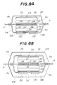
- Figs. 8A and 8B show a semiconductor device according to a fourth embodiment of the present invention.
- the semiconductor device shown in Figs. 8A and 8B is based on the structures shown in Figs. 4A and 5A. More specifically, the semiconductor device comprises four chips 20, 22, 120 and 122 having identical circuit arrangements. The back surfaces of the chips 20 and 22 are in contact with each other, and the back surfaces of the chips 120 and 122 are in contact with each other.
- TAB leads Ra have first ends connected to the pins P, and second ends connected to the bumps D formed on the main surface of the chip 20.
- the pins P extend in the gap between the chips 22 and 120, and are connected to the bumps D' formed on the main surface of the chip 22.
- the pins P are also connected to bumps Db formed on the main surface of the chip 120.
- TAB leads Rb have first ends connected to the pins P, and second ends connected to bumps Db' formed on the main surface of the chip 122.
- the bumps D, D', Db and Db' are arranged in a line on the main surfaces of the chips 20, 22, 120 and 122, as shown in Figs. 3A and 3B.
- TAB tapes 130 connected to the TAB leads Rb can be omitted.
- the chip size of the semiconductor device shown in Figs. 8A and 8B is the same as that of the semiconductor device shown in Fig. 4A. However, the storage capacity of the semiconductor device shown in Figs. 8A and 8B is twice the storage capacity of the semiconductor device shown in Fig. 4A.
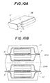
- Fig. 9 shows a semiconductor device according to a fifth embodiment of the present invention.
- TAB leads Rd have first ends connected to the pins P, and second ends connected to the bumps D' formed on the main surface of the chip 22.
- TAB leads Re have first ends connected to the pins, and second ends connected to the bumps Db formed on the main surface of the chip 120.
- the chip 20 is located above the chip 22 and is supported by TAB leads Rc, which have first ends connected to the pins P, and second ends connected to the bumps D formed on the main surface of the chip 20.
- the chip 122 is located below the chip 120 and is supported by TAB leads Rf, which have first ends connected to the pins P, and second ends connected to the bumps Db' formed on the main surface of the chip 122.
- Insulating TAB tapes 132 attached to the TAB leads Rd are opposite to the back surface of the chip 20, and insulating TAB tapes 134 attached to the TAB leads Re are opposite to the back surface of the chip 122.
- the four chips 20, 22, 120 and 122 are supported by and connected to the TAB leads.
- the two chips 22 and 120 are supported to and connected to the pins P, and the remaining two chips 20 and 122 are supported to and connected to the TAB leads Ra and Rb. It is possible to provide insulating films on the main surfaces of the chips 20, 22, 120 and 122.
- the assembly shown in Fig. 9 is sealed as in the case of the semiconductor device shown in Fig. 8B. The gaps and spaces in the assembly are filled with resin.
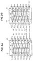
- Figs. 10A and 10B illustrate a semiconductor device according to a sixth embodiment of the present invention.
- the semiconductor device according to the sixth embodiment comprises two assemblies A1 and A2, each of which has the same structure as shown in Fig. 8B.
- the assembly A1 having pins P' is sealed in a package 124A of resin formed so that it has a trapezoidal cross section.
- the assembly A2 having pins P is sealed in a package 124B of resin formed so that it has the almost the same trapezoidal cross section as the package 124A.
- the package 124A and the package 124B are fastened to each other by, for example, an adhesive.
- the assemblies A1 and A2 can be sealed at a time.
- the pins P' are curved upwards
- the pins P are curved downwards.
- the bumps D are arranged in a line l, as shown in Fig. 11A.
- the present invention can be applied to various integrated circuits.
- the most typical example is a memory device, such as a DRAM or SRAM device.
- the chip select terminals can be omitted.
- bonding wires in lieu of the TAB leads. It is also possible for the pins or leads to have curved portions, as disclosed in the aforementioned international publication.
Landscapes
- Engineering & Computer Science (AREA)
- Microelectronics & Electronic Packaging (AREA)
- Power Engineering (AREA)
- Computer Hardware Design (AREA)
- Physics & Mathematics (AREA)
- Condensed Matter Physics & Semiconductors (AREA)
- General Physics & Mathematics (AREA)
- Wire Bonding (AREA)
Abstract
A semiconductor device includes a first chip (20, 20A, 120) having a circuit arrangement, and a plurality of first terminals (D) formed on a main surface of the first chip and substantially arranged into a line. The semiconductor device also includes a second chip (22, 22A, 122) having a circuit arrangement identical to that of the first chip, and a plurality of second terminals (D') formed on a main surface of the second chip and substantially arranged into a line. The first and second chips are arranged in a predetermined direction perpendicular to the main surfaces of the first and second chips. The semiconductor device also includes a plurality of connecting members (R, R', P) connected to the first terminals and the second terminals and provided for external connections.
Description
- The present invention generally relates to semiconductor devices, and more particularly to a semiconductor device having a plurality of chips sealed in a package.
- The storage capacity of semiconductor storage devices increases by a factor of four times every three years. The storage capacity obtainable in a generation depends on the level of the lithographic technology achieved in the generation. Recently, it has been required to provide compact, less-expensive, advanced information processing devices. These devices need an increased storage capacity.
- In order to increase the storage capacity of the above devices , a semiconductor device has been proposed in which a plurality of chips are sealed in a package (see WO 91/14282). Conventionally, chips of two different types having a mirror symmetry relationship must be provided. Hence, it is not easy to efficiently produce the semiconductor devices having the packaged chips.
- Figs. 1A, 1B and 1C show a conventional semiconductor device having a plurality of chips. The semiconductor device shown in Figs. 1A, 1B and 1C includes two
chips chip 10 has a main surface 10a on which circuit elements are arranged, and a back surface 10b. Similarly, thechip 12 has amain surface 12a on which circuit elements are arranged, and a back surface 12b. Thechips single package 14. Thechips mark 16 indicates one of two types of circuit arrangements, and amark 18 indicates the other circuit arrangement type. - Bumps or pads D1 - D6 and D8 - D12 are provided on the
chip 10, and are connected to pins P1 - P6 and P8 - P12 by leads (bonding, for example) R1 - R6 and R8 - R12, respectively. Bumps or pads D1' - D6' and D8' - D12' are provided on thechip 12, and are connected to pins P1' - P6' and P8' - P12' by leads (bonding, for example) R1' - R6' and R8' - R12', respectively. Pin P7 are non-connecting pins which are not connected to thechips chip 10 and a bump D14' of thechip 12 by leads R13 and R14', respectively. - The pins P1 - P6 and P8 - P12 other than the pins P13 and P14 are respectively connected to the bumps D1 - D6 and D8 - D12 formed on the
chip 10 and are further connected to the bumps D1' - D6' and D8' - D12', respectively. The semiconductor device shown in Figs. 1A - 1C has a storage capacity approximately equal to twice the storage capacity of the conventional semiconductor device having a package size equal to that of the conventional semiconductor device. - The semiconductor device shown in Figs. 1A - 1C uses the two different types of chips. That is, the two different circuit arrangements having the mirror symmetry relationship are used. Hence, two different mask patterns must be prepared though the sequences of the production steps for the
chips - It is a general object of the present invention to provide a semiconductor device having a plurality of chips in which the above disadvantages are eliminated.
- A more specific object of the present invention is to provide a semiconductor device having a plurality of chips which have identical circuit arrangements and which are sealed in a package.
- The above objects of the present invention are achieved by a semiconductor device comprising: a first chip having a circuit arrangement, and a plurality of first terminals formed on a main surface of the first chip and substantially arranged into a line; a second chip having a circuit arrangement identical to that of the first chip, and a plurality of second terminals formed on a main surface of the second chip and substantially arranged into a line, the first and second chips being arranged in a predetermined direction perpendicular to the respective main surfaces of the first and second chips; and a plurality of connecting members connected to the first terminals and the second terminals and provided for external connections.
- The above objects of the present invention are also achieved by a semiconductor device comprising: a plurality of chips respectively having main surfaces and an identical circuit arrangement, the chips being arranged in a predetermined direction perpendicular to the main surfaces of the chips, each of the chips having a plurality of terminals formed on the main surface and substantially arranged in a line; and a plurality of connecting members connected to the terminals of the chips and provided for external connections, a first one of the chips having a back surface opposite to the main surface thereof, a second one of the chips having a back surface opposite to the main surface thereof, and the back surface of the first one of the chips being in contact with the back surface of the second one of the chips.
- The above objects of the present invention are also achieved by a semiconductor device comprising: a plurality of chips respectively having main surfaces and an identical circuit arrangement, the chips being arranged in a predetermined direction perpendicular to the main surfaces of the chips, each of the chips having a plurality of terminals formed on the main surface and substantially arranged in a line; and a plurality of connecting members connected to the terminals of the chips to an external device, the chips being grouped into a plurality of groups; each of the groups comprising a first one of the chips having a back surface opposite to the main surface thereof, and a second one of the chips having a back surface opposite to the main surface thereof, and the back surface of the first one of the chips being in contact with the back surface of the second one of the chips.
- Other objects, features and advantages of the present invention will become more apparent from the following detailed description when read in conjunction with the accompanying drawings, in which:
- Fig. 1A is a plan view of a type of a chip used in a conventional semiconductor device having a plurality of chips;
- Fig. 1B is a plan view of a chip of a type different from that of the chip shown in Fig. 1B and used in the conventional semiconductor device;
- Fig. 1C is a cross-sectional view of the conventional semiconductor device having the chips shown in Figs. 1A and 1B;
- Fig. 2A is a plan view of a first chip used in a semiconductor device according to a first embodiment of the present invention;
- Fig. 2B is a plan view of a second chip used in the first embodiment of the present invention;
- Fig. 2C is a cross-sectional view of the semiconductor device according to the first embodiment of the present invention;
- Fig. 2D is a perspective view of the semiconductor device according to the first embodiment of the present invention;
- Fig. 2E is a cross sectional view of the semiconductor device in which the chips are sealed in a package of resin;
- Fig. 3A is a plan view of the first chip used in the first embodiment of the present invention;
- Fig. 3B is a plan view of the second chip used in the first embodiment of the present invention;
- Fig. 4A is a cross-sectional view of a first variation of the first embodiment of the present invention;
- Fig. 4B is a cross-sectional view of a second variation of the first embodiment of the present invention;
- Fig. 5A is a cross-sectional view of a semiconductor device according to a second embodiment of the present invention;
- Fig. 5B is a perspective view of the semiconductor device according to the second embodiment of the present invention;
- Fig. 6 is a cross-sectional view of a variation of the second embodiment of the present invention;
- Fig. 7A is a plan view of a first chip used in a semiconductor device according to a third embodiment of the present invention;
- Fig. 7B is a plan view of a second chip used in the semiconductor device according to the third embodiment of the present invention;
- Fig. 8A is a cross-sectional view of a semiconductor device according to a fourth embodiment of the present invention;
- Fig. 8B is a cross-sectional view of the semiconductor device of the fourth embodiment having a molded package;
- Fig. 9 is a cross-sectional view of a semiconductor device according to a fifth embodiment of the present invention;
- Fig. 10A is a perspective view of a semiconductor device according to a sixth embodiment of the present invention;
- Fig. 10B is a cross-sectional view of the semiconductor device according to the sixth embodiment of the present invention;
- Fig. 11A is a diagram showing an arrangement of bumps used in the embodiments of the present invention; and
- Fig. 11B is a diagram showing an alternative arrangement of bumps used in the embodiments of the present invention.
- Figs. 2A, 2B, 2C and 2D are diagrams showing a semiconductor device according to a first embodiment of the present invention. The semiconductor device shown in Figs. 2A - 2D comprises two
chips chip 20 has a main surface 20a on which circuit elements are arranged, and a back surface 20b. Thechip 22 has amain surface 22a on which circuit elements are arranged, and a back surface 22b. As shown in Fig. 2C, the back surfaces 20b and 22b of thechips chip 20 is the same as that of thechip 22. In other words, the circuit arrangements of thechips - As shown in Fig. 2A, insulating
films 26 are formed on the main surface 20a of thechip 20 so that a gap defined by the insulatingfilms 26 extends in the longitudinal direction of thechip 20. Similarly, insulatingfilms 28 are formed on themain surface 22a of thechip 22 so that a gap defined by the insulatingfilms 26 extends in the longitudinal direction of thechip 22. As shown in Fig. 2C, the insulatingfilms 26 are in contact with the main surface 20a of thechip 20, and the insulatingfilms 28 are in contact with themain surface 22a of thechip 22. - As shown in Fig. 3A, the plurality of bumps or pads D1, D8, D2, D9, D3, D10, D4, D11, D5, D12, D6 and D13 are aligned on the
chip 20 and located at the center portion of thechip 20 between the insulatingfilms 26. As shown in Fig. 3B, the plurality of bumps or pads D1', D8', D2', D9', D3', D10', D4', D11', D5', D12', D6' and D14' are aligned on thechip 22 and located at the center portion of thechip 22 between the insulatingfilms 28. - The bumps D1 - D6 and D8 - D13 are connected to the pins P1 - P6 and P8 - P13 by the leads R1 - R6 and R8 - R13, respectively. These leads are, for example, TAB (Tape Automated Bonding) leads. The bumps D1' - D6', D8' - D12' and D14' are connected to pins the P1 - P6, P8 - P12 and P14 by the leads R1' - R6', R8' - R12' and R14', respectively. These leads are, for example, TAB leads. In Fig. 2C, four TAB leads are indicated by R and R', and two bumps are indicated by D and D'. The TAB leads R and R' extend on the insulating
films films chips films chips films - Pins P7 shown in Figs. 2A and 2B are non-connecting pins which are not connected to circuits of the
chips chips chip 20 is connected to the bump D13, while the chip select pin P14 thereof is not connected to any bump. The chip select pin P14 of thechip 22 is connected to the bump D14', and the chip select pin P13 thereof is not connected to any bump. When a chip select signal is externally applied to the pins P13 of thechips chip 20 is selected. When a chip select signal is externally applied to the pins P14 of thechips chip 22 is selected. - The semiconductor device according to the first embodiment of the present invention can be produced by the following process. First ends of the TAB leads R and R' are connected to the bumps D and D' formed on the
chips chip 20 are connected to a lead frame having lead projections by using a bonding tool. In practice, a plurality ofchips 20 are fastened to the lead frame at a time. Thereafter, the second ends of the TAB leads R' of thechip 22 are connected to the lead frame so that the back surfaces of thechips chips chips 22 are fastened to the lead frame at a time. Then, the assembly is sealed in apackage 24 of a molded resin, as shown in Fig. 2E. - Fig. 4A is a cross-sectional view of a first variation of the first embodiment of the present invention. The insulating
films 26 made of, for example, polyimide, are spaced apart from the TAB leads R, and the insulatingfilms 28 are spaced apart from the TAB leads R'. The bumps D and D' project above the surface levels of the insulatingfilms TAB tapes 30 are attached to the TAB leads R'. It is possible to omit the insulatingTAB tapes 30. - Fig. 4B is a cross-sectional view of a second variation of the first embodiment of the present invention. The second variation shown in Fig. 4B employs a multi-layer tape consisting of a TAB lead and an insulating TAB tape. As shown in Fig. 4B, insulating
TAB tapes 26A, which are patterned, are connected to the TAB leads R related to thechip 20, and are spaced apart from thechip 20. Alternatively, the insulatingTAB tapes 26A may be in contact with the main surface of thechip 20. Similarly, insulatingTAB tapes 28A, which are patterned, are connected to the TAB leads R' related to thechip 22, and are spaced apart from thechip 22. Alternatively, the insulatingTAB tapes 28A may be in contact with the main surface of thechip 22. A character G indicates a gap between each of thechips TAB tapes - Figs. 5A and 5B show a semiconductor device according to a second embodiment of the present invention. In Figs. 5A and 5B, parts that are similar to parts shown in the previous described figures are given the same reference numbers as previously. The main surfaces of the
chips chips chips films chips - Fig. 6 shows a variation of the second embodiment of the present invention. In Fig. 6, parts that are similar to parts shown in the previously described figures are given the same reference numbers as previously. The main surfaces of the
chips chip 20 are spaced apart from the TAB leads R' connected to the bumps D' of thechip 22. Further, the TAB leads R connected to the bumps D of thechip 20 are spaced apart from the insulatingfilm 26 formed on the main surface of thechip 20. Similarly, the TAB leads R' connected to the bumps D' of thechip 22 are spaced apart from the insulatingfilm 28 formed on the main surface of thechip 22. The TAB leads R and R' may be in contact with the insulatingfilms - A description will now be given of a semiconductor device according to a third embodiment of the present invention with reference to Figs. 7A and 7B, in which parts that are similar to parts shown in the previously described figures are given the same reference numbers.
- The semiconductor device according to the third embodiment of the present invention comprises
chips chip 20A are arranged in a line in the direction perpendicular to the longitudinal direction of thechip 20A. In Fig. 7A, bumps D4, D3, D5, D2, D6, D1, D14, D8, D12, D9, D10, and D11 are aligned in this order from the left side of thechip 20A shown in Fig. 7A. Insulatingfilms 26B made of, for example, polyimide, are formed on the main surface of thechip 20A so that the bumps D are interposed between the insulatingfilms 26B. The bumps D are connected to the corresponding pins P by TAB leads R, which extend on or above the insulatingfilms 26B. - A plurality of bumps or pads D' formed on the
chip 22A are arranged in a line in the direction perpendicular to the longitudinal direction of thechip 22A. In Fig. 7B, bumps D4', D3', D5', D2', D6', D1', D14', D8', D12', D9', D10', and D11' are aligned in this order from the right side of thechip 22A shown in Fig. 7B. That is, thechip 22A shown in Fig. 7B corresponds to thechip 20A shown in Fig. 7A when thechip 20A is rotated by 180°. Insulatingfilms 28B made of, for example, polyimide, are formed on the main surface of thechip 22A so that the bumps D' are interposed between the insulatingfilms 28B. The bumps D' are connected to the corresponding pins P by TAB leads R', which extend on or above the insulatingfilms 28B. - The
chips chips - It will be noted that various variations and modification can be made on the basis of the above-described semiconductor devices, each having two chips.
- Figs. 8A and 8B show a semiconductor device according to a fourth embodiment of the present invention. In Figs. 8A and 8B, parts that are the same as parts shown in the previously described figures are given the same reference numbers. The semiconductor device shown in Figs. 8A and 8B is based on the structures shown in Figs. 4A and 5A. More specifically, the semiconductor device comprises four
chips chips chips chip 20. The pins P extend in the gap between thechips chip 22. The pins P are also connected to bumps Db formed on the main surface of thechip 120. TAB leads Rb have first ends connected to the pins P, and second ends connected to bumps Db' formed on the main surface of thechip 122. The bumps D, D', Db and Db' are arranged in a line on the main surfaces of thechips TAB tapes 130 connected to the TAB leads Rb can be omitted. The chip size of the semiconductor device shown in Figs. 8A and 8B is the same as that of the semiconductor device shown in Fig. 4A. However, the storage capacity of the semiconductor device shown in Figs. 8A and 8B is twice the storage capacity of the semiconductor device shown in Fig. 4A. - Fig. 9 shows a semiconductor device according to a fifth embodiment of the present invention. In Fig. 9, parts that are the same as parts shown in the previously described figures are given the same reference numbers. The back surfaces of the
chips chip 22. TAB leads Re have first ends connected to the pins, and second ends connected to the bumps Db formed on the main surface of thechip 120. - The
chip 20 is located above thechip 22 and is supported by TAB leads Rc, which have first ends connected to the pins P, and second ends connected to the bumps D formed on the main surface of thechip 20. Thechip 122 is located below thechip 120 and is supported by TAB leads Rf, which have first ends connected to the pins P, and second ends connected to the bumps Db' formed on the main surface of thechip 122. InsulatingTAB tapes 132 attached to the TAB leads Rd are opposite to the back surface of thechip 20, and insulatingTAB tapes 134 attached to the TAB leads Re are opposite to the back surface of thechip 122. - According to the fifth embodiment of the present invention, the four
chips chips chips chips - Figs. 10A and 10B illustrate a semiconductor device according to a sixth embodiment of the present invention. As shown in Fig. 10B, the semiconductor device according to the sixth embodiment comprises two assemblies A1 and A2, each of which has the same structure as shown in Fig. 8B. The assembly A1 having pins P' is sealed in a package 124A of resin formed so that it has a trapezoidal cross section. Similarly, the assembly A2 having pins P is sealed in a package 124B of resin formed so that it has the almost the same trapezoidal cross section as the package 124A. The package 124A and the package 124B are fastened to each other by, for example, an adhesive. Alternatively, the assemblies A1 and A2 can be sealed at a time. As shown in Fig. 10A, the pins P' are curved upwards, and the pins P are curved downwards.
- It can be seen from the above that a large number of combinations of the embodiments can be made.
- In the above description, the bumps D are arranged in a line l, as shown in Fig. 11A. However, it is possible to arrange the bumps D so that the bumps D slightly deviate from the line l, as shown in Fig. 11B. If the bumps D greatly deviate from the line l, the condition of the connections between the bumps and the pins of one chip will be greatly different from that of the connections between the bumps and the pins of an other chip. In this case, the resistances, inductances or capacitances of the TAB leads of two or more chips will be different from each other.
- The present invention can be applied to various integrated circuits. The most typical example is a memory device, such as a DRAM or SRAM device. In some applications, the chip select terminals can be omitted.
- It is possible to use bonding wires in lieu of the TAB leads. It is also possible for the pins or leads to have curved portions, as disclosed in the aforementioned international publication.
- The present invention is not limited to the specifically disclosed embodiments, and variations and modifications may be made without departing from the scope of the present invention.
Claims (32)
- A semiconductor device comprising:
a first chip (20, 20a, 120) having a circuit arrangement, and a plurality of first terminals (D) formed on a main surface of the first chip and substantially arranged into a line;
a second chip (22, 22A, 122) having a circuit arrangement identical to that of the first chip, and a plurality of second terminals (D') formed on a main surface of the second chip and substantially arranged into a line, the first and second chips being arranged in a predetermined direction perpendicular to the main surfaces of the first and second chips; and
a plurality of connecting members (R, R', P) connected to the first terminals and the second terminals and provided for external connections. - The semiconductor device as claimed in claim 1, characterized in that:
each of the first and second chips has a rectangular shape;
the first terminals are arranged in a line in a longitudinal direction of the first chip; and
the second terminals are arranged in a line in a longitudinal direction of the second chip. - The semiconductor device as claimed in claim 1, characterized in that:
each of the first and second chips has a rectangular shape;
the first terminals are arranged in a line in a direction perpendicular to a longitudinal direction of the first chip; and
the second terminals are arranged in a line in a direction perpendicular to a longitudinal direction of the second chip. - The semiconductor device as claimed in claim 1, characterized in that:
the first chip has a back surface opposite to the main surface thereof;
the second chip has a back surface opposite to the main surface thereof; and
the back surface of the first chip is in contact with the back surface of the second chip. - The semiconductor device as claimed in claim 1, characterized in that the first chip and second chip are arranged in the predetermined direction so that the main surface of the first chip is opposite to the main surface of the second chip.
- The semiconductor device as claimed in claim 1, characterized in that said connecting members comprise:
a plurality of lead members for external connections; and
tape-automated bonding leads connecting the first and second terminals to the lead members. - The semiconductor device as claimed in claim 1, characterized by further comprising:
a first insulating member provided between the main surface of the first chip and the connecting members connected to the first terminals formed on the main surface of the first chip; and
a second insulating member provided between the main surface of the second chip and the connecting members connected to the second terminals formed on the main surface of the second chip. - The semiconductor device as claimed in claim 7, characterized in that:
the first insulating member is in contact with the main surface of the first chip; and
the second insulating member is in contact with the main surface of the second chip. - The semiconductor device as claimed in claim 7, characterized in that:
the first insulating member is in contact with the connecting members connected to the first terminals formed on the main surface of the first chip; and
the second insulating member is in contact with the connecting members connected to the second terminals formed on the main surface of the second chip. - The semiconductor device as claimed in claim 7, characterized in that:
the first insulating member is in contact with both the main surface of the first chip and the connecting members connected to the first terminals formed on the main surface of the first chip; and
the second insulating member is in contact with both the main surface of the second chip and the connecting members connected to the second terminals formed on the main surface of the second chip. - The semiconductor device as claimed in claim 5, characterized in that the first chip and the second chip are spaced apart from each other in the predetermined direction.
- The semiconductor device as claimed in claim 1, characterized in that:
said connecting members comprise a plurality of lead members for external connections; and
the lead members are directly connected to the first and second terminals. - The semiconductor device as claimed in claim 12, characterized in that:
the first chip and second chip are arranged in the predetermined direction so that the main surface of the first chip is opposite to the main surface of the second chip; and
the lead members extend in a straight manner between the first and second chips and in parallel with the main surfaces of the first and second chips. - The semiconductor device as claimed in claim 1, characterized in that the connecting members comprise:
a plurality of lead members for external connections; and
tape-automated bonding leads connecting the first and second terminals to the lead members, and characterized in that;
the first chip has a back surface opposite to the main surface thereof;
the second chip has a back surface opposite to the main surface thereof; and
the back surface of the first chip is in contact with the back surface of the second chip. - The semiconductor device as claimed in claim 14, characterized in that the tape-automated bonding leads comprise curved portions.
- The semiconductor device as claimed in claim 14, characterized by further comprising:
a first insulating film provided between the main surface of the first chip and the tape-automated bonding leads connected to the first terminals formed on the main surface of the first chip; and
a second insulating film provided between the main surface of the second chip and the tape-automated bonding leads connected to the second terminals formed on the main surface of the second chip. - The semiconductor device as claimed in claim 1, characterized in that the connecting members comprise:
a plurality of lead members for external connections; and
tape-automated bonding leads connecting the first and second terminals to the lead members, and characterized in that;
the first chip and second chip are arranged in the predetermined direction so that the main surface of the first chip is opposite to the main surface of the second chip. - The semiconductor device as claimed in claim 17, characterized in that the tape-automated bonding leads extend in a straight manner and in parallel with the main surfaces of the first and second chips.
- The semiconductor device as claimed in claim 17, characterized in that the tape-automated bonding leads are spaced apart from each other.
- The semiconductor device as claimed in claim 1, characterized in that the first chip and the second chip are vertically stacked so that the first chip and the second chip are spaced apart from each other in the predetermined direction.
- The semiconductor device as claimed in claim 2, characterized in that:
the first terminals are located at a center portion on the main surface of the first chip extending in the longitudinal direction of the first chip; and
the second terminals are located at a center portion on the main surface of the second chip extending in the longitudinal direction of the second chip. - The semiconductor device as claimed in claim 3, characterized in that:
the first terminals are located at a center portion on the main surface of the first chip extending in the direction perpendicular to the longitudinal direction of the first chip; and
the second terminals are located at a center portion on the main surface of the second chip extending in the direction perpendicular to the longitudinal direction of the second chip. - The semiconductor device as claimed in claim 1, characterized by further comprising a package in which the first and second chips are sealed.
- A semiconductor device comprising:
a plurality of chips (20, 22, 120, 122) respectively having main surfaces and identical circuit arrangements, the chips being arranged in a predetermined direction perpendicular to the main surfaces of the chips, each of the chips having a plurality of terminals (D, D') formed on the main surface and substantially arranged in a line; and
a plurality of connecting members (R, R' P) connected to the terminals of the chips and provided for external connections,
a first one of the chips having a back surface opposite to the main surface thereof,
a second one of the chips having a back surface opposite to the main surface thereof, and
the back surface of said first one of the chips being in contact with the back surface of said second one of the chips. - The semiconductor device as claimed in claim 24, characterized in that:
a third one of the chips has a back surface opposite to the main surface thereof;
a fourth one of the chips has a back surface to the main surface thereof;
the back surface of said third one of the chips is in contact with the back surface of said fourth one of the chips;
the first, second, third and fourth ones of the chips are arranged in this order in the predetermined direction; and
the main surface of the second one of the chips is opposite to the main surface of the third one of the chips. - The semiconductor device as claimed in claim 24, characterized in that:
the connecting members comprise lead members for external connections, and tape-automated bonding leads provided for the first and fourth ones of the chips;
the lead members have ends connected to the terminals formed on the main surfaces of the second and third ones of the chips; and
tape-automated bonding leads have first ends connected to the terminals formed on the main surfaces of the first and fourth ones of the chips, and second ends connected to the lead members. - The semiconductor device as claimed in claim 26, characterized by further comprising:
a first insulating film provided between the main surface of said first one of the chips and the tape-automated bonding leads connected to the terminals formed on the main surface of said first one of the chips;
a second insulating film provided between the main surface of said second one of the chips and the lead members connected to the terminals formed on the main surface of said second one of the chips;
a third insulating film provided between the main surface of said third one of the chips and the lead members connected to the terminals formed on the main surface of said third one of the chips; and
a fourth insulating film provided between the main surface of said fourth tone of the chips and the tape-automated bonding leads connected to the terminals formed on the main surface of said fourth one of the chips. - The semiconductor device as claimed in claim 27, characterized in that:
the first insulating film is in contact with the main surface of said first one of the chips;
the second insulating film is in contact with the main surface of said second one of the chips;
the third insulating film is in contact with the main surface of said third one of the chips; and
the fourth insulating film is in contact with the main surface of said fourth one of the chips. - The semiconductor device as claimed in claim 24, characterized in that:
a third one of the chips has a back surface opposite to the main surface thereof;
a fourth one of the chips has a back surface to the main surface thereof;
the first, second, third and fourth ones of the chips are arranged in this order in the predetermined direction;
the main surface of the second one of the chips is opposite to the main surface of the third one of the chips;
the back surface of said first one of the chips is opposite to the main surface of said second one of the chips; and
the back surface of said fourth one of the chips is opposite to the main surface of said third one of the chips. - The semiconductor device as claimed in claim 29, characterized in that:
the connecting members comprise first, second, third and fourth tape-automated bonding leads, and lead members;
the first tape-automated bonding leads connect the lead frames to the terminals formed on the main surface of said first one of the chips;
the second tape-automated bonding leads connect the lead frames to the terminals formed on the main surface of said second one of the chips;
the third tape-automated bonding leads connect the lead frames to the terminals formed on the main surface of said third one of the chips; and
the fourth tape-automated bonding leads connect the lead frames to the terminals formed on the main surface of said fourth one of the chips. - The semiconductor device as claimed in claim 24, characterized by further comprising a package in which the chips are sealed.
- A semiconductor device comprising:
a plurality of chips respectively having main surfaces and identical circuit arrangements, the chips being arranged in a predetermined direction perpendicular to the main surfaces of the chips, each of the chips having a plurality of terminals formed on the main surface and substantially arranged in a line; and
a plurality of connecting members connected to the terminals of the chips and provided for external connections,
the chips being grouped into a plurality of groups;
each of the groups comprising a first one of the chips having a back surface opposite to the main surface thereof, and a second one of the chips having a back surface opposite to the main surface thereof, and
the back surface of said first one of the chips being in contact with the back surface of said second one of the chips.
Priority Applications (2)
| Application Number | Priority Date | Filing Date | Title |
|---|---|---|---|
| EP92121643A EP0608440A1 (en) | 1992-12-18 | 1992-12-18 | Semiconductor device having a plurality of chips having identical circuit arrangements sealed in package |
| US08/355,985 US5508565A (en) | 1992-12-18 | 1994-12-14 | Semiconductor device having a plurality of chips having identical circuit arrangement sealed in package |
Applications Claiming Priority (2)
| Application Number | Priority Date | Filing Date | Title |
|---|---|---|---|
| EP92121643A EP0608440A1 (en) | 1992-12-18 | 1992-12-18 | Semiconductor device having a plurality of chips having identical circuit arrangements sealed in package |
| US08/355,985 US5508565A (en) | 1992-12-18 | 1994-12-14 | Semiconductor device having a plurality of chips having identical circuit arrangement sealed in package |
Publications (1)
| Publication Number | Publication Date |
|---|---|
| EP0608440A1 true EP0608440A1 (en) | 1994-08-03 |
Family
ID=26131219
Family Applications (1)
| Application Number | Title | Priority Date | Filing Date |
|---|---|---|---|
| EP92121643A Ceased EP0608440A1 (en) | 1992-12-18 | 1992-12-18 | Semiconductor device having a plurality of chips having identical circuit arrangements sealed in package |
Country Status (2)
| Country | Link |
|---|---|
| US (1) | US5508565A (en) |
| EP (1) | EP0608440A1 (en) |
Cited By (1)
| Publication number | Priority date | Publication date | Assignee | Title |
|---|---|---|---|---|
| WO2006010903A2 (en) * | 2004-07-30 | 2006-02-02 | University Of Kent | Multiple chip semiconductor device |
Families Citing this family (57)
| Publication number | Priority date | Publication date | Assignee | Title |
|---|---|---|---|---|
| JP2634516B2 (en) * | 1991-10-15 | 1997-07-30 | 三菱電機株式会社 | Manufacturing method of inverted IC, inverted IC, IC module |
| JP3299342B2 (en) * | 1993-06-11 | 2002-07-08 | 株式会社日立製作所 | Semiconductor memory module |
| US6191368B1 (en) | 1995-09-12 | 2001-02-20 | Tessera, Inc. | Flexible, releasable strip leads |
| TW520816U (en) * | 1995-04-24 | 2003-02-11 | Matsushita Electric Ind Co Ltd | Semiconductor device |
| US5677567A (en) * | 1996-06-17 | 1997-10-14 | Micron Technology, Inc. | Leads between chips assembly |
| US5994166A (en) * | 1997-03-10 | 1999-11-30 | Micron Technology, Inc. | Method of constructing stacked packages |
| US6271582B1 (en) | 1997-04-07 | 2001-08-07 | Micron Technology, Inc. | Interdigitated leads-over-chip lead frame, device, and method for supporting an integrated circuit die |
| US6008996A (en) | 1997-04-07 | 1999-12-28 | Micron Technology, Inc. | Interdigitated leads-over-chip lead frame, device, and method for supporting an integrated circuit die |
| US6028352A (en) * | 1997-06-13 | 2000-02-22 | Irvine Sensors Corporation | IC stack utilizing secondary leadframes |
| US5986209A (en) | 1997-07-09 | 1999-11-16 | Micron Technology, Inc. | Package stack via bottom leaded plastic (BLP) packaging |
| US5923959A (en) * | 1997-07-23 | 1999-07-13 | Micron Technology, Inc. | Ball grid array (BGA) encapsulation mold |
| US6472252B2 (en) * | 1997-07-23 | 2002-10-29 | Micron Technology, Inc. | Methods for ball grid array (BGA) encapsulation mold |
| US6096576A (en) | 1997-09-02 | 2000-08-01 | Silicon Light Machines | Method of producing an electrical interface to an integrated circuit device having high density I/O count |
| JP3937265B2 (en) | 1997-09-29 | 2007-06-27 | エルピーダメモリ株式会社 | Semiconductor device |
| US6144089A (en) | 1997-11-26 | 2000-11-07 | Micron Technology, Inc. | Inner-digitized bond fingers on bus bars of semiconductor device package |
| US6509632B1 (en) | 1998-01-30 | 2003-01-21 | Micron Technology, Inc. | Method of fabricating a redundant pinout configuration for signal enhancement in an IC package |
| US6114756A (en) | 1998-04-01 | 2000-09-05 | Micron Technology, Inc. | Interdigitated capacitor design for integrated circuit leadframes |
| JPH11307719A (en) * | 1998-04-20 | 1999-11-05 | Mitsubishi Electric Corp | Semiconductor device |
| SG75958A1 (en) | 1998-06-01 | 2000-10-24 | Hitachi Ulsi Sys Co Ltd | Semiconductor device and a method of producing semiconductor device |
| US6303986B1 (en) | 1998-07-29 | 2001-10-16 | Silicon Light Machines | Method of and apparatus for sealing an hermetic lid to a semiconductor die |
| JP2000183701A (en) | 1998-12-18 | 2000-06-30 | Nec Ic Microcomput Syst Ltd | Semiconductor integrated circuit and method for preventing deterioration of duty |
| US6265771B1 (en) * | 1999-01-27 | 2001-07-24 | International Business Machines Corporation | Dual chip with heat sink |
| US6476499B1 (en) | 1999-02-08 | 2002-11-05 | Rohm Co., | Semiconductor chip, chip-on-chip structure device and assembling method thereof |
| KR100333388B1 (en) * | 1999-06-29 | 2002-04-18 | 박종섭 | chip size stack package and method of fabricating the same |
| JP2001053243A (en) * | 1999-08-06 | 2001-02-23 | Hitachi Ltd | Semiconductor memory device and memory module |
| WO2001015228A1 (en) * | 1999-08-19 | 2001-03-01 | Seiko Epson Corporation | Wiring board, method of manufacturing wiring board, electronic device, method of manufacturing electronic device, circuit board and electronic apparatus |
| US6281043B1 (en) | 1999-08-24 | 2001-08-28 | General Semiconductor, Inc. | Fabrication of hybrid semiconductor devices |
| DE10006445C2 (en) * | 2000-02-14 | 2002-03-28 | Infineon Technologies Ag | Intermediate frame for a housing frame of semiconductor chips |
| KR100335717B1 (en) * | 2000-02-18 | 2002-05-08 | 윤종용 | High Density Memory Card |
| US6586836B1 (en) * | 2000-03-01 | 2003-07-01 | Intel Corporation | Process for forming microelectronic packages and intermediate structures formed therewith |
| DE10023823A1 (en) * | 2000-05-15 | 2001-12-06 | Infineon Technologies Ag | Multi-chip housing device has carrier supporting stacked chip components with lowermost chip component having contact coupled to terminal surface of carrier |
| US6597593B1 (en) * | 2000-07-12 | 2003-07-22 | Sun Microsystems, Inc. | Powering IC chips using AC signals |
| SG102591A1 (en) | 2000-09-01 | 2004-03-26 | Micron Technology Inc | Dual loc semiconductor assembly employing floating lead finger structure |
| US6707591B2 (en) | 2001-04-10 | 2004-03-16 | Silicon Light Machines | Angled illumination for a single order light modulator based projection system |
| US6664618B2 (en) * | 2001-05-16 | 2003-12-16 | Oki Electric Industry Co., Ltd. | Tape carrier package having stacked semiconductor elements, and short and long leads |
| US6782205B2 (en) | 2001-06-25 | 2004-08-24 | Silicon Light Machines | Method and apparatus for dynamic equalization in wavelength division multiplexing |
| US6747781B2 (en) | 2001-06-25 | 2004-06-08 | Silicon Light Machines, Inc. | Method, apparatus, and diffuser for reducing laser speckle |
| KR100415279B1 (en) * | 2001-06-26 | 2004-01-16 | 삼성전자주식회사 | Chip stack package and manufacturing method thereof |
| US6829092B2 (en) | 2001-08-15 | 2004-12-07 | Silicon Light Machines, Inc. | Blazed grating light valve |
| US20030048624A1 (en) * | 2001-08-22 | 2003-03-13 | Tessera, Inc. | Low-height multi-component assemblies |
| US6800238B1 (en) | 2002-01-15 | 2004-10-05 | Silicon Light Machines, Inc. | Method for domain patterning in low coercive field ferroelectrics |
| US6767751B2 (en) | 2002-05-28 | 2004-07-27 | Silicon Light Machines, Inc. | Integrated driver process flow |
| US6728023B1 (en) | 2002-05-28 | 2004-04-27 | Silicon Light Machines | Optical device arrays with optimized image resolution |
| US6822797B1 (en) | 2002-05-31 | 2004-11-23 | Silicon Light Machines, Inc. | Light modulator structure for producing high-contrast operation using zero-order light |
| US6829258B1 (en) | 2002-06-26 | 2004-12-07 | Silicon Light Machines, Inc. | Rapidly tunable external cavity laser |
| US6813059B2 (en) | 2002-06-28 | 2004-11-02 | Silicon Light Machines, Inc. | Reduced formation of asperities in contact micro-structures |
| US6714337B1 (en) | 2002-06-28 | 2004-03-30 | Silicon Light Machines | Method and device for modulating a light beam and having an improved gamma response |
| JP2004055080A (en) * | 2002-07-23 | 2004-02-19 | Renesas Technology Corp | Semiconductor memory module and method for manufacturing semiconductor chip to be used for the same |
| US6801354B1 (en) | 2002-08-20 | 2004-10-05 | Silicon Light Machines, Inc. | 2-D diffraction grating for substantially eliminating polarization dependent losses |
| US6712480B1 (en) | 2002-09-27 | 2004-03-30 | Silicon Light Machines | Controlled curvature of stressed micro-structures |
| US6829077B1 (en) | 2003-02-28 | 2004-12-07 | Silicon Light Machines, Inc. | Diffractive light modulator with dynamically rotatable diffraction plane |
| US6806997B1 (en) | 2003-02-28 | 2004-10-19 | Silicon Light Machines, Inc. | Patterned diffractive light modulator ribbon for PDL reduction |
| DE10352946B4 (en) * | 2003-11-11 | 2007-04-05 | Infineon Technologies Ag | Semiconductor component with semiconductor chip and rewiring layer and method for producing the same |
| SG135066A1 (en) | 2006-02-20 | 2007-09-28 | Micron Technology Inc | Semiconductor device assemblies including face-to-face semiconductor dice, systems including such assemblies, and methods for fabricating such assemblies |
| US8564141B2 (en) * | 2010-05-06 | 2013-10-22 | SK Hynix Inc. | Chip unit and stack package having the same |
| US9000576B2 (en) * | 2011-04-22 | 2015-04-07 | Cyntec Co., Ltd. | Package structure and manufacturing method thereof |
| US9029234B2 (en) | 2012-05-15 | 2015-05-12 | International Business Machines Corporation | Physical design symmetry and integrated circuits enabling three dimentional (3D) yield optimization for wafer to wafer stacking |
Citations (3)
| Publication number | Priority date | Publication date | Assignee | Title |
|---|---|---|---|---|
| EP0221496A2 (en) * | 1985-11-04 | 1987-05-13 | International Business Machines Corporation | Integrated circuit package |
| EP0474224A1 (en) * | 1990-09-06 | 1992-03-11 | Hitachi, Ltd. | Semiconductor device comprising a plurality of semiconductor chips |
| DE4214102A1 (en) * | 1991-06-01 | 1992-12-03 | Gold Star Electronics | Multi-chip semiconductor module e.g. of LOC-TSOP type - has two blank chips which are interconnected by solder, while several TAB strips have each inner and outer leads |
Family Cites Families (3)
| Publication number | Priority date | Publication date | Assignee | Title |
|---|---|---|---|---|
| KR970003915B1 (en) * | 1987-06-24 | 1997-03-22 | 미다 가쓰시게 | Semiconductor device and the use memory module |
| US4956694A (en) * | 1988-11-04 | 1990-09-11 | Dense-Pac Microsystems, Inc. | Integrated circuit chip stacking |
| US5233220A (en) * | 1989-06-30 | 1993-08-03 | Texas Instruments Incorporated | Balanced capacitance lead frame for integrated circuits and integrated circuit device with separate conductive layer |
-
1992
- 1992-12-18 EP EP92121643A patent/EP0608440A1/en not_active Ceased
-
1994
- 1994-12-14 US US08/355,985 patent/US5508565A/en not_active Expired - Lifetime
Patent Citations (3)
| Publication number | Priority date | Publication date | Assignee | Title |
|---|---|---|---|---|
| EP0221496A2 (en) * | 1985-11-04 | 1987-05-13 | International Business Machines Corporation | Integrated circuit package |
| EP0474224A1 (en) * | 1990-09-06 | 1992-03-11 | Hitachi, Ltd. | Semiconductor device comprising a plurality of semiconductor chips |
| DE4214102A1 (en) * | 1991-06-01 | 1992-12-03 | Gold Star Electronics | Multi-chip semiconductor module e.g. of LOC-TSOP type - has two blank chips which are interconnected by solder, while several TAB strips have each inner and outer leads |
Cited By (2)
| Publication number | Priority date | Publication date | Assignee | Title |
|---|---|---|---|---|
| WO2006010903A2 (en) * | 2004-07-30 | 2006-02-02 | University Of Kent | Multiple chip semiconductor device |
| WO2006010903A3 (en) * | 2004-07-30 | 2006-03-09 | Univ Kent Canterbury | Multiple chip semiconductor device |
Also Published As
| Publication number | Publication date |
|---|---|
| US5508565A (en) | 1996-04-16 |
Similar Documents
| Publication | Publication Date | Title |
|---|---|---|
| US5508565A (en) | Semiconductor device having a plurality of chips having identical circuit arrangement sealed in package | |
| US5963794A (en) | Angularly offset stacked die multichip device and method of manufacture | |
| KR0147259B1 (en) | Stack type semiconductor package and method for manufacturing the same | |
| KR100606178B1 (en) | Semiconductor device having a plurality of semiconductor elements interconnected by a redistribution layer | |
| US5886412A (en) | Angularly offset and recessed stacked die multichip device | |
| US6051886A (en) | Angularly offset stacked die multichip device and method of manufacture | |
| EP0631691A1 (en) | Ic chip package and method of making same | |
| US5227995A (en) | High density semiconductor memory module using split finger lead frame | |
| JP2953899B2 (en) | Semiconductor device | |
| US6278616B1 (en) | Modifying memory device organization in high density packages | |
| KR20030055832A (en) | Stack Semiconductor Chip Package Having Multiple I/O Pins and Lead Frame Suitable For Use in Such a Stack Semiconductor Chip Package | |
| KR100585100B1 (en) | Thin semiconductor package having stackable lead frame and manufacturing method thereofLithium-sulfur battery | |
| EP0759637A2 (en) | Semiconductor package and mounting method | |
| JP3494901B2 (en) | Semiconductor integrated circuit device | |
| JP3417095B2 (en) | Semiconductor device | |
| JP2000049279A (en) | Semiconductor device | |
| US6884657B1 (en) | Angularly offset stacked die multichip device and method of manufacture | |
| EP0398628A2 (en) | Semiconductor memory device | |
| KR100520409B1 (en) | Ball grid array type multi-chip package | |
| JP2568771B2 (en) | Semiconductor device | |
| JPH09252083A (en) | Electronic device and manufacture thereof | |
| JPH02229461A (en) | Semiconductor device | |
| JP2001118954A (en) | Semiconductor device | |
| KR100464561B1 (en) | Semiconductor package and manufacturing method the same | |
| JPH05235259A (en) | Semiconductor device and semiconductor device unit |
Legal Events
| Date | Code | Title | Description |
|---|---|---|---|
| PUAI | Public reference made under article 153(3) epc to a published international application that has entered the european phase |
Free format text: ORIGINAL CODE: 0009012 |
|
| AK | Designated contracting states |
Kind code of ref document: A1 Designated state(s): DE FR GB IT |
|
| 17P | Request for examination filed |
Effective date: 19941221 |
|
| 17Q | First examination report despatched |
Effective date: 19950814 |
|
| STAA | Information on the status of an ep patent application or granted ep patent |
Free format text: STATUS: THE APPLICATION HAS BEEN REFUSED |
|
| 18R | Application refused |
Effective date: 19970226 |