EP0608251B1 - Elektrischer stecker-modul für multi media, breitband- und niederfrequenzkabel - Google Patents
Elektrischer stecker-modul für multi media, breitband- und niederfrequenzkabel Download PDFInfo
- Publication number
- EP0608251B1 EP0608251B1 EP92918943A EP92918943A EP0608251B1 EP 0608251 B1 EP0608251 B1 EP 0608251B1 EP 92918943 A EP92918943 A EP 92918943A EP 92918943 A EP92918943 A EP 92918943A EP 0608251 B1 EP0608251 B1 EP 0608251B1
- Authority
- EP
- European Patent Office
- Prior art keywords
- port
- electrical connector
- card
- broadband
- transformer
- Prior art date
- Legal status (The legal status is an assumption and is not a legal conclusion. Google has not performed a legal analysis and makes no representation as to the accuracy of the status listed.)
- Expired - Lifetime
Links
Images

Classifications
-
- H—ELECTRICITY
- H01—ELECTRIC ELEMENTS
- H01R—ELECTRICALLY-CONDUCTIVE CONNECTIONS; STRUCTURAL ASSOCIATIONS OF A PLURALITY OF MUTUALLY-INSULATED ELECTRICAL CONNECTING ELEMENTS; COUPLING DEVICES; CURRENT COLLECTORS
- H01R13/00—Details of coupling devices of the kinds covered by groups H01R12/70 or H01R24/00 - H01R33/00
- H01R13/648—Protective earth or shield arrangements on coupling devices, e.g. anti-static shielding
- H01R13/658—High frequency shielding arrangements, e.g. against EMI [Electro-Magnetic Interference] or EMP [Electro-Magnetic Pulse]
- H01R13/6581—Shield structure
- H01R13/659—Shield structure with plural ports for distinct connectors
-
- H—ELECTRICITY
- H01—ELECTRIC ELEMENTS
- H01R—ELECTRICALLY-CONDUCTIVE CONNECTIONS; STRUCTURAL ASSOCIATIONS OF A PLURALITY OF MUTUALLY-INSULATED ELECTRICAL CONNECTING ELEMENTS; COUPLING DEVICES; CURRENT COLLECTORS
- H01R24/00—Two-part coupling devices, or either of their cooperating parts, characterised by their overall structure
- H01R24/38—Two-part coupling devices, or either of their cooperating parts, characterised by their overall structure having concentrically or coaxially arranged contacts
- H01R24/40—Two-part coupling devices, or either of their cooperating parts, characterised by their overall structure having concentrically or coaxially arranged contacts specially adapted for high frequency
- H01R24/54—Intermediate parts, e.g. adapters, splitters or elbows
- H01R24/542—Adapters
-
- H—ELECTRICITY
- H01—ELECTRIC ELEMENTS
- H01R—ELECTRICALLY-CONDUCTIVE CONNECTIONS; STRUCTURAL ASSOCIATIONS OF A PLURALITY OF MUTUALLY-INSULATED ELECTRICAL CONNECTING ELEMENTS; COUPLING DEVICES; CURRENT COLLECTORS
- H01R13/00—Details of coupling devices of the kinds covered by groups H01R12/70 or H01R24/00 - H01R33/00
- H01R13/66—Structural association with built-in electrical component
- H01R13/665—Structural association with built-in electrical component with built-in electronic circuit
- H01R13/6658—Structural association with built-in electrical component with built-in electronic circuit on printed circuit board
-
- H—ELECTRICITY
- H01—ELECTRIC ELEMENTS
- H01R—ELECTRICALLY-CONDUCTIVE CONNECTIONS; STRUCTURAL ASSOCIATIONS OF A PLURALITY OF MUTUALLY-INSULATED ELECTRICAL CONNECTING ELEMENTS; COUPLING DEVICES; CURRENT COLLECTORS
- H01R13/00—Details of coupling devices of the kinds covered by groups H01R12/70 or H01R24/00 - H01R33/00
- H01R13/648—Protective earth or shield arrangements on coupling devices, e.g. anti-static shielding
- H01R13/658—High frequency shielding arrangements, e.g. against EMI [Electro-Magnetic Interference] or EMP [Electro-Magnetic Pulse]
- H01R13/6581—Shield structure
-
- H—ELECTRICITY
- H01—ELECTRIC ELEMENTS
- H01R—ELECTRICALLY-CONDUCTIVE CONNECTIONS; STRUCTURAL ASSOCIATIONS OF A PLURALITY OF MUTUALLY-INSULATED ELECTRICAL CONNECTING ELEMENTS; COUPLING DEVICES; CURRENT COLLECTORS
- H01R13/00—Details of coupling devices of the kinds covered by groups H01R12/70 or H01R24/00 - H01R33/00
- H01R13/66—Structural association with built-in electrical component
- H01R13/6608—Structural association with built-in electrical component with built-in single component
- H01R13/6633—Structural association with built-in electrical component with built-in single component with inductive component, e.g. transformer
-
- H—ELECTRICITY
- H01—ELECTRIC ELEMENTS
- H01R—ELECTRICALLY-CONDUCTIVE CONNECTIONS; STRUCTURAL ASSOCIATIONS OF A PLURALITY OF MUTUALLY-INSULATED ELECTRICAL CONNECTING ELEMENTS; COUPLING DEVICES; CURRENT COLLECTORS
- H01R13/00—Details of coupling devices of the kinds covered by groups H01R12/70 or H01R24/00 - H01R33/00
- H01R13/66—Structural association with built-in electrical component
- H01R13/665—Structural association with built-in electrical component with built-in electronic circuit
- H01R13/6666—Structural association with built-in electrical component with built-in electronic circuit with built-in overvoltage protection
-
- H—ELECTRICITY
- H01—ELECTRIC ELEMENTS
- H01R—ELECTRICALLY-CONDUCTIVE CONNECTIONS; STRUCTURAL ASSOCIATIONS OF A PLURALITY OF MUTUALLY-INSULATED ELECTRICAL CONNECTING ELEMENTS; COUPLING DEVICES; CURRENT COLLECTORS
- H01R13/00—Details of coupling devices of the kinds covered by groups H01R12/70 or H01R24/00 - H01R33/00
- H01R13/66—Structural association with built-in electrical component
- H01R13/719—Structural association with built-in electrical component specially adapted for high frequency, e.g. with filters
-
- H—ELECTRICITY
- H01—ELECTRIC ELEMENTS
- H01R—ELECTRICALLY-CONDUCTIVE CONNECTIONS; STRUCTURAL ASSOCIATIONS OF A PLURALITY OF MUTUALLY-INSULATED ELECTRICAL CONNECTING ELEMENTS; COUPLING DEVICES; CURRENT COLLECTORS
- H01R2103/00—Two poles
Definitions
- the invention relates to electrical couplers and connectors in general and, in particular, to electrical couplers and connectors used in multi-media communication networks.
- U.S. Patent 4,885,747, titled “Broadband and Baseband LAN,” issued on December 5, 1989, assigned to the assignee of the present invention discloses a multi-media communications network.
- a device called an F-coupler combines and separates broadband and baseband signals.
- the present invention discloses an improved F-coupler.
- prior art electrical couplers may be used as electrical splitters or combiners. If used as a splitter, the electrical coupler separates an electrical signal so that it traverses multi paths. If used as an electrical combiner, the coupler combines electrical signals so that it traverses fewer paths.
- the electrical connector attaches data terminal equipment (DTE) to the communications network. As a result, the DTE inserts electrical signals into the network or receives electrical signals from the network.
- DTE data terminal equipment
- U.S. Patent 4,472,691 discloses a coupling device which produces a plurality of outputs from a single RF source.
- U.S. Patent 4,419,636 discloses a low frequency wide band signal coupler which provides bidirectional signal transmission between a controller and a terminal.
- the coupler can be used as a splitter (signal divider) or signal tap device.
- U.S. Patent 3,925,737 (Headley) discloses a signal coupling apparatus which couples radio frequency signals from a primary transmission path to two or more secondary transmission paths.
- U.S. Patent 3,566,275 discloses a signal splitting circuit which delivers a radio frequency signal and a common DC voltage to a plurality of terminals.
- U.S. Patent Re 32,760 (Chandler) and 5,030,114 (Carey et al) disclose connectors with hermaphroditic mating members.
- Each of the hermaphroditic mating members has a mating face with spaced resilient tongues which contact like resilient tongues of the other member when the connector is in mating relationship and contact shortening members, placed in each of the mating members, when the members are separated.
- the single type of information is restricted or uses a single sector of the frequency spectrum.
- most of the above couplers split or combine radio signals which are restricted to the frequency spectrum used to transmit radio signals.
- the newly emerging multi-media technology which transmits multiple types of information (voice, video, data, etc.) on a single transmission media (wire, fiber optic, etc.) uses different sectors of the frequency spectrum and, in that respect, the prior art devices are not suited for the multi-media environment.
- the F-coupler includes a circuit support card on which a pair of transformers are mounted.
- Each transformer is formed from a pair of multi-holed cylindrical ferrite cores threaded with multi-wire windings.
- a first circuit arrangement which terminates signals in selected frequency bands and provides lightening protection is connected to one end of selected wires of the multi-wired windings. The other end of the selected wires are coupled to selected ones of a plurality of resilient contact tongues.
- a second circuit arrangement for terminating signals in another frequency spectrum and provide lightening protection is connected to one end of another wire of the multi-wire windings. The other end of the other wire is coupled to a broadband terminal to which a coaxial cable may be connected.
- the transformers and circuit arrangements are enclosed by a metal shield box.
- Another entry/exit port is provided on the circuit support card. Therefore, the F-coupler has three entry/exit ports with one port providing attachment for baseband utilization devices, a second port providing attachment for broadband utilization devices and the third providing attachment to the network.
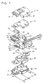
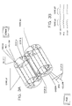
- Fig. 1 shows an exploded view of the improved F-coupler according to the teachings of the present invention.
- the F-coupler can be used in a multi-media communications network such as the one described in the above-referenced U. S. patent 4,885,747.
- the F-coupler includes a common housing formed from bottom cover 10 and top cover 12.
- the top and bottom covers are molded from non-conductive material such as hard plastic.
- the bottom cover 10 is fitted with a pair of upstanding posts 14 and 16 which coact with alignment holes in other components of the F-coupler.
- a pair of latching members coacts with a pair of openings positioned on either side of the top cover 12, one of which is identified by numeral 20, to latch the bottom cover to the top cover.
- a latching mechanism formed by components 22 and 24 coact with a similar mechanism on another connector to hold the resilient tongues (details to be given hereafter) when the F-coupler mates with another hermaphroditic connector.
- the F-coupler further includes a bottom shield assembly 26.
- the bottom shield assembly is fabricated from metal and has a rear portion with upstanding side walls and an opening in the side walls to receive a ferrule 20′ through which a data cable (details to be given hereinafter) is fitted.
- the size of the opening is such that when the ferrule is inserted in the orientation shown in Fig. 1, the ferrule is snugly fitted within the opening.
- a pair of holes are positioned in the front section of the bottom shield assembly. The holes coact with upstanding posts 14 and 16 to position the bottom shield assembly within the bottom cover member 10.
- a housing plug subassembly 28 carries a pair of holes (not shown) in the terminal block section 30 which coact with the mounting posts 14 and 16 to position the housing plug assembly so that the resilient contact tongue is able to coact with like contact tongues on a mating connector.
- a stuffer cap 32 is provided with an extended member which coacts with grooves in the terminal block section 30 to force conductors 32, 34, 36 and 38 into terminal blocks 32′, 34′, 36′ and 38′. It should be noted that the terminal blocks are provided with grooves, not shown, which cut into the plastic cover of the conductors to make contact with the conductor wires.
- the front section of the F-coupler identified by numeral 42 (see also Fig. 5), form a hermaphroditic exit/entry port of the F-coupler.
- This hermaphroditic entry/exit port is substantially similar to the like port described in the connector set forth in Re. 32,760 and USP 5,030,114.
- the rear section of the F-coupler identified by numeral 44 includes insulator 46, F-module 48 and stuffer cap 50.
- the F-module 48 includes the electrical circuit which splits or combines the broadband and baseband signal.
- the insulator 46 insulates the F-module from the bottom shield assembly 26. Details of the F-module 48 will be given subsequently. Suffice it to say at this time that the F-module has a circuit card 52 for mounting the electrical components (to be described subsequently).
- a plurality of barrel connector 54, 56, 58 and 60 are mounted to the card. As will be explained subsequently, the conductors which are carried in cable (Fig.
- a coaxial assembly 62 for carrying broadband signals such as video, etc., is fitted in electrical communications with the component on the circuit card.
- a plurality of conductors 32, 34, 36 and 38 are connected to selected ones of the component.
- conductors 32, 34, 36 and 38 are forced by stuffer cap 32 into barrel terminals 32′, 34′, 36′ and 38′.
- the conductors also form the windings of the transformers (to be described hereinafter).
- the F-coupler has three exit/input terminals formed by coax assembly 62, the resilient contacts 11 (see Fig.
- top shield assembly 40 has downwardly extending side members with openings which coact with locking mechanism (not shown) in the upstanding side walls of the bottom shield assembly 26 to form a closed EMI shield.
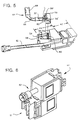
- FIG. 5 there is shown an assembled F-coupler.
- the top shield assembly 40 and a top cover 12 (Fig. 1) are not shown.
- the orientation of the F-coupler shown in Fig. 5 is the reverse of the orientation shown in the disassembled F-coupler shown in Fig. 1.
- the front section 42 of the disassembled F-coupler is pointing towards the left-hand side of the page, whereas in Fig. 5, the front section 42 is pointing towards the right-hand side of the page and the rear section 44 is pointing towards the left edge of the page.
- a cable assembly 64 is connected to the barrel connectors 54, 56, 58 and 60. It should be noted that these barrel connectors are identical to the one shown in Fig. 1 and attached to circuit card 52. The prime (′) designation is used to indicate that they are shown in a different figure.
- the cable assembly 64 is connected to the communications network (not shown) to which the F-coupler is connected.
- cable 64 is the IBM® Data Cable Assembly.
- This data cable assembly comprises four color coded conductors 54′, 56′, 58′ and 60′. Each pair of the color coded conductors are used to transmit signals bidirectionally. Stated another way, one pair of the color-coded conductor transmits signals into the F-coupler and the other pair transmits signals out of the F-coupler.
- the color coded conductors are wrapped in conductive sheath 66 which is also wrapped in a plastic cover 68. Each of the color coded conductors are also wrapped with a plastic cover. In the final assembly shown in Fig. 5, a portion of the outside plastic cover 68 is removed from the cable and the ferrule 20′ (Fig.
- the top shield assembly 40 With the cable assembly 64 firmly in place, the top shield assembly 40 is slid into the bottom shield first, then the top cover assembly 12 and the structure is fitted over the F-Coupler. As stated previously, the holes in the top shield assembly 40 coact with protruding members on the upstanding side of bottom shield assembly 26 to form a closed EMI chamber. Also, the opening 20 in the top cover coacts with the raised member 18 on the bottom cover to form a housing encircling the component of the F-coupler.
- the insulator member 46 is placed in the rear section of bottom shield assembly 26.
- the F-module 48 is placed on top of the insulator 46.
- the orientation of the F-module in the bottom shield assembly 26 is such that the barrel connectors 54, 56, 58 and 60 face the right-hand side of the page, while the coded conductors 32, 34, 36 and 38 face the left-hand side of the page.
- the bottom shield assembly 26 is then placed in the bottom cover 10 so that the holes in the front section of bottom shield assembly is fitted over posts 14 and 16.
- the housing plug assembly 28 is next positioned in the front section 42 of bottom cover 10. As stated previously, alignment holes, not shown, are positioned within the terminal support block 28′.
- the holes coact with posts 14 and 16 to align the housing plug assembly so that the resilient tongues (H, J, K, L) are positioned to coact with similar tongues in a mating connector as described above and shown in U. S. Patents 5,030,114 and Re. 32,760.
- the coded conductors 32, 34, 36 and 38 are fitted into stuffer cap 32 which is forced into support block 28′. As a result, the conductors are forced into contact with the barrel connectors.
- Fig. 6 shows a perspective view of an alternate embodiment of the F-Coupler.
- the alternate embodiment has a broadband entry/exit port to which a coax cable assembly 62′ is connected and could be used to attach broadband devices.
- the alternate embodiment further includes hermaphroditic exit/entry ports 11′ and 11 ⁇ , one of which could be connected to baseband devices via a mating connector and the other could be coupled via a mating connector to a communications network transferring multi-media electrical signals.
- the hermaphroditic exit/entry ports are identical to the one previously described. Therefore, the details of the ports will not be repeated.
- the coax 62′ could be a female F-connector barrel mountdd on PC board 48.
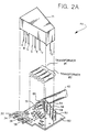
- Fig. 2A shows an exploded view of the F-module 48 of Fig. 1.
- the F-module includes card 52 on which barrel terminals 54, 56, 58 and 60 are mounted. As stated before, each of the barrel terminals has a slot with sharp edges that pierce the insulation of a conductor that is forced into the barrel terminal.
- the card 52 has a plurality of through holes through which conductors are threaded to make contact with electrical conductors or lands (not shown) disposed on the card. Color coded conductors 32, 34, 36 and 38 are threaded through a set of holes on card 52 and make contact with LANs on the underside of the card.
- a plurality of surface mounted electrical circuit components (details to be given subsequently are mounted on the top surface of the card. In Fig.2A, these surface mounted electrical components are shown as rectangular blocks.
- the braid and non-conductive covering on coax assembly 62 is trimmed back as is shown in Fig. 2A and a cable retention half ring 69 is soldered to the braid and anchors the coax assembly to the card.
- the cable retention half ring is in contact via the braid with the PCP or non-conductive portion of the coax assembly which shields the inner conductor 70.
- the inner conductor 70 is forced through a hole on the card to make contact with an appropriate land pattern on the underside of the card 52.
- the transformer shield box 71 which houses the transformer (details to be given hereinafter) is next fitted on an appropriate area of the card.
- the coded wires emanating from the transformer and identified by alphabetical characters A, B, C, D, E, F,....G are threaded through appropriate holes on the card to make contact with selective land patterns on the underside of the card. It should be noted that when the structure is completed, the components including the transformers (to be described subsequently) are totally encircled by the transformer shield box and only coded conductors, coax cable assembly and barrel terminals are shown (see Fig. 1).
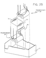
- Fig. 2B shows the shield box and the components which are assembled in the shield box.
- the shield box 71 is fabricated from solid conductive material such as nickel coated brass.
- Two transformers #1 and #2 are positioned in the shield box. Details of the transformers will be given subsequently. Suffice it to say at this point that each of the transformers comprises a pair of cylindrical members with wires emanating from each of the cylindrical members.
- a foil tape 77 is placed around one pair of the transformer and is soldered at solder point 74 and 76 to the bottom and side of shield box 71.
- the items A, B, C,.... represent the wires extending from the transformer.
- a cut-away view shows the positioning of the transformer in the shield box.
- one of the transformers is covered with foil tape 77 and the other is not.
- the foil tape provides a first level of shielding for the signal passing through the covered transformer.
- a second and third level of shielding is provided by the shield box 70 and shield assemblies 26 and 40. Both transformers are fastened to the bottom surface of the shield box.
- an adhesive called Loctite 495 or GE RTV 162 was used.
- the transformers are placed so that the wires are orientated as shown in the cut-away view.
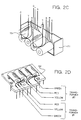
- Fig. 2D the orientation of the transformers relative to circuit card 52 is shown.
- components on the circuit card are removed for clarity.
- the respective wires from the transformer are threaded through holes in the circuit card.
- the holes allows access to printed circuit conductors mounted on the underside of the circuit card.
- Fig. 3A shows a schematic of one of the transformers and how it is wound. Both transformers are identical so the teaching to be given subsequently is applicable to either of the transformers.
- the transformers are fabricated from two ferrite cores, core #1 and core #2, which are cylindrical and are joined together along the respective cylindrical surfaces. Although different methods or adhesives can be used for joining the cores, in one embodiment of this invention, an adhesive called Loctite 495 was used. Even though ferrite cores having different dimensions and/or characteristic can be used, in one embodiment of this invention, a ferrite core, P/N 2664666611 manufactured by Fair-Rite Products Corp. was used with good results.
- Each core is solid and a plurality of elongated holes are bored through the ferrite.
- the holes are parallel and extend along the longitudinal axis of each core.
- six 10 millimeter holes were provided in each of the cores.
- the holes are positioned and orientated as is shown in the figure.
- Each hole extends from the end of the core labeled start and finishes at the other side of the core labeled end.
- each hole is labeled by the same numeral at the start side of the core and at the end side of the core.
- the hole labeled 1 in core 1 has a beginning at the start side of the core and finishes at the end side of the core.
- wires enter hole #1 (core #1 on the start side) and exit the transformer in hole #4 of core #2.
- Fig. 3B shows a schematic of the transformer windings. As can be seen from the schematic the yellow and red wires are continuous through core #1 and #2, while the green wire is non-continuous. This non-continuous feature of the wiring is needed to form the broadband RF coupling for the F-coupler, to the neighboring wire pairs and to effect wide band coupling.
- Fig. 4 shows a circuit diagram for the F-coupler.
- the F-coupler may be considered as having an internal electrical structure identified by numeral 74 and external ports called terminal side and cable side.
- the terminal side of the F-coupler is the side to which a data terminal equipment such as a personal computer, word processor, etc., is attached.
- the terminal side has an A terminal through which data from the cable port of the F-coupler is passed to the terminal.
- the arrow shows the direction of signal travel and a B port to which data (baseband signal) is passed from the terminal into the F-coupler.
- the wires at the A port and B port of the terminal side in Fig. 4 are connected to the barrel terminals in the housing plug assembly 28.
- the output from the mating connector half can be connected to a data terminal equipment.
- this is only one configuration of the F-coupler and it can be used in other ways within the communications network. Still referring to Fig. 4, the green, red, orange and black wires on the cable side of the connector would be the wires which are contained in cable 68, Fig. 5.
- signal paths within the F-coupler 74 is symmetrical. As such, numeral 74A indicates one signal path and numeral 74B indicates the other signal path.
- Signal path 74A carries both the broadband and baseband signal. Both signals co-habitate on the conductor labeled orange and black.
- the broadband signal is extracted or inserted at terminal 79, while the baseband signal is inserted at port B. It should be noted that terminal 79 would be connected to the coax assembly 62 (Fig. 1, Fig. 5).
- Broadband transformer 78, 84 could be either one of the transformers shown and described as transformer #1, #2 in previous figures. Since both broadband and baseband signals are handled by transformer 78, the foil tape 76, Fig. 2B, would shield the transformer. It should be noted that the transformer has multiple levels of shielding and, as a result, any EMI radiation is contained.
- broadband transformer 78 has three windings.
- the windings identified by numerals 78A pass baseband signals and block broadband signals.
- the winding identified by numeral 78B extracts or inserts broadband signals.
- the broadband terminal 79 is connected by circuit means 80 to a reference potential.
- the circuit means 80 includes a capacitor C1 connected in series with resistor R1 which is connected in series with coil L1. Circuit means 80 provides broadband termination for signals within the range of from 50 to 100 megahertz and provides isolation thereafter for signals over 100 megahertz.
- circuit means 80 provides lightening protection to device connected to port 79. As stated before, this device could be one which uses broadband signals such as a television video device, etc.
- the RC time constant of the component in circuit means 80 provide the lightening protection.
- circuit means 82 provides broadband signal termination of the cable for removal of reflections while isolating the data transmission path. Thus, baseband signals can travel through windings 78A without obstruction from the broadband signal.
- Circuit means 82 include resistor R3 connected in series with capacitor C2 and the combination connected in parallel with series connected resistor R4 and capacitor C3. The parallel combination is connected through inductor L2 to a reference potential which could be ground.
- the filtering and/or terminating function which circuit means 82 provides it provides lightening protection to baseband devices connected to the terminal side.
- transmission path 74B includes broadband transformer 84 which allows one type of signal such as baseband signal to pass to the terminal side.
- Resistors R5 and R6 connect the third winding of the broadband transformer 84 to a reference potential.
- the common mode choke windings provide low, medium and high frequency filtering from Khz to Ghz. The operation and theory behind this type of transmission is set forth in the above-referenced U. S. patent 4,885,747 which is incorporated herein and can be used for any purpose.
- the improved F-coupler described herein provides several advantages.
- the multi-hole ferrite core and winding arrangement provides an excellent winding isolation, dimension stability control, balance control and good broadband signal coupling with excellent manufacturing margins.
- the common mode choke windings provide low, medium and high frequency filtering from killohertz to gigahertz, all via this single core arrangement.
- Manufacturing and packaging the F-coupler is made simple because of the structured components used in the package.
- the shielding arrangement which provides three levels of EMI protection also made this F-coupler suitable for use in any environment. The level of shieldings are provided by the copper tape on the transformer cores, the shield can and the shield housing.
- extremely high frequency performance 100 megabit and 800 megahertz
Landscapes
- Engineering & Computer Science (AREA)
- Microelectronics & Electronic Packaging (AREA)
- Details Of Connecting Devices For Male And Female Coupling (AREA)
- Coupling Device And Connection With Printed Circuit (AREA)
- Communication Cables (AREA)
- Small-Scale Networks (AREA)
- Connections By Means Of Piercing Elements, Nuts, Or Screws (AREA)
Claims (14)
- Elektrischer Steckverbinder, umfassend:
einen Multimedia-Anschluß zum Verbinden mit einem Multimedia-Kommunikationsnetz;
einen Breitbandanschluß zum Verbinden mit einer Breitbandeinrichtung;
einen Niederfrequenzanschluß zum Verbinden mit einer Niederfrequenzeinrichtung; und
ein Schaltungsmittel, das zum Verbinden jeden Anschlusses angeordnet ist, wobei das Schaltungsmittel einen ersten Übertragungspfad bereitstellt, der elektrische MultimediaSignale übermittelt;
dadurch gekennzeichnet, daß
ein zweiter Übertragungspfad bereitgestellt wird, der Niederfrequenzsignale übermittelt;
mit dem ersten Übertragungspfad umfassend: einen ersten Übertrager (78), der den Niederfrequenzanschluß mit dem Breitbandanschluß koppelt, ein erstes Schaltungsmittel (82), das ausgewählte Wicklungen (78A) des ersten Übertragers (78) mit einem ersten Bezugsspannungspotential koppelt, um die Breitbandsignale zu begrenzen und die Einrichtungen, die an dem Niederfrequenzanschluß angeschlossen sind, gegen Hochspannungsstöße zu schützen, und ein zweites Schaltungsmittel (80), das ausgewählte Wicklungen (78B) des ersten Übertragers (78) mit einem ersten Bezugsspannungspotential verbindet, um Breitbandsignale innerhalb eines ausgesuchten Bereichs zu begrenzen und um Einrichtungen, die mit dem Breitbandanschluß verbunden sind, gegen Hochspannungsstöße zu schützen, und einem Übertragungsmedium, das das erste Schaltungsmittel (82) mit dem Multimedia-Anschluß verbindet, und
wobei der zweite Übertragungspfad einen zweiten Übertrager (84), der den Niederfrequenzanschluß mit dem Multimedia-Anschluß verbindet, umfaßt. - Elektrischer Steckverbinder nach Anspruch 1, wobei der Multimedia-Anschluß mehrere drahtverbindende Endanschlüsse (54, 56, 58, 60) einschließt.
- Elektrischer Steckverbinder nach Anspruch 1 oder 2, wobei der Niederfrequenzanschluß mehrere Endanschlüsse, die drahtverbindende Abschnitte (54, 56, 58, 60) und federnde Kontaktzungen (H, J, K, L) aufweisen, einschließt.
- Elektrischer Steckverbinder nach einem der Ansprüche 1 bis 3, wobei der Breitbandanschluß eine Koaxialbaugruppe (62) einschließt.
- Elektrischer Steckverbinder nach einem der Ansprüche 1 bis 4, wobei jeder der Übertrager ein Paar zylindrischer Ferritkerne einschließt, die auf ihrem Umfang mit der Verbindungsebene parallel zu der Längsachse von jedem Ferritkern zusammengefügt sind, wobei jeder Ferritkern mehrere Löcher, die sich auf der Länge des Kerns und parallel zu der Längsachse erstrecken, aufweist und mehrere Drähte, die durch die Löcher in den Kernen gefädelt sind.
- Elektrischer Steckverbinder nach einem der Ansprüche 1 bis 5, wobei das erste Schaltungsmittel (82) einen gemeinsamen Knotenpunkt, eine erste in Reihe geschaltete Kondensator- (C2) und Widerstands- (R3) Schaltungsanordnung, die mit dem Knotenpunkt verbunden ist, eine zweite in Reihe geschaltete Kondensator- (C3) und Widerstands- (R4) Schaltung, die mit dem Knotenpunkt verbunden ist und parallel zu der ersten in Reihe geschalteten Kondensator- und Widerstands-Schaltungsanordnung ist und eine Drosselspule (L2), die den gemeinsamen Knotenpunkt mit dem Bezugsspannungspotential verbindet, umfaßt.
- Elektrischer Steckverbinder nach einem der Ansprüche 1 bis 6, wobei das zweite Schaltungsmittel (80) einen Kondensator (C1), einen Widerstand (R1) und eine Drosselspule (L1), die in Reihe geschaltet sind, einschließt.
- Elektrischer Steckverbinder nach einem der Ansprüche 1 bis 7, umfassend:
ein isolierendes Gehäuse (10, 12), das zwei benachbarte Kammern zur Unterbringung der Komponenten aufweist;
einen isolierenden Anschlußträgerblock (30), der innerhalb von einem der beiden benachbarten Kammern befestigt ist;
mehrere leitende Endanschlüsse, die in dem Anschlußträgerblock (30) montiert sind, wobei jeder der mehreren leitenden Endanschlüsse einen Drahtbefestigungsabschnitt (32′, 34′, 36′, 38′) und einen federnden Kontaktabschnitt (H, J, K, L) aufweist;
ein Modul (48), das eine Schaltungsanordnung zum Bereitstellen von Signal-Teilungsfunktionen, Signal-Verknüpfungsfunktionen oder eines Blitzschutzes aufweist, die in der anderen der beiden benachbarten Kammern montiert ist; und
mehrere Leitungen (32, 34, 36, 38), die das Modul (48) mit dem Drahtbefestigungsabschnitt von mehreren leitenden Endanschlüssen (32′, 34′, 36′, 38′) verbinden. - Elektrischer Steckverbinder nach Anspruch 8, weiterhin eine obere (40) und eine untere (26) metallisch leitende Abschirmung umfassend, die innenseitig von dem isolierenden Gehäuse (10, 12) angeordnet ist, um die inneren Komponenten des Steckverbinders zu umhüllen.
- Elektrischer Steckverbinder nach Anspruch 8 oder 9, wobei das Modul (48) eine Karte (52) und mehrere ausgewählte elektrische Komponenten, die auf der Karte (52) befestigt sind, umfaßt;
mehrere drahtaufnehmende Endanschlüsse (54, 56, 58, 60), die auf der Karte befestigt sind, einen ersten Übertrager (78), der einen ersten Satz von Windungen (78A) aufweist, wobei ein Ende mit einem ersten Satz von ausgewählten elektrischen Komponenten (82) auf der Karte (52) verbunden ist und ein anderes Ende des ersten Satzes von Windungen die Karte (52) verläßt, ein erstes elektrisch leitendes Mittel, das ausgewählte drahtaufnehmende Endkontakte mit dem ersten Satz elektrischer Komponenten verbindet, einen zweiten Satz von Windungen (78B), der mit einem zweiten Satz von elektrischen Komponenten (80) auf der Karte (52) verbunden ist; und
ein elektrisch leitendes Mittel, das den zweiten Satz elektrischer Komponenten mit einem Breitband Eingangs/Ausgangsanschluß verbindet. - Elektrischer Steckverbinder nach Anspruch 10, weiterhin einen zweiten Übertrager (84) umfassend, der einen dritten Satz von Windungen aufweist, die mit einem dritten Satz elektrischer Komponenten auf der Karte (52) gekoppelt sind, wobei ein Ende von einem vierten Satz von Windungen mit ausgewählten drahtaufnehmenden Endanschlüssen gekoppelt ist und das andere Ende des vierten Satzes von Windungen die Karte (52) verläßt.
- Elektrischer Steckverbinder nach Anspruch 11, wobei der erste Übertrager (78) und der zweite Übertrager (84) jeweils aus einem Paar von miteinander verbundenen, mehrlöchrigen, zylindrischen Ferritkernen (Fig. 3A); und
mehreren leitenden Drähten, die durch die Löcher von jedem Kern gefädelt sind, gebildet werden. - Elektrischer Steckverbinder nach Anspruch 12, wobei mindestens ein Paar von gewickelten, miteinander verbundenen, mehrlöchrigen, zylindrischen Ferritkernen mit einer Metallfolie (77), die mit der Karte verbunden ist, umhüllt ist (Fig. 2B).
- Elektrischer Steckverbinder nach einem der Ansprüche 10 bis 13, weiterhin ein metallisches Abschirmungsgehäuse (71) umfassend, das mit der Karte (52) verbunden ist, um alle Komponenten auf der Karte (52) zu umhüllen.
Applications Claiming Priority (3)
| Application Number | Priority Date | Filing Date | Title |
|---|---|---|---|
| US07/778,416 US5293298A (en) | 1991-10-16 | 1991-10-16 | Electrical connector |
| PCT/EP1992/002091 WO1993008650A1 (en) | 1991-10-16 | 1992-09-11 | Electrical connector module for multi media, broadband and baseband signal cables |
| US778416 | 1996-12-31 |
Publications (2)
| Publication Number | Publication Date |
|---|---|
| EP0608251A1 EP0608251A1 (de) | 1994-08-03 |
| EP0608251B1 true EP0608251B1 (de) | 1995-07-12 |
Family
ID=25113281
Family Applications (1)
| Application Number | Title | Priority Date | Filing Date |
|---|---|---|---|
| EP92918943A Expired - Lifetime EP0608251B1 (de) | 1991-10-16 | 1992-09-11 | Elektrischer stecker-modul für multi media, breitband- und niederfrequenzkabel |
Country Status (15)
| Country | Link |
|---|---|
| US (1) | US5293298A (de) |
| EP (1) | EP0608251B1 (de) |
| JP (1) | JPH0711971B2 (de) |
| KR (1) | KR950006024B1 (de) |
| AT (1) | ATE125084T1 (de) |
| CZ (1) | CZ282975B6 (de) |
| DE (1) | DE69203458T2 (de) |
| ES (1) | ES2080516T3 (de) |
| HK (1) | HK23996A (de) |
| HU (1) | HU216362B (de) |
| PL (1) | PL169732B1 (de) |
| RU (1) | RU2140706C1 (de) |
| SK (1) | SK40994A3 (de) |
| TW (1) | TW200610B (de) |
| WO (1) | WO1993008650A1 (de) |
Cited By (1)
| Publication number | Priority date | Publication date | Assignee | Title |
|---|---|---|---|---|
| CN101949289A (zh) * | 2010-09-07 | 2011-01-19 | 西安科技大学 | 地层模拟实验用多介质耦合装置 |
Families Citing this family (12)
| Publication number | Priority date | Publication date | Assignee | Title |
|---|---|---|---|---|
| CA2157262C (en) * | 1994-09-08 | 1999-10-26 | Robert Stanton | Surge arrestor for rf devices |
| GB9507574D0 (en) * | 1995-04-12 | 1995-05-31 | Itt Ind Ltd | Electrical connector |
| DE19630202C2 (de) * | 1996-07-26 | 1999-09-23 | Harting Kgaa | Leitungsverzweiger |
| US6422900B1 (en) | 1999-09-15 | 2002-07-23 | Hh Tower Group | Coaxial cable coupling device |
| US6597227B1 (en) * | 2000-01-21 | 2003-07-22 | Atheros Communications, Inc. | System for providing electrostatic discharge protection for high-speed integrated circuits |
| US6413103B1 (en) | 2000-11-28 | 2002-07-02 | Apple Computer, Inc. | Method and apparatus for grounding microcoaxial cables inside a portable computing device |
| US6597256B2 (en) | 2001-01-23 | 2003-07-22 | Adc Telecommunications, Inc. | Multi-circuit signal transformer |
| KR100774748B1 (ko) * | 2006-08-17 | 2007-11-08 | 현대자동차주식회사 | 레지스터 터미널구조 |
| JP5146506B2 (ja) * | 2010-09-14 | 2013-02-20 | 第一精工株式会社 | 電気コネクタ及び電気コネクタ組立体 |
| WO2014158369A1 (en) * | 2013-03-29 | 2014-10-02 | 3M Innovative Properties Company | Modular breakout device for optical and electrical connections |
| CN106953219A (zh) * | 2017-04-28 | 2017-07-14 | 上海未来伙伴机器人有限公司 | 一种输出接头、连接器组合件及飞行机器人 |
| CN113571930A (zh) * | 2020-04-27 | 2021-10-29 | 春源科技(深圳)有限公司 | Rf同轴跳线及其线端连接器与装配方法 |
Family Cites Families (9)
| Publication number | Priority date | Publication date | Assignee | Title |
|---|---|---|---|---|
| US4481641A (en) * | 1982-09-30 | 1984-11-06 | Ford Motor Company | Coaxial cable tap coupler for a data transceiver |
| US4501459A (en) * | 1982-12-22 | 1985-02-26 | Amp Incorporated | Electrical connector |
| DE3326128A1 (de) * | 1983-07-20 | 1985-01-31 | Siemens AG, 1000 Berlin und 8000 München | Anschlussvorrichtung fuer koaxiale kabel |
| US4808843A (en) * | 1985-04-10 | 1989-02-28 | Electric Power Research Institute | Method and means for damping supersynchronous oscillations in an AC power system |
| JPS61269876A (ja) * | 1985-05-23 | 1986-11-29 | 第一電子工業株式会社 | グランド端子をもつ多極コネクタへのテ−プ電線接続方法 |
| US4885747A (en) * | 1988-02-17 | 1989-12-05 | International Business Machines Corp. | Broadband and baseband LAN |
| US4846731A (en) * | 1988-08-03 | 1989-07-11 | Amp Incorporated | Shielded electrical connectors |
| US5053910A (en) * | 1989-10-16 | 1991-10-01 | Perma Power Electronics, Inc. | Surge suppressor for coaxial transmission line |
| US5122921A (en) * | 1990-04-26 | 1992-06-16 | Industrial Communication Engineers, Ltd. | Device for electromagnetic static and voltage suppression |
-
1991
- 1991-10-16 US US07/778,416 patent/US5293298A/en not_active Expired - Fee Related
-
1992
- 1992-04-16 TW TW081102994A patent/TW200610B/zh active
- 1992-07-22 JP JP4195037A patent/JPH0711971B2/ja not_active Expired - Lifetime
- 1992-09-11 WO PCT/EP1992/002091 patent/WO1993008650A1/en active IP Right Grant
- 1992-09-11 RU RU94019980A patent/RU2140706C1/ru active
- 1992-09-11 ES ES92918943T patent/ES2080516T3/es not_active Expired - Lifetime
- 1992-09-11 CZ CZ94816A patent/CZ282975B6/cs not_active IP Right Cessation
- 1992-09-11 EP EP92918943A patent/EP0608251B1/de not_active Expired - Lifetime
- 1992-09-11 HU HU9401055A patent/HU216362B/hu not_active IP Right Cessation
- 1992-09-11 SK SK409-94A patent/SK40994A3/sk unknown
- 1992-09-11 DE DE69203458T patent/DE69203458T2/de not_active Expired - Fee Related
- 1992-09-11 PL PL92303105A patent/PL169732B1/pl unknown
- 1992-09-11 AT AT92918943T patent/ATE125084T1/de not_active IP Right Cessation
- 1992-09-16 KR KR1019920016796A patent/KR950006024B1/ko not_active IP Right Cessation
-
1996
- 1996-02-08 HK HK23996A patent/HK23996A/xx not_active IP Right Cessation
Cited By (2)
| Publication number | Priority date | Publication date | Assignee | Title |
|---|---|---|---|---|
| CN101949289A (zh) * | 2010-09-07 | 2011-01-19 | 西安科技大学 | 地层模拟实验用多介质耦合装置 |
| CN101949289B (zh) * | 2010-09-07 | 2013-04-24 | 西安科技大学 | 地层模拟实验用多介质耦合装置 |
Also Published As
| Publication number | Publication date |
|---|---|
| HU9401055D0 (en) | 1994-07-28 |
| CZ81694A3 (en) | 1994-07-13 |
| ATE125084T1 (de) | 1995-07-15 |
| RU2140706C1 (ru) | 1999-10-27 |
| KR950006024B1 (ko) | 1995-06-07 |
| JPH0689757A (ja) | 1994-03-29 |
| US5293298A (en) | 1994-03-08 |
| KR930009168A (ko) | 1993-05-22 |
| RU94019980A (ru) | 1996-04-20 |
| HK23996A (en) | 1996-02-16 |
| HU216362B (hu) | 1999-06-28 |
| CZ282975B6 (cs) | 1997-11-12 |
| DE69203458D1 (de) | 1995-08-17 |
| DE69203458T2 (de) | 1996-03-07 |
| EP0608251A1 (de) | 1994-08-03 |
| TW200610B (de) | 1993-02-21 |
| JPH0711971B2 (ja) | 1995-02-08 |
| WO1993008650A1 (en) | 1993-04-29 |
| HUT68040A (en) | 1995-05-29 |
| SK40994A3 (en) | 1994-09-07 |
| ES2080516T3 (es) | 1996-02-01 |
| PL169732B1 (pl) | 1996-08-30 |
Similar Documents
| Publication | Publication Date | Title |
|---|---|---|
| US8992248B2 (en) | Modular jack with enhanced port isolation | |
| US6926553B2 (en) | Cable assembly with improved grounding means | |
| EP0901201B1 (de) | Elektrischer Steckverbinder mit verschobener Signalkompensation | |
| EP0608251B1 (de) | Elektrischer stecker-modul für multi media, breitband- und niederfrequenzkabel | |
| US6736681B2 (en) | Communications connector that operates in multiple modes for handling multiple signal types | |
| US7857630B2 (en) | Printed circuit board mounted connector housing shielded cables | |
| US7316584B2 (en) | Matched impedance shielded pair interconnection system for high reliability applications | |
| US8888538B2 (en) | Modular jack with enhanced shielding | |
| JP3446135B2 (ja) | モジュラージャックコネクタ | |
| US20050003707A1 (en) | Cable assembly with internal circuit modules | |
| US11387606B2 (en) | Communication connectors utilizing multiple contact points | |
| US20040266273A1 (en) | Cable assembly with internal circuit modules | |
| US6462637B1 (en) | Electrical connector | |
| US6612857B2 (en) | Electrical connector system and method having optical and/or cooling capability | |
| EP0587367B1 (de) | Anpassungsglied für Fernseh- und Tonsignalübertragung | |
| US20100003861A1 (en) | Plug connector for telecommunications and data technology | |
| US10530106B2 (en) | Modular plug connector with multilayer PCB for very high speed applications | |
| EP0617560A1 (de) | Videoadapter | |
| US20240072497A1 (en) | Perpendicularly mounted network jack with secure connector and magnetics | |
| CN110521069B (zh) | 集成连接器模块以及用于标准化应用的印刷电路卡 | |
| US20030220011A1 (en) | Modular connector for a data communications system enabling near-end crosstalk to be adjusted |
Legal Events
| Date | Code | Title | Description |
|---|---|---|---|
| PUAI | Public reference made under article 153(3) epc to a published international application that has entered the european phase |
Free format text: ORIGINAL CODE: 0009012 |
|
| 17P | Request for examination filed |
Effective date: 19940120 |
|
| AK | Designated contracting states |
Kind code of ref document: A1 Designated state(s): AT BE CH DE ES FR GB IT LI NL SE |
|
| 17Q | First examination report despatched |
Effective date: 19940926 |
|
| GRAA | (expected) grant |
Free format text: ORIGINAL CODE: 0009210 |
|
| AK | Designated contracting states |
Kind code of ref document: B1 Designated state(s): AT BE CH DE ES FR GB IT LI NL SE |
|
| REF | Corresponds to: |
Ref document number: 125084 Country of ref document: AT Date of ref document: 19950715 Kind code of ref document: T |
|
| PGFP | Annual fee paid to national office [announced via postgrant information from national office to epo] |
Ref country code: BE Payment date: 19950726 Year of fee payment: 4 |
|
| REF | Corresponds to: |
Ref document number: 69203458 Country of ref document: DE Date of ref document: 19950817 |
|
| ET | Fr: translation filed | ||
| PGFP | Annual fee paid to national office [announced via postgrant information from national office to epo] |
Ref country code: AT Payment date: 19950825 Year of fee payment: 4 |
|
| PGFP | Annual fee paid to national office [announced via postgrant information from national office to epo] |
Ref country code: ES Payment date: 19950911 Year of fee payment: 4 |
|
| ITF | It: translation for a ep patent filed |
Owner name: IBM - DR. ING. FABRIZIO LETTIERI |
|
| REG | Reference to a national code |
Ref country code: CH Ref legal event code: PK |
|
| RAP2 | Party data changed (patent owner data changed or rights of a patent transferred) |
Owner name: INTERNATIONAL BUSINESS MACHINES CORPORATION Owner name: IBM DEUTSCHLAND GMBH |
|
| PGFP | Annual fee paid to national office [announced via postgrant information from national office to epo] |
Ref country code: CH Payment date: 19951227 Year of fee payment: 4 |
|
| NLT2 | Nl: modifications (of names), taken from the european patent patent bulletin |
Owner name: INTERNATIONAL BUSINESS MACHINES CORPORATION |
|
| REG | Reference to a national code |
Ref country code: ES Ref legal event code: FG2A Ref document number: 2080516 Country of ref document: ES Kind code of ref document: T3 |
|
| RAP2 | Party data changed (patent owner data changed or rights of a patent transferred) |
Owner name: INTERNATIONAL BUSINESS MACHINES CORPORATION |
|
| NLXE | Nl: other communications concerning ep-patents (part 3 heading xe) |
Free format text: PAT.BUL.18/95 PAGE 3127:CORR.:INTERNATIONAL BUSINESS MACHINES CORPORATION |
|
| PLBE | No opposition filed within time limit |
Free format text: ORIGINAL CODE: 0009261 |
|
| STAA | Information on the status of an ep patent application or granted ep patent |
Free format text: STATUS: NO OPPOSITION FILED WITHIN TIME LIMIT |
|
| 26N | No opposition filed | ||
| PG25 | Lapsed in a contracting state [announced via postgrant information from national office to epo] |
Ref country code: AT Effective date: 19960911 |
|
| PG25 | Lapsed in a contracting state [announced via postgrant information from national office to epo] |
Ref country code: ES Free format text: LAPSE BECAUSE OF EXPIRATION OF PROTECTION Effective date: 19960912 |
|
| PG25 | Lapsed in a contracting state [announced via postgrant information from national office to epo] |
Ref country code: LI Effective date: 19960930 Ref country code: CH Effective date: 19960930 Ref country code: BE Effective date: 19960930 |
|
| BERE | Be: lapsed |
Owner name: INTERNATIONAL BUSINESS MACHINES CORP. Effective date: 19960930 |
|
| PG25 | Lapsed in a contracting state [announced via postgrant information from national office to epo] |
Ref country code: NL Effective date: 19970401 |
|
| REG | Reference to a national code |
Ref country code: CH Ref legal event code: PL |
|
| NLV4 | Nl: lapsed or anulled due to non-payment of the annual fee |
Effective date: 19970401 |
|
| REG | Reference to a national code |
Ref country code: ES Ref legal event code: FD2A Effective date: 19990601 |
|
| PGFP | Annual fee paid to national office [announced via postgrant information from national office to epo] |
Ref country code: SE Payment date: 19990809 Year of fee payment: 8 |
|
| PGFP | Annual fee paid to national office [announced via postgrant information from national office to epo] |
Ref country code: GB Payment date: 19990826 Year of fee payment: 8 |
|
| PGFP | Annual fee paid to national office [announced via postgrant information from national office to epo] |
Ref country code: DE Payment date: 19990916 Year of fee payment: 8 |
|
| PGFP | Annual fee paid to national office [announced via postgrant information from national office to epo] |
Ref country code: FR Payment date: 19990917 Year of fee payment: 8 |
|
| PG25 | Lapsed in a contracting state [announced via postgrant information from national office to epo] |
Ref country code: GB Free format text: LAPSE BECAUSE OF NON-PAYMENT OF DUE FEES Effective date: 20000911 |
|
| PG25 | Lapsed in a contracting state [announced via postgrant information from national office to epo] |
Ref country code: SE Free format text: THE PATENT HAS BEEN ANNULLED BY A DECISION OF A NATIONAL AUTHORITY Effective date: 20000929 |
|
| GBPC | Gb: european patent ceased through non-payment of renewal fee |
Effective date: 20000911 |
|
| EUG | Se: european patent has lapsed |
Ref document number: 92918943.9 |
|
| PG25 | Lapsed in a contracting state [announced via postgrant information from national office to epo] |
Ref country code: FR Free format text: LAPSE BECAUSE OF NON-PAYMENT OF DUE FEES Effective date: 20010531 |
|
| PG25 | Lapsed in a contracting state [announced via postgrant information from national office to epo] |
Ref country code: DE Free format text: LAPSE BECAUSE OF NON-PAYMENT OF DUE FEES Effective date: 20010601 |
|
| REG | Reference to a national code |
Ref country code: FR Ref legal event code: ST |
|
| PG25 | Lapsed in a contracting state [announced via postgrant information from national office to epo] |
Ref country code: IT Free format text: LAPSE BECAUSE OF NON-PAYMENT OF DUE FEES;WARNING: LAPSES OF ITALIAN PATENTS WITH EFFECTIVE DATE BEFORE 2007 MAY HAVE OCCURRED AT ANY TIME BEFORE 2007. THE CORRECT EFFECTIVE DATE MAY BE DIFFERENT FROM THE ONE RECORDED. Effective date: 20050911 |