EP0604975B1 - Image-forming apparatus - Google Patents
Image-forming apparatus Download PDFInfo
- Publication number
- EP0604975B1 EP0604975B1 EP93121006A EP93121006A EP0604975B1 EP 0604975 B1 EP0604975 B1 EP 0604975B1 EP 93121006 A EP93121006 A EP 93121006A EP 93121006 A EP93121006 A EP 93121006A EP 0604975 B1 EP0604975 B1 EP 0604975B1
- Authority
- EP
- European Patent Office
- Prior art keywords
- image
- electron
- voltage
- electrodes
- forming member
- Prior art date
- Legal status (The legal status is an assumption and is not a legal conclusion. Google has not performed a legal analysis and makes no representation as to the accuracy of the status listed.)
- Expired - Lifetime
Links
Images


Classifications
-
- H—ELECTRICITY
- H01—ELECTRIC ELEMENTS
- H01J—ELECTRIC DISCHARGE TUBES OR DISCHARGE LAMPS
- H01J1/00—Details of electrodes, of magnetic control means, of screens, or of the mounting or spacing thereof, common to two or more basic types of discharge tubes or lamps
- H01J1/02—Main electrodes
- H01J1/30—Cold cathodes, e.g. field-emissive cathode
- H01J1/316—Cold cathodes, e.g. field-emissive cathode having an electric field parallel to the surface, e.g. thin film cathodes
-
- H—ELECTRICITY
- H01—ELECTRIC ELEMENTS
- H01J—ELECTRIC DISCHARGE TUBES OR DISCHARGE LAMPS
- H01J31/00—Cathode ray tubes; Electron beam tubes
- H01J31/08—Cathode ray tubes; Electron beam tubes having a screen on or from which an image or pattern is formed, picked up, converted, or stored
- H01J31/10—Image or pattern display tubes, i.e. having electrical input and optical output; Flying-spot tubes for scanning purposes
- H01J31/12—Image or pattern display tubes, i.e. having electrical input and optical output; Flying-spot tubes for scanning purposes with luminescent screen
- H01J31/123—Flat display tubes
- H01J31/125—Flat display tubes provided with control means permitting the electron beam to reach selected parts of the screen, e.g. digital selection
- H01J31/127—Flat display tubes provided with control means permitting the electron beam to reach selected parts of the screen, e.g. digital selection using large area or array sources, i.e. essentially a source for each pixel group
-
- H—ELECTRICITY
- H01—ELECTRIC ELEMENTS
- H01J—ELECTRIC DISCHARGE TUBES OR DISCHARGE LAMPS
- H01J2201/00—Electrodes common to discharge tubes
- H01J2201/30—Cold cathodes
- H01J2201/316—Cold cathodes having an electric field parallel to the surface thereof, e.g. thin film cathodes
- H01J2201/3165—Surface conduction emission type cathodes
Definitions
- the present invention relates to methods for producing an image forming apparatus.
- the invention relates further to the use and a method of driving of an image forming apparatus produced by said method.
- EP-A-0 312 007 discloses an electron beam emitting device comprising a surface conduction type of thin film device having an electron emitting area and at least a pair of electrodes for passing current through the electron emitting area, and a voltage applying means for applying independently on each of said electrodes, said voltage applying means being a means for applying voltage on each electrode so that each of the electrodes may become higher or lower in potential relative to the other electrode.
- EP-A-0 404 022 describes a flat configuration image display apparatus and a manufacturing method thereof, comprising an electron beam generator equipped with cold cathodes for generating a plurality of electron beams in response to image signals fed from an image signal supplying circuit, electron beam control electrodes for selectively energizing the cold cathodes of the electron beam generator in accordance with a scanning line selection signal.
- the electron control electrodes are divided into a plurality of groups each of which are responsive to the scanning line selection signal through a common bus.
- Flat panel display apparatus practically used includes liquid crystal display apparatuss, EL display apparatuss, and plasma display panels. These are not satisfactory for image displaying in view of the visual field angle, displayed colors, luminance, and so forth.
- the flat panel display apparatuss are inferior to cathode ray tubes (CRT) in the displaying characteristics, and cannot be used as a substitute for the CRT at present.
- CTR cathode ray tubes
- Japanese Patent Appln. Laid-Open Nos. 58-1956 and 60-225342 disclose flat panel image forming device which comprise a plurality of electron source arranged in one plane and fluorescent targets counterposed thereto for receiving an electron beam respectively from the electron sources.
- Fig. 11 illustrates schematically a apparatus constituting a conventional display apparatus.
- the apparatus comprises a glass substrate 71, supports 72, electron-emitting regions 73, wiring electrodes 74, electron passage holes 14, modulation electrodes 15, a glass plate 5, a transparent electrode 6, and an image-forming member 7.
- the image-forming member is made of a material which emits light, changes its color, become electrically charged, or is denatured on collision of electrons, e.g., a fluorescent material, a resist material, etc.
- the glass plate 5, the transparent electrode 6 and the image-forming member 7 constitute a face plate 8.
- the numeral 9 denotes luminous spots of the fluorescent member.
- the electron-emitting region 73 is formed by a thin film technique and has a hollow structure without contacting with the glass plate 71.
- the wiring electrode may be made of the same material as the electron-emitting region or a different material therefrom, and has generally a high melting point and a low electric resistance.
- the support 72 may be made of an insulating material or of an electroconductive material.
- a voltage is applied to the wiring electrodes to emit electrons from the electron-emitting regions 73, the electrons are derived by applying a voltage to the modulation electrodes 15 which conduct modulation in accordance with information signals, and the derived electrons are accelerated to collide against the fluorescent member 7.
- the wiring electrodes and the modulation electrodes are arranged in an X-Y matrix to display an image on the image forming member 7.
- thermoelectron source which uses a thermoelectron source, has disadvantages of (1) high power consumption, (2) difficulty in display of a large quantity of images because of low modulation speed, and (3) difficulty in display of large area because of variation among the devices.
- thermoelectron source An image-forming apparatus having arrangement of surface conduction electron-emitting devices in place of the thermoelectron source is expected to offset the above disadvantages.
- the surface conduction electron-emitting device emits electrons with a simple structure, and is exemplified by a cold cathode device disclosed by M.I. Elinson, et al. (Radio Eng. Electron Phys. Vol. 10, pp. 1290-1296 (1965)). This device utilizes the phenomenon that electrons are emitted from a thin film of small area formed on a substrate on application of electric current in a direction parallel to the film face.
- the surface conduction electron-emitting device in addition to the above-mentioned one disclosed by Elinson et al. employing SnO 2 (Sn) thin film, includes the one employing an Au thin film (G. Dittmer: “Thin Solid Films", Vol. 9, p. 317 (1972)), the one employing an ITO thin film (M. Hartwell, and C.G. Fonstad: "IEEE Trans. ED Conf.”, p. 519 (1975)), the one employing a carbon thin film (H. Araki et al.: “Sinkuu (Vacuum)", Vol. 26, No. 1, p. 22 (1983)), and so forth.
- Fig. 12 illustrates a construction of an image forming device employing such a surface conduction electron-emitting device for use for image forming apparatus.
- the device comprises an insulating substrate 1, device electrodes 2, 3, and electron-emitting regions 4.
- an image is formed by application of a voltage through device wiring electrodes 81 between the device electrodes 2, 3 to emit electrons and by control of the intensity of the electron beam projected to a fluorescent member 7 by applying a voltage to modulation electrodes 15 corresponding to information signals.
- thermoelectron sources As well known, when a planar target is placed in opposition to a thermoelectron source and electrons are accelerated by application of a positive voltage to the target, the electron beam collides against the target in a form corresponding nearly to the shape of the electron source. Accordingly, in an image-forming apparatus employing thermoelectron sources as shown in Fig. 11, the shape of the electron beam spot formed on the image-forming member can readily be controlled by suitably designing the shape of the electron sources.
- the image-forming apparatus employing thermoelectron sources has disadvantages mentioned above and cannot meet satisfactorily the demand for high picture qualities and a large picture size.
- the surface conduction electron-emitting device which has the aforementioned advantages is expected to enable the construction of image-forming apparatus which satisfies the above demands.
- an voltage is applied to the electrodes connected to a thin film in the direction parallel to the substrate surface to flow an electric current in a direction parallel to the thin film formed on the substrate, whereby electrons are emitted.
- the emitted electrons are affected by the electric field generated by the applied voltage.
- the electrons are deflected toward the higher potential electrode, or the trajectory of electrons is distorted before the electrons reach the face of the image-forming member. Therefore, the shape and the size of the electron beam spot on the image-forming member cannot readily be predicted.
- the shape of the electron beam spot on the image-forming member will be deformed or distorted, so that a spot in an axial symmetry, like a circle, cannot readily be obtained.
- An object of the present invention is to provide a method of producing an image-forming apparatus which is capable of forming a sharp image with improved symmetry of the shape of the electron beam spot with improved image resolution without deformation.
- Another object of the present invention is to provide a method of producing an image forming apparatus having surface conduction electron-emitting devices or similar devices which emits electrons by applying voltage between planar electrode pairs on a substrate, in which the size of the electron beam spot can be determined by the voltage applied to the device, the electron acceleration voltage, the distance between the device and the image-forming member, and other factors.
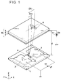
- Fig. 1 is a schematic perspective view illustrating construction of a picture device of an image forming apparatus unit employing surface conduction electron-emitting device as an electron source and also illustrating electron trajectory therein.
- the surface conduction electron-emitting device comprises an insulating substrate 1, a high potential device electrode 2, a low potential device electrode 3, and an electron-emitting region 4.
- the two electrodes 2, 3 are formed with a narrow gap on the substrate 1, and the electron-emitting region 4 constituted of a thin film is formed at the gap.
- the face plate 8 is placed in opposition to the device substrate to construct the image forming apparatus.
- the face plate 8 is constituted of a glass plate 5, a transparent electrode 6, an image forming member 7 (a fluorescent member in this example), and is placed above the insulating substrate 1 at a distance "d".
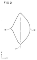
- Fig. 2 is an enlarged schematic diagram of the luminous spot 9 observed on the fluorescent member in the apparatus shown in Fig. 1.
- the numeral 17 denotes a center axis.
- the entire luminous spot is observed to spread in the direction of the voltage application in the device electrodes (X direction in the drawing) and in the direction perpendicular thereto (Y direction in the drawing).
- the electrons emitted in a direction tilting to the high potential electrode side reach the tip portion 18 of the luminous spot
- the electrons emitted in a direction tilting to the low potential electrode side reach the tail portion 19 of the luminous spot, thus the spread of the spot in the X direction being caused by emission of electrons with emission angle distribution relative to the substrate face.
- the amount of electrons emitted to the low potential electrode direction is much less because the luminance is lower at the tail portion than in other portions.
- the luminous spot 9 deviates from the direction perpendicular to the electron-emitting region 4 to the plus X direction, i.e., to the side of high potential device electrode 2, according to experiments conducted by the inventors of the present invention.
- This is probably due to the fact that, in the field above the surface conduction electron-emitting device, the equipotential surfaces are not parallel to the image-forming member 7 in the vicinity of the electron-emitting region, and the emitted electrons are not only accelerated by the acceleration voltage V a in Z direction in the drawing but also accelerated toward the high potential device electrode. That is, the electrons, immediately after they are emitted, are unavoidably subjected to deflecting action of the applied voltage V f which is necessary for electron emission.
- C (eV) is the velocity component of the electron in X direction after the acceleration in the X direction in the vicinity of the electron-emitting region
- C is a constant which depends on the voltage V f applied to the device.
- the constant C as a function of V f is represented by C(V f ) (unit: eV).
- Equation (2) represents the distance of deviation of the electron which is emitted from the electron-emitting region at an initial velocity of zero in X direction and is accelerated by the voltage Vf applied to the device to gain a velocity of C (eV) in X direction in the vicinity of the electron-emitting region.
- the electrons are considered to be emitted at a certain initial velocity in all directions.
- the initial velocity to be v 0 (eV)
- the initial velocity v 0 is also a constant which depends on the voltage energy V f applied to the electron-emitting region.
- the spot size in the direction perpendicular to the voltage application direction in the electron-emitting device is considered.
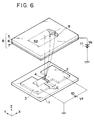
- the electron beam is considered to be emitted at the initial velocity of v 0 also in the direction perpendicular to the voltage application direction in the electron-emitting device (in Y direction in Fig. 6).
- the electron beam is accelerated only little in Y direction after the emission.
- the inventors of the present invention considered the relations of electron beams emitted from a plurality of electron-emitting regions on the image-forming member on the basis of the above Equations.
- the emitted electrons reach the image-forming member in an asymmetric shape relative to the X axis as shown in Fig. 2 owing to the distortion of electric field in the vicinity of the device electrodes (Fig. 3), the effect of the electrode edge, and other factors.
- the distortion and the asymmetry of the spot shape will decrease the resolution of the image, causing low decipherability of letters and unsharpness of animations.
- the luminous spot is in a shape asymmetric to the X axis, but the deviations of the tip portion and the tail portion are known from Equations (5) and (6). Accordingly, it has been found by the inventors of the present invention that a plurality of electron-emitting regions formed at a distance D on both sides of the high potential electrode of the device electrodes gives a luminous spot in satisfactory symmetric shape by the electron beams falling onto one spot on the image-forming member.
- FIG. 1 is a schematic perspective view illustrating a construction of one picture device of the image forming apparatus of the present invention.
- Fig. 2 is a magnified drawing of one luminous spot.
- an insulating substrate 1 made of a glass plate was washed sufficiently.
- a high potential device electrode 2 and a low potential device electrode 3 were formed from nickel and chromium respectively in a thickness of 0.1 ⁇ m by conventional vapor deposition, photolithography, and etching.
- the device electrodes may be made of any material provided that the electric resistance thereof is sufficiently low.
- the formed device electrodes had an electrode gap of 2 ⁇ m wide. Generally, the gap is preferably in a width of from 0.1 ⁇ m to 10 ⁇ m.
- a fine particle film was formed as an electron-emitting region 4 at the gap portion by a gas deposition method.
- palladium was employed as the material for the fine particles.
- Another material may be used therefor, the preferred material including metals such as Ag and Au; and oxides such as SnO 2 and In 2 O 3 , but are not limited thereto.
- the diameter of the Pd particles formed was about 10 nm (100 ⁇ ). However, the diameter is not limited thereto.
- the fine particle film having desired properties may be formed, for example, by application of a dispersion of an organic metal and subsequent heat treatment.
- the length L of the electron-emitting region was 150 ⁇ m in this Example.
- a face plate 8 was prepared by vapor-depositing a transparent electrode 6 of ITO on the one face of the glass plate 5, and thereon providing an image-forming member (a fluorescent member 7 in this Example) by a printing method or a precipitation method.
- the face plate 8 was fixed by a supporting frame (not shown in the drawing) at a distance of 3 mm above the substrate 1 having electron-emitting devices to produce an image-forming apparatus of the present invention.
- the spot size S 1 in X direction was found to be about 260 ⁇ m, which agrees with the calculated value from Equation (16).
- FIG. 4 is a schematic perspective view illustrating a construction of one picture device of the image forming apparatus of the present invention.
- Fig. 4 is a magnified sectional view of the electron-emitting device of Fig. 4 taken along the plane A-A'.
- an insulating substrate 1 made of a glass plate was washed sufficiently.
- a high potential device electrode 2 and a low potential device electrodes 3a, 3b were formed from nickel and chromium respectively in a thickness of 0.1 ⁇ m by conventional vapor deposition, photolithography, and etching.
- the device electrodes 2, 3a, 3b may be made of any material provided that the electric resistance thereof is sufficiently low.
- the device electrodes 2, 3a, 3b were made to have two gaps of 2 ⁇ m wide (G in Fig. 5). Generally, the gaps are preferably in a width of from 0.1 ⁇ m to 10 ⁇ m.
- fine particle films were formed as electron-emitting regions 4a, 4b at the gap portions by a gas deposition method.
- palladium was employed as the material for the fine particles.
- Another material may be used therefor, the preferred material including metals such as Ag and Au; and oxides such as SnO 2 and In 2 O 3 , but are not limited thereto.
- the diameter of the Pd particles formed was about 10 nm (100 ⁇ ). However, the diameter is not limited thereto.
- the fine particle film having desired properties may be formed, for example, by application of a dispersion of an organic metal and subsequent heat treatment.
- the length of the electron-emitting region in Y direction was 150 ⁇ m
- the width of the high potential device electrode 2 (D in Fig. 5) was 400 ⁇ m in this Example.
- a face plate 8 was prepared by vapor-depositing a transparent electrode 6 of ITO on the one face of the glass plate 5, and thereon providing an image-forming member (a fluorescent member 7 in this Example) by a printing method or a precipitation method.
- the face plate 8 was fixed by a supporting frame (not shown in the drawing) at a distance of 3.0 mm above the substrate 1 having electron-emitting devices to produce an image-forming apparatus of the present invention.
- the deviations of the electrons reaching the fluorescent member 7 from the electron-emitting region 4a in plus X direction, and from the electron-emitting region 4b in X minus direction are within the range between the maximum value of ⁇ X 1 and the minimum value of ⁇ X 2 calculated according to the aforementioned approximate Equations (5) and (6).
- the formed spot is in a symmetrical shape, and distinctness and sharpness of the displayed image are improved when a plurality of electron-emitting devices is provided at a distance D satisfying Equation (13) on the both sides of the high potential electrode.
- the size of the luminous spot in Y direction was measured with the image-forming apparatus having a picture device shown in Fig. 6.
- the apparatus was produced in the same manner as in Example 1.
- the face plate 8 was placed 3 mm above the substrate 1 with a supporting frame (not shown in the drawing).
- a driving voltage V f of 14 V was applied between the device electrodes so as to give high potential to the device electrode 2 by the device driving power source 10 to emit electrons from the electron emitting region 4, and an accelerating voltage of 6 kV was applied to the fluorescent member 7 by the electron beam accelerating power source 11 through the transparent electrode 6.
- the electron-emitting region 4 had a length L of 150 ⁇ m in Y direction.
- the size S 2 of the luminous spot 9 in Y direction on the fluorescent member on the image forming member was measured visually with a microscope at a magnification of about 50 ⁇ .
- the size S 2 was found to be about 650 ⁇ m.
- the experimentally measured size agrees satisfactorily with this calculated value.
- Fig. 7 is a perspective view of a portion of an image-forming apparatus of this Example, in which a number of electron emitting devices are arranged in Y direction.
- Example 2 The apparatus was produced in the same way as in Example 1. Therefore the method of production thereof is not described here.
- a driving voltage V f of 14 V was applied between the device electrodes so as to give high potential to the device electrode 2 by the device driving power source 10 to emit electrons from the electron emitting region 4, and an accelerating voltage of 6 kV was applied to the fluorescent member 7 by the electron beam accelerating power source 11 through the transparent electrode 6.
- the distance d between the inside face of the face plate 8 and the substrate 1 having the electron-emitting devices was 3 mm.
- the luminous spot size S 2 in Y direction is calculated to be at least 614 ⁇ m.
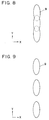
- the arrangement pitch of the devices was 500 ⁇ m. Therefore, the luminous spots on the fluorescent member overlapped with each other in the Y direction as shown in Fig. 8, so that the spots looked like a continuous line, making displayed image continuous.
- this forming apparatus is particularly suitable for display of animations.
- An image forming apparatus was produced in the same manner as in Example 4 except that the electron-emitting devices were arranged at an arrangement pitch P of 800 ⁇ m in perpendicular to the voltage application direction, namely in Y direction.
- the arrangement pitch P of the devices in Y direction is larger than the maximum spot size of 671 ⁇ m in the Y direction. Therefore, the luminous spots on the fluorescent member was observed to be completely separated, so that the formed image was distinct and sharp, being particularly suitable for forming letters or the like.
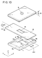
- An image-forming apparatus was produced by the method of the present invention, having a construction as shown in Fig. 10.
- the surface conduction electron-emitting devices were formed in the same manner as in Example 2.
- a modulation electrode 15 was placed between the substrate 1 and the face plate 8.
- Voltage V G was applied to the modulation electrode 15 by a power source 16 in correspondence with information signals to control the quantity of the electron beam projected from the electron-emitting device to the fluorescent member 7.
- the modulation electrode 15 controls the electron beam to be projected to the fluorescence member 7 (ON state) or to be cut off (OFF state). Therefore, in the image-forming apparatus of this Example, the shape of the electron beams or of the luminous spots is not affected by the variation of the modulation voltage V G , and the luminous spots are not distorted or not made non-uniform, unlike the case in which shape of the electron beams (or of luminous spots) is controlled by the modulation voltage V G .
- the present invention relates to a image-forming apparatus employing surface conduction electron-emitting devices or employing electron-emitting devices in which electrons are emitted by application of voltage between electrodes formed in a plane shape on s substrate.
- the size of the electron beam spots can be calculated as a function of the voltage applied to the devices, acceleration voltage, and a distance between the devices and the image-forming member according to the present invention.
- the image-forming apparatuss can readily be designed to be suitable for application fields such as animation application fields and letter forming field, and image-forming apparatuss can be produced which is capable of giving high quality of display.
- the beam spots is improved to be symmetric and non-distorted in shape, thereby an image being obtained with improved resolution, distinctness, and sharpness advantageously.
- the image-forming apparatus of the present invention will possibly be useful widely in public and industrial application fields such as high-definition TV picture tubes, computer terminals, large-picture home theaters, TV conference systems, TV telephone systems, and so forth.
Abstract
Description
- The present invention relates to methods for producing an image forming apparatus. The invention relates further to the use and a method of driving of an image forming apparatus produced by said method.
- EP-A-0 312 007 discloses an electron beam emitting device comprising a surface conduction type of thin film device having an electron emitting area and at least a pair of electrodes for passing current through the electron emitting area, and a voltage applying means for applying independently on each of said electrodes, said voltage applying means being a means for applying voltage on each electrode so that each of the electrodes may become higher or lower in potential relative to the other electrode.
- EP-A-0 404 022 describes a flat configuration image display apparatus and a manufacturing method thereof, comprising an electron beam generator equipped with cold cathodes for generating a plurality of electron beams in response to image signals fed from an image signal supplying circuit, electron beam control electrodes for selectively energizing the cold cathodes of the electron beam generator in accordance with a scanning line selection signal. The electron control electrodes are divided into a plurality of groups each of which are responsive to the scanning line selection signal through a common bus.
- Flat panel display apparatus practically used includes liquid crystal display apparatuss, EL display apparatuss, and plasma display panels. These are not satisfactory for image displaying in view of the visual field angle, displayed colors, luminance, and so forth. In particular, the flat panel display apparatuss are inferior to cathode ray tubes (CRT) in the displaying characteristics, and cannot be used as a substitute for the CRT at present.
- However, with the progress of information processing by computers, and with the improvement in image quality in TV broadcasting, demands are increasing for the flat panel display apparatus of high definition and large display size.
- To meet the demands, Japanese Patent Appln. Laid-Open Nos. 58-1956 and 60-225342 disclose flat panel image forming device which comprise a plurality of electron source arranged in one plane and fluorescent targets counterposed thereto for receiving an electron beam respectively from the electron sources.
- These electron beam display apparatuss have a structure shown below. Fig. 11 illustrates schematically a apparatus constituting a conventional display apparatus. The apparatus comprises a glass substrate 71, supports 72, electron-emitting regions 73, wiring electrodes 74, electron passage holes 14, modulation electrodes 15, a glass plate 5, a transparent electrode 6, and an image-forming member 7. The image-forming member is made of a material which emits light, changes its color, become electrically charged, or is denatured on collision of electrons, e.g., a fluorescent material, a resist material, etc. The glass plate 5, the transparent electrode 6 and the image-forming member 7 constitute a face plate 8. The numeral 9 denotes luminous spots of the fluorescent member. The electron-emitting region 73 is formed by a thin film technique and has a hollow structure without contacting with the glass plate 71. The wiring electrode may be made of the same material as the electron-emitting region or a different material therefrom, and has generally a high melting point and a low electric resistance. The support 72 may be made of an insulating material or of an electroconductive material.
- In such an electron beam display apparatus, a voltage is applied to the wiring electrodes to emit electrons from the electron-emitting regions 73, the electrons are derived by applying a voltage to the modulation electrodes 15 which conduct modulation in accordance with information signals, and the derived electrons are accelerated to collide against the fluorescent member 7. The wiring electrodes and the modulation electrodes are arranged in an X-Y matrix to display an image on the image forming member 7.
- The aforementioned electron beam displaying apparatus, which uses a thermoelectron source, has disadvantages of (1) high power consumption, (2) difficulty in display of a large quantity of images because of low modulation speed, and (3) difficulty in display of large area because of variation among the devices.
- An image-forming apparatus having arrangement of surface conduction electron-emitting devices in place of the thermoelectron source is expected to offset the above disadvantages.
- The surface conduction electron-emitting device emits electrons with a simple structure, and is exemplified by a cold cathode device disclosed by M.I. Elinson, et al. (Radio Eng. Electron Phys. Vol. 10, pp. 1290-1296 (1965)). This device utilizes the phenomenon that electrons are emitted from a thin film of small area formed on a substrate on application of electric current in a direction parallel to the film face.
- The surface conduction electron-emitting device, in addition to the above-mentioned one disclosed by Elinson et al. employing SnO2(Sn) thin film, includes the one employing an Au thin film (G. Dittmer: "Thin Solid Films", Vol. 9, p. 317 (1972)), the one employing an ITO thin film (M. Hartwell, and C.G. Fonstad: "IEEE Trans. ED Conf.", p. 519 (1975)), the one employing a carbon thin film (H. Araki et al.: "Sinkuu (Vacuum)", Vol. 26, No. 1, p. 22 (1983)), and so forth.
- These surface conduction electron-emitting devices have advantages of (1) high electron emission efficiency, (2) simple structure and ease of production, (3) possibility of arrangement of a large number of devices on one substrate, (4) high response speed, and so forth, and are promising in many application fields.
- Fig. 12 illustrates a construction of an image forming device employing such a surface conduction electron-emitting device for use for image forming apparatus. The device comprises an insulating substrate 1, device electrodes 2, 3, and electron-emitting regions 4.
- In this image-forming apparatus employing the surface conduction electron-emitting devices also, an image is formed by application of a voltage through device wiring electrodes 81 between the device electrodes 2, 3 to emit electrons and by control of the intensity of the electron beam projected to a fluorescent member 7 by applying a voltage to modulation electrodes 15 corresponding to information signals.
- As well known, when a planar target is placed in opposition to a thermoelectron source and electrons are accelerated by application of a positive voltage to the target, the electron beam collides against the target in a form corresponding nearly to the shape of the electron source. Accordingly, in an image-forming apparatus employing thermoelectron sources as shown in Fig. 11, the shape of the electron beam spot formed on the image-forming member can readily be controlled by suitably designing the shape of the electron sources. However, the image-forming apparatus employing thermoelectron sources has disadvantages mentioned above and cannot meet satisfactorily the demand for high picture qualities and a large picture size.
- On the other hand, the surface conduction electron-emitting device which has the aforementioned advantages is expected to enable the construction of image-forming apparatus which satisfies the above demands. In the surface conduction electron-emitting device, an voltage is applied to the electrodes connected to a thin film in the direction parallel to the substrate surface to flow an electric current in a direction parallel to the thin film formed on the substrate, whereby electrons are emitted. The emitted electrons are affected by the electric field generated by the applied voltage. Thereby the electrons are deflected toward the higher potential electrode, or the trajectory of electrons is distorted before the electrons reach the face of the image-forming member. Therefore, the shape and the size of the electron beam spot on the image-forming member cannot readily be predicted. It is extremely difficult to decide the application voltage (Vf) to the electron-emitting device, the electron beam acceleration voltage (Va) applied to the image-forming member, the distance (d) between the substrate and the image-forming member, and so forth.
- Since the electron beam is subjected to the aforementioned deflecting action during projection onto the image-forming member, the shape of the electron beam spot on the image-forming member will be deformed or distorted, so that a spot in an axial symmetry, like a circle, cannot readily be obtained.
- An object of the present invention is to provide a method of producing an image-forming apparatus which is capable of forming a sharp image with improved symmetry of the shape of the electron beam spot with improved image resolution without deformation.
- Another object of the present invention is to provide a method of producing an image forming apparatus having surface conduction electron-emitting devices or similar devices which emits electrons by applying voltage between planar electrode pairs on a substrate, in which the size of the electron beam spot can be determined by the voltage applied to the device, the electron acceleration voltage, the distance between the device and the image-forming member, and other factors.
- These objects are achieved by methods according to the independent claims.
- The invention is further developed by the features mentioned in the dependent claims.
- Fig. 1 is a schematic perspective view illustrating a picture device construction of an image-forming apparatus in Example 1 produced by the method of the present invention.
- Fig. 2 illustrates the shape of the luminous spot observed in Example 1.
- Fig. 3 illustrates the projection state of an electron beam in an image-forming apparatus employing an surface conduction electron-emitting device.
- Fig. 4 is a perspective view illustrating constitution of a picture device of an image-forming apparatus in Example 2 produced by the method of the present invention.
- Fig. 5 is an enlarged sectional view of the electron emitting device taken along the plane A-A' in Fig. 4.
- Fig. 6 is a perspective view for explaining an image-forming apparatus in Example 3 produced by the method of the present invention.
- Fig. 7 is a perspective view illustrating an picture device construction of an image-forming apparatus in Example 4 produced by the method of the present invention.
- Fig. 8 illustrates a shape of a luminous spot observed in image forming apparatus in Example 4 produced by the method of the present invention.
- Fig. 9 illustrates a shape of a luminous spot observed in image forming apparatus in Example 5 produced by the method of the present invention.
- Fig. 10 is a perspective view illustrating constitution of a picture device of an image forming apparatus in Example 6 produced by the method of the present invention.
- Fig. 11 illustrates a conventional image-forming apparatus employing thermoelectron sources.
- Fig. 12 illustrates a conventional image-forming apparatus employing surface conduction type electron-emitting devices.
-
- The technical background and effects of the present invention are described below in detail by reference to drawings.
- Fig. 1 is a schematic perspective view illustrating construction of a picture device of an image forming apparatus unit employing surface conduction electron-emitting device as an electron source and also illustrating electron trajectory therein.
- In Fig. 1, the surface conduction electron-emitting device comprises an insulating substrate 1, a high potential device electrode 2, a low potential device electrode 3, and an electron-emitting region 4. The two electrodes 2, 3 are formed with a narrow gap on the substrate 1, and the electron-emitting region 4 constituted of a thin film is formed at the gap. The face plate 8 is placed in opposition to the device substrate to construct the image forming apparatus. The face plate 8 is constituted of a glass plate 5, a transparent electrode 6, an image forming member 7 (a fluorescent member in this example), and is placed above the insulating substrate 1 at a distance "d".
- In the above constitution, when a voltage Vf is applied by an device-driving power source 10 between the device electrodes 2, 3, electrons are emitted from the electron-emitting region 4. The emitted electrons are accelerated by acceleration voltage Va applied by an electron beam-accelerating power source 11 through the transparent electrode 6 to the fluorescent member 7, and collide against the fluorescent member 7 to form a luminous spot 9 on the face plate 8.
- Fig. 2 is an enlarged schematic diagram of the luminous spot 9 observed on the fluorescent member in the apparatus shown in Fig. 1. The numeral 17 denotes a center axis.
- As shown in Fig. 2, the entire luminous spot is observed to spread in the direction of the voltage application in the device electrodes (X direction in the drawing) and in the direction perpendicular thereto (Y direction in the drawing).
- The reason why such a luminous spot is formed or why the electron beam reaches the image-forming member with a certain spread is not clear, since the electron-emission mechanism of the surface conduction electron-emitting device is not completely elucidated. It is presumed by the inventor of the present invention that electrons are emitted at a certain initial velocity in all directions, on the basis of many experiments.
- It is also presumed by the inventor of the present invention that the electrons emitted in a direction tilting to the high potential electrode side (plus X direction in the drawing) reach the tip portion 18 of the luminous spot, and the electrons emitted in a direction tilting to the low potential electrode side (minus X direction in the drawing) reach the tail portion 19 of the luminous spot, thus the spread of the spot in the X direction being caused by emission of electrons with emission angle distribution relative to the substrate face. It is estimated that the amount of electrons emitted to the low potential electrode direction is much less because the luminance is lower at the tail portion than in other portions.
- In Figs. 1 and 2, the luminous spot 9 deviates from the direction perpendicular to the electron-emitting region 4 to the plus X direction, i.e., to the side of high potential device electrode 2, according to experiments conducted by the inventors of the present invention. This is probably due to the fact that, in the field above the surface conduction electron-emitting device, the equipotential surfaces are not parallel to the image-forming member 7 in the vicinity of the electron-emitting region, and the emitted electrons are not only accelerated by the acceleration voltage Va in Z direction in the drawing but also accelerated toward the high potential device electrode. That is, the electrons, immediately after they are emitted, are unavoidably subjected to deflecting action of the applied voltage Vf which is necessary for electron emission.
- As the results of detailed studies on the shape and the size of the luminous spot 9 and the positional deviation of the luminous spot 9 to the X direction, from the direction perpendicular to the electron emitting region 4 it was tried to represent the deviation distance to the tip of the luminous spot (ΔX1 in Fig. 1) and the deviation distance to the tail of the luminous spot (ΔX2 in Fig. 1) as functions of Va, Vf, and d.
- The case is considered where a target is placed in Z direction above an electron source at a distance d, a voltage of Va volts is applied to the target, and a uniform electric field exists between the electron source and the target. An electron emitted at an initial velocities of V (eV) in X direction and zero in Z direction deviates by a distance ΔX shown below in X direction according to the equation of motion:
- As the results of experiments conducted by the present inventors, it can be assumed that the electron is accelerated in X direction in only the vicinity of the electron emitting region and thereafter the velocity in X direction is approximately constant since the voltage applied to the image-forming member is much higher than that applied to the electron-emitting device although the electron may be accelerated somewhat in X direction by the distorted electric field in the vicinity of the electron-emitting region. Therefore the deviation of the electron beam in X direction will be obtained by substituting the velocity after the acceleration near the electron-emitting region for V in the equation (1).
- If C (eV) is the velocity component of the electron in X direction after the acceleration in the X direction in the vicinity of the electron-emitting region, C is a constant which depends on the voltage Vf applied to the device. The constant C as a function of Vf is represented by C(Vf) (unit: eV). By substituting C(Vf) for V in the equation (1), the deviation ΔX0 is shown by Equation (2) below:
- In practice, however, in the surface conduction type electron-emitting device, the electrons are considered to be emitted at a certain initial velocity in all directions. Let the initial velocity to be v0 (eV), then from Equation (1), the largest deviation of the electron beam in X direction is:
- ΔX1, and ΔX2 were measured in many experiments by varying the values of d, Vf, and Va in Fig. 1, and consequently the values of K2 and K3 below were obtained:
- On the basis of the above findings, easily obtainable is the dimension (S1) of the electron beam spot on the image-forming member in the voltage application direction at the electron-emitting devices (X direction) as the difference of ΔX1 and ΔX2, namely
- Let
- Next, the spot size in the direction perpendicular to the voltage application direction in the electron-emitting device is considered. By similar consideration as above, the electron beam is considered to be emitted at the initial velocity of v0 also in the direction perpendicular to the voltage application direction in the electron-emitting device (in Y direction in Fig. 6). As shown in Fig. 6, the electron beam is accelerated only little in Y direction after the emission. Therefore, the deviations of the electron beam in plus Y direction and minus Y direction are both considered to be as below:
- In Equation (12), the values of d, Vf, Va, and L are measurable. Therefore, the coefficient K4 is decided by measuring S2 experimentally. On the other hand K2 = 1.25 ± 0.05 and K3 = 0.35 ± 0.05, therefore
- The inventors of the present invention considered the relations of electron beams emitted from a plurality of electron-emitting regions on the image-forming member on the basis of the above Equations.
- In the construction shown in Fig. 1, the emitted electrons reach the image-forming member in an asymmetric shape relative to the X axis as shown in Fig. 2 owing to the distortion of electric field in the vicinity of the device electrodes (Fig. 3), the effect of the electrode edge, and other factors. The distortion and the asymmetry of the spot shape will decrease the resolution of the image, causing low decipherability of letters and unsharpness of animations.
- In this case, the luminous spot is in a shape asymmetric to the X axis, but the deviations of the tip portion and the tail portion are known from Equations (5) and (6). Accordingly, it has been found by the inventors of the present invention that a plurality of electron-emitting regions formed at a distance D on both sides of the high potential electrode of the device electrodes gives a luminous spot in satisfactory symmetric shape by the electron beams falling onto one spot on the image-forming member.
- When the luminous spots are required to be joined together also in the direction perpendicular to the voltage application direction (namely in Y direction), the arrangement pitch P in Y direction of the electron-emitting devices having electron-emitting regions of the length L in Y direction is designed to satisfy Equation (14) below similarly as in the case for the X direction:
- On the contrary, when the luminous spots formed by electrons emitted from electron-emitting regions of the length L in Y direction are required to be separated from each other in the Y direction, the arrangement pitch P of the electron-emitting devices in Y direction is designed to satisfy Equation (15) below:
- The present invention is described specifically below by reference to examples.
- An image-forming apparatus was produced according to the present invention. Fig. 1 is a schematic perspective view illustrating a construction of one picture device of the image forming apparatus of the present invention. Fig. 2 is a magnified drawing of one luminous spot.
- A method of production of the image-forming apparatus is described below.
- Firstly, an insulating substrate 1 made of a glass plate was washed sufficiently. On this substrate 1, a high potential device electrode 2 and a low potential device electrode 3 were formed from nickel and chromium respectively in a thickness of 0.1 µm by conventional vapor deposition, photolithography, and etching. The device electrodes may be made of any material provided that the electric resistance thereof is sufficiently low. The formed device electrodes had an electrode gap of 2 µm wide. Generally, the gap is preferably in a width of from 0.1 µm to 10 µm.
- Secondly, a fine particle film was formed as an electron-emitting region 4 at the gap portion by a gas deposition method. In this Example, palladium was employed as the material for the fine particles. Another material may be used therefor, the preferred material including metals such as Ag and Au; and oxides such as SnO2 and In2O3, but are not limited thereto. In this Example, the diameter of the Pd particles formed was about 10 nm (100 Å). However, the diameter is not limited thereto. The fine particle film having desired properties may be formed, for example, by application of a dispersion of an organic metal and subsequent heat treatment. The length L of the electron-emitting region was 150 µm in this Example.
- Thirdly, a face plate 8 was prepared by vapor-depositing a transparent electrode 6 of ITO on the one face of the glass plate 5, and thereon providing an image-forming member (a fluorescent member 7 in this Example) by a printing method or a precipitation method. The face plate 8 was fixed by a supporting frame (not shown in the drawing) at a distance of 3 mm above the substrate 1 having electron-emitting devices to produce an image-forming apparatus of the present invention.
- In the image-forming apparatus produced-above, electrons were emitted by application of a driving voltage Vf of 14 V from a device driving power source 10 between device electrodes of the electron-emitting device such that a higher potential is applied to the high potential device electrode. Simultaneously, an accelerating voltage of 6 kV was applied from an electron beam accelerating power source 11 through the transparent electrode 6 to the fluorescent member 7.
- When electrons are emitted by application of the voltage as above calculation can be made, on the basis of the aforementioned approximate Equation (7), as to the distance between the top portion and the tail portion of the luminous spot on the fluorescent member 7, namely the dimension of the spot in X direction:
- Practically, as the results of visual examination of the formed spot by a microscope with magnification of 50×, the spot size S1 in X direction was found to be about 260 µm, which agrees with the calculated value from Equation (16).
- An image-forming apparatus was produced according to the present invention. Fig. 4 is a schematic perspective view illustrating a construction of one picture device of the image forming apparatus of the present invention. Fig. 4 is a magnified sectional view of the electron-emitting device of Fig. 4 taken along the plane A-A'.
- A method of production of the image-forming apparatus is described below.
- Firstly, an insulating substrate 1 made of a glass plate was washed sufficiently. On this substrate 1, a high potential device electrode 2 and a low potential device electrodes 3a, 3b were formed from nickel and chromium respectively in a thickness of 0.1 µm by conventional vapor deposition, photolithography, and etching. The device electrodes 2, 3a, 3b may be made of any material provided that the electric resistance thereof is sufficiently low. In this Example, the device electrodes 2, 3a, 3b were made to have two gaps of 2 µm wide (G in Fig. 5). Generally, the gaps are preferably in a width of from 0.1 µm to 10 µm.
- Secondly, fine particle films were formed as electron-emitting regions 4a, 4b at the gap portions by a gas deposition method. In this Example, palladium was employed as the material for the fine particles. Another material may be used therefor, the preferred material including metals such as Ag and Au; and oxides such as SnO2 and In2O3, but are not limited thereto. In this Example, the diameter of the Pd particles formed was about 10 nm (100 Å). However, the diameter is not limited thereto. The fine particle film having desired properties may be formed, for example, by application of a dispersion of an organic metal and subsequent heat treatment. The length of the electron-emitting region in Y direction was 150 µm, and the width of the high potential device electrode 2 (D in Fig. 5) was 400 µm in this Example.
- Thirdly, a face plate 8 was prepared by vapor-depositing a transparent electrode 6 of ITO on the one face of the glass plate 5, and thereon providing an image-forming member (a fluorescent member 7 in this Example) by a printing method or a precipitation method. The face plate 8 was fixed by a supporting frame (not shown in the drawing) at a distance of 3.0 mm above the substrate 1 having electron-emitting devices to produce an image-forming apparatus of the present invention.
- In the image-forming apparatus produced above, electrons were emitted by application of a driving voltage Vf of 14 V from a device driving power source 10 between device electrodes of the electron-emitting device such that a higher potential is applied to the high potential device electrode. Simultaneously, an accelerating voltage of 6 kV was applied from an electron beam accelerating power source 11 through the transparent electrode 6 to the fluorescent member 7.
- When electrons are emitted by application of the voltage as above, the deviations of the electrons reaching the fluorescent member 7 from the electron-emitting region 4a in plus X direction, and from the electron-emitting region 4b in X minus direction are within the range between the maximum value of ΔX1 and the minimum value of ΔX2 calculated according to the aforementioned approximate Equations (5) and (6).
- From Equations (5) and (6),
- In practical experiment, the two electron beam spots were superposed to give a symmetrical (approximately ellipsoidal) beam spot (X: 350 µm, Y: 650 µm.
- As shown in this Example, the formed spot is in a symmetrical shape, and distinctness and sharpness of the displayed image are improved when a plurality of electron-emitting devices is provided at a distance D satisfying Equation (13) on the both sides of the high potential electrode.
- The size of the luminous spot in Y direction was measured with the image-forming apparatus having a picture device shown in Fig. 6.
- The apparatus was produced in the same manner as in Example 1.
- In Fig. 6, the face plate 8 was placed 3 mm above the substrate 1 with a supporting frame (not shown in the drawing). A driving voltage Vf of 14 V was applied between the device electrodes so as to give high potential to the device electrode 2 by the device driving power source 10 to emit electrons from the electron emitting region 4, and an accelerating voltage of 6 kV was applied to the fluorescent member 7 by the electron beam accelerating power source 11 through the transparent electrode 6. The electron-emitting region 4 had a length L of 150 µm in Y direction.
- In this state, the size S2 of the luminous spot 9 in Y direction on the fluorescent member on the image forming member was measured visually with a microscope at a magnification of about 50×. The size S2 was found to be about 650 µm.
- According to Equation (12),
- Fig. 7 is a perspective view of a portion of an image-forming apparatus of this Example, in which a number of electron emitting devices are arranged in Y direction.
- The apparatus was produced in the same way as in Example 1. Therefore the method of production thereof is not described here. In this Example, a number of electron-emitting devices are arranged at an arrangement pitch P = 500 µm in a perpendicular direction to the voltage application direction, namely in Y direction.
- A driving voltage Vf of 14 V was applied between the device electrodes so as to give high potential to the device electrode 2 by the device driving power source 10 to emit electrons from the electron emitting region 4, and an accelerating voltage of 6 kV was applied to the fluorescent member 7 by the electron beam accelerating power source 11 through the transparent electrode 6.
- The distance d between the inside face of the face plate 8 and the substrate 1 having the electron-emitting devices was 3 mm. In this case, according to Equation (12), the luminous spot size S2 in Y direction is calculated to be at least 614 µm. In this Example, the arrangement pitch of the devices was 500 µm. Therefore, the luminous spots on the fluorescent member overlapped with each other in the Y direction as shown in Fig. 8, so that the spots looked like a continuous line, making displayed image continuous. Thus this forming apparatus is particularly suitable for display of animations.
- An image forming apparatus was produced in the same manner as in Example 4 except that the electron-emitting devices were arranged at an arrangement pitch P of 800 µm in perpendicular to the voltage application direction, namely in Y direction. In this Example, the arrangement pitch P of the devices in Y direction is larger than the maximum spot size of 671 µm in the Y direction. Therefore, the luminous spots on the fluorescent member was observed to be completely separated, so that the formed image was distinct and sharp, being particularly suitable for forming letters or the like.
- An image-forming apparatus was produced by the method of the present invention, having a construction as shown in Fig. 10. The surface conduction electron-emitting devices were formed in the same manner as in Example 2. In this Example, a modulation electrode 15 was placed between the substrate 1 and the face plate 8. Voltage VG was applied to the modulation electrode 15 by a power source 16 in correspondence with information signals to control the quantity of the electron beam projected from the electron-emitting device to the fluorescent member 7.
- In this Example, the modulation electrode 15 controls the electron beam to be projected to the fluorescence member 7 (ON state) or to be cut off (OFF state). Therefore, in the image-forming apparatus of this Example, the shape of the electron beams or of the luminous spots is not affected by the variation of the modulation voltage VG, and the luminous spots are not distorted or not made non-uniform, unlike the case in which shape of the electron beams (or of luminous spots) is controlled by the modulation voltage VG.
- As described above, even with an image-forming apparatus having modulation electrodes, luminous spots are obtained in a non-distorted symmetric shape and a sharp display image was obtained.
- The present invention relates to a image-forming apparatus employing surface conduction electron-emitting devices or employing electron-emitting devices in which electrons are emitted by application of voltage between electrodes formed in a plane shape on s substrate. In such an image-forming apparatus, the size of the electron beam spots can be calculated as a function of the voltage applied to the devices, acceleration voltage, and a distance between the devices and the image-forming member according to the present invention. Thereby the image-forming apparatuss can readily be designed to be suitable for application fields such as animation application fields and letter forming field, and image-forming apparatuss can be produced which is capable of giving high quality of display.
- Furthermore, with the image-forming apparatus of the present invention, the beam spots is improved to be symmetric and non-distorted in shape, thereby an image being obtained with improved resolution, distinctness, and sharpness advantageously.
- The image-forming apparatus of the present invention will possibly be useful widely in public and industrial application fields such as high-definition TV picture tubes, computer terminals, large-picture home theaters, TV conference systems, TV telephone systems, and so forth.
Claims (16)
- A method of producing an image-forming apparatus, the apparatus having a substrate, an electron-emitting device provided on the substrate having an electron-emitting region between two electrodes which emits electrons on application of a voltage between the electrodes, and an image-forming member on which an image is formed by irradiation of an electron beam, and a diameter of the spot of the electron beam at the image-firming member when a voltage Vf is applied between the electrodes and a voltage Va is applied to the image-forming member is S1, characterized in that said method including step of:fixing said substrate and said image-forming member at a distance d between said substrate and said image forming member and the distance d meets an Equation (I):
- A method for producing an image-forming apparatus whereby the diameter of the spot of an electron beam at an image-forming member face is adjusted, the apparatus comprising a substrate, an electron-emitting device which is provided on the substrate having an electron-emitting region between two electrodes which emits electrons on application of a voltage between these electrodes, and the image-forming member on which an image is formed by irradiation of an electron beam, the method being characterized in that the diameter S2 of the spot of the electron beam at the image-forming member face in a direction perpendicular to the direction of application of the voltage between the electrodes being adjusted by choosing the parameters L, d, Vf and Va such that the Equation (III):
- A method according to claim 1 or 2,
wherein the image-forming apparatus has a plurality of the electron-emitting devices, and electron beams emitted from the respective electron-emitting regions form one picture element on the image-forming member. - A method according to claim 3,
wherein the plurality of the electron-emitting regions are placed between a pair of low voltage electrodes with interposition of a high potential electrode. - A method according to claim 4,
wherein a distance D between the plurality of electron-emitting regions in a voltage application direction, d, Vf and Va are to be selected so as to satisfy Equation (II): - A method according to any of claims 1 to 5, wherein the electron-emitting device is a surface conduction electron-emitting device.
- A method according to any of claims 1 to 5, wherein the electron-emitting device and the image-forming member have respectively an independent voltage application means.
- A method according to any of claims 1 to 5, wherein the apparatus comprises a modulation means for modulating the electron beam emitted from the electron-emitting device in accordance with an information signal.
- The method for producing an image-forming apparatus according to claim 2, wherein the diameter S1 of the spot of the electron beam at the image-forming member face in the direction of application of the voltage between the electrodes being adjusted by choosing the parameters d, Vf and Va such that the Equation (I):
- A method for producing an image-forming apparatus whereby the pattern of a beam spot is adjusted, the image-forming apparatus having a substrate, a plurality of electron-emitting devices which are provided on the substrate, which have an electron-emitting region between electrodes, and which emit electrons on application of voltage between the electrodes, and an image-forming member which forms an image on irradiation of an electron beam: the electron-emitting devices being arranged at an arrangement pitch P in a direction perpendicular to voltage application between the electrodes, and the pitch P satisfying the Equation (IV):
- A method for producing an image-forming apparatus whereby the pattern of a beam spot is adjusted, the image-forming apparatus having a substrate, a plurality of electron-emitting devices which are provided on the substrate, which have an electron-emitting region between electrodes, and which emit electrons on application of voltage between the electrodes, and an image-forming member which forms an image on irradiation of an electron beam: the electron-emitting devices being arranged at an arrangement pitch P in a direction perpendicular to voltage application between the electrodes, and the pitch P satisfying the Equation (V):
- A method according to claim 10 or 11, wherein the electron-emitting device is a surface conduction electron-emitting device.
- A method according to claim 10 or 11, wherein the electron-emitting device and the image-forming member have respectively an independent voltage application means.
- A method according to claim 10 or 11, wherein the apparatus comprises a modulation means for modulating the electron beam emitted from the electron-emitting device in accordance with an information signal.
- Use of an image-forming apparatus produced by the method according to one of the preceding claims in a television set, a computer set or an instrumental set.
- A method of driving an image-forming apparatus, the apparatus having a substrate, an electron-emitting device provided on the substrate having an electron-emitting region between two electrodes which emits electrons on application of a voltage between the electrodes, and an image-forming member on which an image is formed by irradiation of an electron beam being fixed at a distance d above the substrate, characterized in that said method including step of:applying a voltage Vf between the electrode and applying a voltage Va to the image forming member whereby electron beam, having a diameter S1 of the spot of the electron beam at the image forming member face in the direction of application of the voltage between the electrodes, is emitted, and the voltage Vf and the voltage Va meet an Equation (I):
Applications Claiming Priority (6)
| Application Number | Priority Date | Filing Date | Title |
|---|---|---|---|
| JP35979692 | 1992-12-29 | ||
| JP361355/92 | 1992-12-29 | ||
| JP35979692 | 1992-12-29 | ||
| JP359796/92 | 1992-12-29 | ||
| JP36135592 | 1992-12-29 | ||
| JP36135592 | 1992-12-29 |
Publications (2)
| Publication Number | Publication Date |
|---|---|
| EP0604975A1 EP0604975A1 (en) | 1994-07-06 |
| EP0604975B1 true EP0604975B1 (en) | 2000-10-04 |
Family
ID=26581025
Family Applications (1)
| Application Number | Title | Priority Date | Filing Date |
|---|---|---|---|
| EP93121006A Expired - Lifetime EP0604975B1 (en) | 1992-12-29 | 1993-12-28 | Image-forming apparatus |
Country Status (7)
| Country | Link |
|---|---|
| US (1) | US5455597A (en) |
| EP (1) | EP0604975B1 (en) |
| CN (1) | CN1068453C (en) |
| AT (1) | ATE196814T1 (en) |
| AU (1) | AU5268993A (en) |
| CA (1) | CA2112432C (en) |
| DE (1) | DE69329524T2 (en) |
Families Citing this family (26)
| Publication number | Priority date | Publication date | Assignee | Title |
|---|---|---|---|---|
| TW272322B (en) * | 1993-09-30 | 1996-03-11 | Futaba Denshi Kogyo Kk | |
| US5838097A (en) * | 1993-11-09 | 1998-11-17 | Canon Kabushiki Kaisha | Image display apparatus |
| JP3387617B2 (en) * | 1994-03-29 | 2003-03-17 | キヤノン株式会社 | Electron source |
| JP3311201B2 (en) | 1994-06-08 | 2002-08-05 | キヤノン株式会社 | Image forming device |
| JP3299096B2 (en) | 1995-01-13 | 2002-07-08 | キヤノン株式会社 | Method of manufacturing electron source and image forming apparatus, and method of activating electron source |
| US6140985A (en) * | 1995-06-05 | 2000-10-31 | Canon Kabushiki Kaisha | Image display apparatus |
| JP3219185B2 (en) | 1995-08-23 | 2001-10-15 | キヤノン株式会社 | Electron generating device, image display device, their driving circuit, and driving method |
| US5989269A (en) * | 1996-08-30 | 1999-11-23 | Vts Holdings L.L.C. | Method, instruments and kit for autologous transplantation |
| KR100252068B1 (en) * | 1997-10-22 | 2000-04-15 | 손욱 | Field emission device and image display device using the same |
| JP2000056730A (en) | 1998-06-05 | 2000-02-25 | Canon Inc | Device and method to form image |
| JP3437519B2 (en) | 1999-02-25 | 2003-08-18 | キヤノン株式会社 | Manufacturing method and adjustment method of electron-emitting device |
| JP3768803B2 (en) * | 2000-11-09 | 2006-04-19 | キヤノン株式会社 | Image display device |
| JP3681121B2 (en) * | 2001-06-15 | 2005-08-10 | キヤノン株式会社 | Driving circuit and display device |
| JP3667264B2 (en) | 2001-08-27 | 2005-07-06 | キヤノン株式会社 | Multi-electron source characteristic adjusting method and apparatus, and multi-electron source manufacturing method |
| JP3728281B2 (en) * | 2001-08-28 | 2005-12-21 | キヤノン株式会社 | Electron source substrate and image forming apparatus |
| JP3703448B2 (en) * | 2001-09-27 | 2005-10-05 | キヤノン株式会社 | Electron emitting device, electron source substrate, display device, and manufacturing method of electron emitting device |
| US6903504B2 (en) * | 2002-01-29 | 2005-06-07 | Canon Kabushiki Kaisha | Electron source plate, image-forming apparatus using the same, and fabricating method thereof |
| JP3647439B2 (en) * | 2002-03-04 | 2005-05-11 | キヤノン株式会社 | Display device |
| JP3944026B2 (en) * | 2002-08-28 | 2007-07-11 | キヤノン株式会社 | Envelope and manufacturing method thereof |
| JP3789108B2 (en) * | 2002-10-09 | 2006-06-21 | キヤノン株式会社 | Image display device |
| JP3789113B2 (en) * | 2003-01-17 | 2006-06-21 | キヤノン株式会社 | Image display device |
| WO2005055958A2 (en) * | 2003-12-09 | 2005-06-23 | Promethean Surgical Devices Llc | Improved surgical adhesive and uses therefor |
| CN100514530C (en) * | 2004-05-18 | 2009-07-15 | 佳能株式会社 | Electron-emitting device, electron-emitting apparatus, electron source, image display device and information display/reproduction apparatus |
| US7592743B2 (en) * | 2004-12-27 | 2009-09-22 | Canon Kabushiki Kaisha | Compensation of warping in display apparatus substrate |
| US20060233852A1 (en) * | 2005-04-19 | 2006-10-19 | Promethean Surgical Devices | Prosthetic for tissue reinforcement |
| US9289279B2 (en) * | 2006-10-06 | 2016-03-22 | Promethean Surgical Devices, Llc | Apparatus and method for limiting surgical adhesions |
Family Cites Families (7)
| Publication number | Priority date | Publication date | Assignee | Title |
|---|---|---|---|---|
| JPS581956A (en) * | 1981-06-29 | 1983-01-07 | Toshiba Corp | Flat display unit of electron beam accelerating type |
| JPS60225342A (en) * | 1984-04-24 | 1985-11-09 | Nec Corp | Fluorescent display device and its driving method |
| JP2704731B2 (en) * | 1987-07-28 | 1998-01-26 | キヤノン株式会社 | Electron emission device and driving method thereof |
| JP2622842B2 (en) * | 1987-10-12 | 1997-06-25 | キヤノン株式会社 | Electron beam image display device and deflection method for electron beam image display device |
| JP2623738B2 (en) * | 1988-08-08 | 1997-06-25 | 松下電器産業株式会社 | Image display device |
| JP2981751B2 (en) * | 1989-03-23 | 1999-11-22 | キヤノン株式会社 | Electron beam generator, image forming apparatus using the same, and method of manufacturing electron beam generator |
| US5160871A (en) * | 1989-06-19 | 1992-11-03 | Matsushita Electric Industrial Co., Ltd. | Flat configuration image display apparatus and manufacturing method thereof |
-
1993
- 1993-12-23 US US08/172,060 patent/US5455597A/en not_active Expired - Lifetime
- 1993-12-24 CA CA002112432A patent/CA2112432C/en not_active Expired - Fee Related
- 1993-12-24 AU AU52689/93A patent/AU5268993A/en not_active Abandoned
- 1993-12-28 EP EP93121006A patent/EP0604975B1/en not_active Expired - Lifetime
- 1993-12-28 DE DE69329524T patent/DE69329524T2/en not_active Expired - Lifetime
- 1993-12-28 AT AT93121006T patent/ATE196814T1/en not_active IP Right Cessation
- 1993-12-29 CN CN93121499A patent/CN1068453C/en not_active Expired - Fee Related
Also Published As
| Publication number | Publication date |
|---|---|
| AU5268993A (en) | 1994-07-14 |
| CN1091549A (en) | 1994-08-31 |
| ATE196814T1 (en) | 2000-10-15 |
| EP0604975A1 (en) | 1994-07-06 |
| US5455597A (en) | 1995-10-03 |
| CN1068453C (en) | 2001-07-11 |
| DE69329524D1 (en) | 2000-11-09 |
| DE69329524T2 (en) | 2001-05-17 |
| CA2112432A1 (en) | 1994-06-30 |
| CA2112432C (en) | 1999-05-04 |
Similar Documents
| Publication | Publication Date | Title |
|---|---|---|
| EP0604975B1 (en) | Image-forming apparatus | |
| US5185554A (en) | Electron-beam generator and image display apparatus making use of it | |
| EP0660358B1 (en) | Electron source and electron beam apparatus | |
| US5155416A (en) | Electron beam emitting device and image displaying device by use thereof | |
| CA2120388C (en) | Electron source and image-forming apparatus | |
| US5347292A (en) | Super high resolution cold cathode fluorescent display | |
| US7473154B2 (en) | Method for manufacturing carbon nanotube field emission display | |
| JPH08510588A (en) | Field emission device | |
| US20070046165A1 (en) | Pixel structure for an edge-emitter field-emission display | |
| JP3113150B2 (en) | Electron beam generator and image forming apparatus using the same | |
| EP0606075B1 (en) | Method of driving an image forming apparatus | |
| US6005333A (en) | Electron beam-generating device, and image-forming apparatus and recording apparatus employing the same | |
| EP1077463B1 (en) | Electron beam emitting device and image forming device | |
| JP2976118B2 (en) | Image display device | |
| AU714787B2 (en) | Image-forming apparatus, and designation of electron beam diameter at image-forming member in image-forming apparatus | |
| JP3295788B2 (en) | Image forming apparatus and method of manufacturing the same | |
| JP3305168B2 (en) | Electron beam generator and image forming apparatus using the same | |
| US7626324B2 (en) | Image display apparatus | |
| JP3305169B2 (en) | Electron beam generator and image forming apparatus using the same | |
| JP3572001B2 (en) | Electron beam generator | |
| JP2992894B2 (en) | Image display device | |
| JPH087806A (en) | Electron beam generator and image forming device using the same | |
| JPH0922672A (en) | Image display device | |
| JPH087807A (en) | Electron beam irradiation method electron beam generator and image forming device using the same | |
| JPH0620589A (en) | Electron beam generating device, display, recording device and optical signal supplier |
Legal Events
| Date | Code | Title | Description |
|---|---|---|---|
| PUAI | Public reference made under article 153(3) epc to a published international application that has entered the european phase |
Free format text: ORIGINAL CODE: 0009012 |
|
| AK | Designated contracting states |
Kind code of ref document: A1 Designated state(s): AT BE CH DE DK ES FR GB GR IT LI LU NL PT SE |
|
| 17P | Request for examination filed |
Effective date: 19941122 |
|
| 17Q | First examination report despatched |
Effective date: 19950927 |
|
| GRAG | Despatch of communication of intention to grant |
Free format text: ORIGINAL CODE: EPIDOS AGRA |
|
| GRAG | Despatch of communication of intention to grant |
Free format text: ORIGINAL CODE: EPIDOS AGRA |
|
| GRAG | Despatch of communication of intention to grant |
Free format text: ORIGINAL CODE: EPIDOS AGRA |
|
| GRAG | Despatch of communication of intention to grant |
Free format text: ORIGINAL CODE: EPIDOS AGRA |
|
| GRAH | Despatch of communication of intention to grant a patent |
Free format text: ORIGINAL CODE: EPIDOS IGRA |
|
| GRAH | Despatch of communication of intention to grant a patent |
Free format text: ORIGINAL CODE: EPIDOS IGRA |
|
| GRAA | (expected) grant |
Free format text: ORIGINAL CODE: 0009210 |
|
| AK | Designated contracting states |
Kind code of ref document: B1 Designated state(s): AT BE CH DE DK ES FR GB GR IT LI LU NL PT SE |
|
| PG25 | Lapsed in a contracting state [announced via postgrant information from national office to epo] |
Ref country code: LI Free format text: LAPSE BECAUSE OF FAILURE TO SUBMIT A TRANSLATION OF THE DESCRIPTION OR TO PAY THE FEE WITHIN THE PRESCRIBED TIME-LIMIT Effective date: 20001004 Ref country code: GR Free format text: LAPSE BECAUSE OF NON-PAYMENT OF DUE FEES Effective date: 20001004 Ref country code: ES Free format text: THE PATENT HAS BEEN ANNULLED BY A DECISION OF A NATIONAL AUTHORITY Effective date: 20001004 Ref country code: CH Free format text: LAPSE BECAUSE OF FAILURE TO SUBMIT A TRANSLATION OF THE DESCRIPTION OR TO PAY THE FEE WITHIN THE PRESCRIBED TIME-LIMIT Effective date: 20001004 Ref country code: BE Free format text: LAPSE BECAUSE OF FAILURE TO SUBMIT A TRANSLATION OF THE DESCRIPTION OR TO PAY THE FEE WITHIN THE PRESCRIBED TIME-LIMIT Effective date: 20001004 Ref country code: AT Free format text: LAPSE BECAUSE OF FAILURE TO SUBMIT A TRANSLATION OF THE DESCRIPTION OR TO PAY THE FEE WITHIN THE PRESCRIBED TIME-LIMIT Effective date: 20001004 |
|
| REF | Corresponds to: |
Ref document number: 196814 Country of ref document: AT Date of ref document: 20001015 Kind code of ref document: T |
|
| REG | Reference to a national code |
Ref country code: CH Ref legal event code: EP |
|
| ITF | It: translation for a ep patent filed |
Owner name: SOCIETA' ITALIANA BREVETTI S.P.A. |
|
| REF | Corresponds to: |
Ref document number: 69329524 Country of ref document: DE Date of ref document: 20001109 |
|
| ET | Fr: translation filed | ||
| PG25 | Lapsed in a contracting state [announced via postgrant information from national office to epo] |
Ref country code: LU Free format text: LAPSE BECAUSE OF NON-PAYMENT OF DUE FEES Effective date: 20001228 |
|
| PG25 | Lapsed in a contracting state [announced via postgrant information from national office to epo] |
Ref country code: SE Free format text: LAPSE BECAUSE OF FAILURE TO SUBMIT A TRANSLATION OF THE DESCRIPTION OR TO PAY THE FEE WITHIN THE PRESCRIBED TIME-LIMIT Effective date: 20010104 Ref country code: PT Free format text: LAPSE BECAUSE OF FAILURE TO SUBMIT A TRANSLATION OF THE DESCRIPTION OR TO PAY THE FEE WITHIN THE PRESCRIBED TIME-LIMIT Effective date: 20010104 Ref country code: DK Free format text: LAPSE BECAUSE OF FAILURE TO SUBMIT A TRANSLATION OF THE DESCRIPTION OR TO PAY THE FEE WITHIN THE PRESCRIBED TIME-LIMIT Effective date: 20010104 |
|
| REG | Reference to a national code |
Ref country code: CH Ref legal event code: PL |
|
| PLBE | No opposition filed within time limit |
Free format text: ORIGINAL CODE: 0009261 |
|
| STAA | Information on the status of an ep patent application or granted ep patent |
Free format text: STATUS: NO OPPOSITION FILED WITHIN TIME LIMIT |
|
| 26N | No opposition filed | ||
| REG | Reference to a national code |
Ref country code: GB Ref legal event code: IF02 |
|
| PGFP | Annual fee paid to national office [announced via postgrant information from national office to epo] |
Ref country code: NL Payment date: 20081219 Year of fee payment: 16 |
|
| PGFP | Annual fee paid to national office [announced via postgrant information from national office to epo] |
Ref country code: IT Payment date: 20081220 Year of fee payment: 16 |
|
| PGFP | Annual fee paid to national office [announced via postgrant information from national office to epo] |
Ref country code: FR Payment date: 20081222 Year of fee payment: 16 |
|
| REG | Reference to a national code |
Ref country code: NL Ref legal event code: V1 Effective date: 20100701 |
|
| REG | Reference to a national code |
Ref country code: FR Ref legal event code: ST Effective date: 20100831 |
|
| PG25 | Lapsed in a contracting state [announced via postgrant information from national office to epo] |
Ref country code: NL Free format text: LAPSE BECAUSE OF NON-PAYMENT OF DUE FEES Effective date: 20100701 Ref country code: FR Free format text: LAPSE BECAUSE OF NON-PAYMENT OF DUE FEES Effective date: 20091231 |
|
| PG25 | Lapsed in a contracting state [announced via postgrant information from national office to epo] |
Ref country code: IT Free format text: LAPSE BECAUSE OF NON-PAYMENT OF DUE FEES Effective date: 20091228 |
|
| PGFP | Annual fee paid to national office [announced via postgrant information from national office to epo] |
Ref country code: GB Payment date: 20101223 Year of fee payment: 18 |
|
| PGFP | Annual fee paid to national office [announced via postgrant information from national office to epo] |
Ref country code: DE Payment date: 20101231 Year of fee payment: 18 |
|
| GBPC | Gb: european patent ceased through non-payment of renewal fee |
Effective date: 20121228 |
|
| REG | Reference to a national code |
Ref country code: DE Ref legal event code: R119 Ref document number: 69329524 Country of ref document: DE Effective date: 20130702 |
|
| PG25 | Lapsed in a contracting state [announced via postgrant information from national office to epo] |
Ref country code: DE Free format text: LAPSE BECAUSE OF NON-PAYMENT OF DUE FEES Effective date: 20130702 |
|
| PG25 | Lapsed in a contracting state [announced via postgrant information from national office to epo] |
Ref country code: GB Free format text: LAPSE BECAUSE OF NON-PAYMENT OF DUE FEES Effective date: 20121228 |