EP0604203B1 - Breitbandig flacher Leistungsdetektor - Google Patents
Breitbandig flacher Leistungsdetektor Download PDFInfo
- Publication number
- EP0604203B1 EP0604203B1 EP93310401A EP93310401A EP0604203B1 EP 0604203 B1 EP0604203 B1 EP 0604203B1 EP 93310401 A EP93310401 A EP 93310401A EP 93310401 A EP93310401 A EP 93310401A EP 0604203 B1 EP0604203 B1 EP 0604203B1
- Authority
- EP
- European Patent Office
- Prior art keywords
- port
- matching network
- frequency
- coupler
- respect
- Prior art date
- Legal status (The legal status is an assumption and is not a legal conclusion. Google has not performed a legal analysis and makes no representation as to the accuracy of the status listed.)
- Expired - Lifetime
Links
- 238000002955 isolation Methods 0.000 claims description 37
- 230000008878 coupling Effects 0.000 claims description 18
- 238000010168 coupling process Methods 0.000 claims description 18
- 238000005859 coupling reaction Methods 0.000 claims description 18
- 238000000034 method Methods 0.000 claims description 6
- 230000003247 decreasing effect Effects 0.000 claims description 3
- 230000007423 decrease Effects 0.000 claims description 2
- 230000001939 inductive effect Effects 0.000 claims 1
- 238000001514 detection method Methods 0.000 description 3
- 230000002730 additional effect Effects 0.000 description 1
- 230000005540 biological transmission Effects 0.000 description 1
- 238000010276 construction Methods 0.000 description 1
Images


Classifications
-
- G—PHYSICS
- G01—MEASURING; TESTING
- G01R—MEASURING ELECTRIC VARIABLES; MEASURING MAGNETIC VARIABLES
- G01R21/00—Arrangements for measuring electric power or power factor
- G01R21/10—Arrangements for measuring electric power or power factor by using square-law characteristics of circuit elements, e.g. diodes, to measure power absorbed by loads of known impedance
- G01R21/12—Arrangements for measuring electric power or power factor by using square-law characteristics of circuit elements, e.g. diodes, to measure power absorbed by loads of known impedance in circuits having distributed constants
Definitions
- This invention relates to wideband flat power detectors for detecting output power of an amplifier over a wide frequency band.
- micro-strip directional couplers are also known.
- a micro-strip directional coupler is disclosed in the specification of U.S. Patent No. 5,159,298.
- microwave filters impedance matching networks, and couplers are disclosed in "Microwave Filters, Impedance-Matching Networks, and Coupling Structures. George L. Matthaei, Leo Young, and E.M.T. Jones; McGraw-Hill Book Company, New York; 1964, Library of Congress Catalog Card No. 64-7937.”
- Such Detectors for measuring amplifier RF power may be coupled to an RF power output line through a microwave coupler.
- the coupler may be a micro-strip coupler as disclosed in the specification of U.S. Patent No. 5,159,298.
- the coupler may exhibit a transfer function varying over that wide frequency band.
- the coupler has the characteristics of a bandpass filter, the power out of the coupler at the coupler port may vary, with an increasing power transfer characteristic as frequencies advance in bandpass from the low end with one or more peaks in the center of the bandspread and then decreasing towards the upper end of the bandpass.
- a matching network may then be used to compensate for that frequency varying transfer function.
- the purpose of the matching network is to receive the frequency varying output of the coupler and by the additional effect of the matching networks transfer characteristic, produce as substantially a flat power to frequency output response as possible to a detection device such as a detector diode.
- the coupler transfer characteristic is non-linear
- the power frequency transfer characteristic at the diode detector varies nonlinearly with frequency. This results from the difficulty of matching that nonlinear coupler characteristic. Accordingly, the final signal out such as a voltage in the case of the detector diode, varies from a true signal substantially indicative of the RF amplifier power out over the frequencies in the bandpass.
- the present invention aims to provide a broadband power detector and detection method which produce an improved output signal which is substantially flat and is indicative of the power input over the bandspread of interest.
- a broadband power detector coupled to a power source and producing an output signal which is indicative of the power of said power source over a finite width frequency band and which is flat with respect to frequency
- the detector comprising: a directional coupler having a primary circuit and a secondary circuit, said primary circuit being connected to a load having an impedance matching the output impedance of said primary circuit, and said secondary circuit having a coupling port towards which a primary current propagates in said secondary circuit in the opposite direction to the current flow in said primary circuit and an isolation port towards which a secondary current in said secondary circuit propagates in the same direction as said current flow in said primary circuit; and a matching network having an input port and an output port, said matching network input port being connected to said coupler isolation port; characterised in that said coupler couples said power source to said isolation port so as to produce an output signal at said isolation port which varies substantially linearly with respect to frequency over said finite frequency band, said matching network has an input to output port response which compensates for said substantially linear variation
- the invention provides a method of producing a power indicative signal which is flat with respect to frequency over a finite width frequency band, comprising the steps of: connecting a primary circuit of a directional coupler to a source of power having frequencies varying over a finite width frequency band; connecting an output port of said primary circuit to a matched impedance; connecting a matched impedance to a coupling port of a secondary circuit of the coupler, towards which coupling port current in said secondary circuit flows in the opposite direction to current flow in said primary circuit; and connecting a matching network to an isolation port of said secondary circuit of said coupler towards which isolation port current in said secondary circuit flows in the same direction as current flow in said primary circuit; characterised by coupling said isolation port to said power source so as to produce a signal at said isolation port which varies substantially linearly with respect to frequency over said finite frequency band, transmitting said signal at said isolation port to said matching network which has a linear transfer characteristic with respect to frequency and which compensates for said linearly varying signal at said isolation port, and producing
- the transfer characteristic for detector voltage to RF power over the frequency bandspread (in the preferred embodiment measured at the output of a power amplifier) is made substantially flat by terminating the coupling port of the RF coupler with a matched impedance and connecting the coupler isolation port to the detector through a compensating linear matching network.
- the coupler transfer characteristic varies linearly with respect to frequency within the bandpass of the coupler.
- a compensating linear matching network can thus be connected to the linearly coupling network to produce a substantially flat RF power output with respect to varying frequency.
- the transfer characteristic of the coupler at the isolation port may have a positive slope over the frequency bandspread of interest. For a positive slope, more power is coupled to the detector network as frequency is increased.
- the matching network may then be designed for a negative slope linear transfer characteristic with respect to increasing frequency.
- the super-position or addition of the characteristics of the coupler and the matching network then produces substantially flat response at the output of the matching network and to the detector. Accordingly, the power from the matching network into a sensing device such as a detector diode, for example, would then be essentially flat over the RF power frequency bandspread of interest. As a result, the voltage produced by the detector diode would in the preferred embodiment be substantially unaffected by the variations in the RF frequency and would be a substantially accurate representation of RF power out.
- a detector diode is used to produce a voltage indicative of RF power.
- That diode detector has an internal junction capacitance and a resistance.
- the junction capacitance may be included within this part of the matching network.
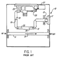
- Figure 1 shows a conventional system for producing a voltage responsive to RF power.
- Figure 2 shows the coupled port response within the coupler of Figure 1 with respect to frequency.
- Figure 3 shows the matching network response with respect to frequency of the matching network shown in Figure 1.
- Figure 4 shows the detector diode incident power response with respect to frequency for the detector shown in Figure 1.
- Figure 5 shows the preferred embodiment of an RF power detector according to the inventive principles.
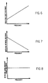
- Figure 6 shows the isolation port response for the coupler shown in Figure 5 with respect to frequency.
- Figure 7 shows the matching network response for the matching network shown in Figure 5 with respect to frequency.
- Figure 8 shows an improved and essentially flat response for the detector diode incident power response with respect to frequency for the detector shown in Figure 5.
- FIG. 1 a circuit schematic for a known (prior art) wideband power detector is shown in Figure 1.
- the power detector 10 is shown in Figure 1 by including a micro-strip directional coupler having a primary 11 and secondary 13.
- the isolation port for the secondary of the coupler is shown at 15 connected to a matching impedance 17.
- the coupled port 19 is shown connected at input 21 to a matching network shown as 23.
- a detector diode 25 is shown producing a detector voltage output at 27.
- the direction of propagation in the primary 11 of the coupler is shown by arrow 31.
- the primary direction of current propagation in the secondary 13 of the coupler is shown by arrow 33.
- a secondary direction of current propagation in the secondary 13 of the coupler is shown by arrow 35.
- An electromagnetically induced current in the secondary will produce a primary flow 33 in the opposite direction to the primary flow 31 in the coupler primary 11 and a secondary or counterflow 35 in the coupler secondary 13 which flows in the same direction as the of flow of current, in the primary 11, as shown by arrow 35.
- the coupled port 19 transfer characteristic or response with respect to a varying RF frequency is nonlinear as shown in Figure 2.
- This response may be nonlinear as shown or may be nonlinear, having several peaks, depending on the characteristic of the coupling network.
- the coupler isolation port 15 would have a matching or terminating resistor 17 and the coupling coefficient can be varied by the physical location or proximity of the secondary 13 with respect to the primary 11.
- the desired or preferred response of the detector 25 is flat with respect to RF frequency
- a matching network 23 response compensating the nonlinearity of the coupler may be as shown in Figure 3.
- attempting to produce a substantially flat detector response starting with the nonlinear coupled port 19 response at best attainable was a nonlinearly varying response as shown in Figure 4 by a ripple.
- a substantially flat detector diode incident power response to frequency is accomplished by reversing the secondary of the coupler and by using the secondary flow of current 35 in the coupler secondary 13 to produce a signal indicative of RF power out.
- RF current is made to flow within the primary of the coupler 11 as shown by arrow 31 from RF IN to RF OUT.
- a primary current shown by arrow 31 in primary 11 induces primary current 33 in the secondary 13 of the coupler.
- a secondary or counterflowing induced current in secondary 13 is shown by arrow 35 flowing opposite to that of the primary induced current 33. This secondary current 35 flows in the same direction as the current 31 in primary 11.
- the secondary current 35 should be zero or a minimal, under optimum design conditions, where the load impedance at the output of the coupler primary 11 matches the coupler output impedance. Under this impedance matching condition, a current reflected from the coupler primary 11 output port should be zero or minimal. Under the optimum impedance matching conditions, the induced current 35 flowing in the coupler secondary 13 toward the isolation port 15 should have no or minimal component due to any reflection in the coupler.
- the coupled port 19 is connected to terminating resistance 17.
- the termination or isolation port shown as 15 is coupled to the input 21 of the matching network 23.
- the direction of current flows in the secondary define the coupling and isolation ports.
- the counter or secondary induced current 35 flowing in the coupler secondary 13 is transmitted to the matching network 23 and through the matching network 23 to the detector diode 25, producing a detector voltage output 27.
- the induced current in coupler secondary 13 produces a substantially linear response at the isolation port 15 with respect to frequency, as shown in Figure 6. It is easier to compensate a linear varying response as shown in Figure 6, than the nonlinearly varying response as shown in Figure 2.
- the matching network 23 response may be designed to have a substantially linear transfer characteristic with respect to increasing frequency. In the preferred embodiment, where the response of the coupler with respect to increasing frequency is shown as substantially linear with a positive slope, the matching network 23 response over the same frequency range would be substantially linear and with a negative slope. Accordingly, the output of the coupler at the isolation port increases substantially linearly as the frequency of the RF current through the coupler primary is increased.
- the matching network response is made to decrease with respect to increasing frequency.
- the construction of the matching network 23 incorporates within it the junction capacitance of the detector diode.
- What is disclosed is a way of producing a substantially linear transfer responses with respect to frequency so an output signal is substantially flat with respect to a broadband frequency range.
Landscapes
- Engineering & Computer Science (AREA)
- Power Engineering (AREA)
- Physics & Mathematics (AREA)
- General Physics & Mathematics (AREA)
- Transmitters (AREA)
- Measurement Of Resistance Or Impedance (AREA)
- Microwave Amplifiers (AREA)
- Diaphragms For Electromechanical Transducers (AREA)
- Glass Compositions (AREA)
- Circuits Of Receivers In General (AREA)
Claims (13)
- Breitband-Leistungsdetektor (10), der mit einer Energiequelle verbunden ist und ein Ausgangssignal erzeugt, das die Leistung der Energiequelle über einem Frequenzband finiter Breite angibt und in bezug auf die Frequenz flach verläuft, mit folgenden Merkmalen: ein Richtungskuppler mit einem Primärschaltkreis (11) und einem Sekundärschaltkreis (13), wobei der Primärschaltkreis (11) mit einer Last verbunden ist, die eine Impedanz aufweist, welche an die Ausgangsimpedanz des Primärschaltkreises angepaßt ist, und wobei der Sekundärschaltkreis (13) einen Kopplungsanschluß (19), in dessen Richtung sich ein Primärstrom in dem Sekundärsekundärschaltkreis entgegengesetzt zu der Stromflußrichtung in dem Primärschaltkreis ausbreitet, und einen Isolationsanschluß (15) aufweist, in dessen Richtung sich ein Sekundärstrom in dem Sekundärschaltkreis gleichgerichtet zu der Stromflußrichtung in dem Primärschaltkreis ausbreitet; und ein Anpassungsnetzwerk (23) mit einem Eingangsanschluß (21) und einem Ausgangsanschluß, wobei der Eingangsanschluß des Anpassungsnetzwerkes mit dem Isolationsanschluß (15) verbunden ist, dadurch gekennzeichnet, daß der Koppler (11, 13) die Energiequelle mit dem Isolationsanschluß (15) koppelt, um ein Ausgangssignal an dem Isolationsanschluß (15) zu erzeugen, das sich über dem endlichen Frequenzband im wesentlichen linear mit der Frequenz ändert, das Anpassungsnetz (23) eine Übertragungsfunktion vom Eingangs- zum Ausgangsanschluß hat, welche diese im wesentlichen lineare Änderung des Ausgangssignal am Isolationsanschluß (15) in bezug auf die Frequenz kompensiert, und das Anpassungsnetzwerk (23) über dem endlichen Frequenzband ein flaches Ausgangssignal in bezug auf die Frequenz erzeugt.
- Leistungsdetektor (10) nach Anspruch 1, bei dem die Übertragungsfunktion vom Eingang zum Ausgang des Übertragungsnetzwerks (23) über dem Frequenzband endlicher Breite zu dem sich linearen ändernden Ausgangssignal an dem Isolationsanschluß (15) entgegengesetzt oder invers ist.
- Leistungsdetektor (10) nach Anspruch 1 oder 2, bei dem der Koppler eine angepaßte Impedanz (17) aufweist, die mit dem Kopplungsanschluß (19) verbunden ist.
- Leistungsdetektor (10) nach einem der Ansprüche 1 bis 3, bei dem eine Detektorvorrichtung (25) mit dem Ausgangsanschluß des Anpassungsnetzwerkes (23) verbunden ist und ein Signal erzeugt, das die Leistung von der Energiequelle abhängig von dem Ausgangssignal des Anpassungsnetzwerkes (23) an dem Ausgangsanschluß angibt.
- Leistungsdetektor (10) nach Anspruch 4, bei dem die Detektorvorrichtung ein Diodendetektor (35) mit einer internen Übergangskapazität ist und das Anpassungsnetzwerk (23) diese Übergangskapazität umfaßt.
- Leistungsdetektor (10) nach einem der vorangehenden Ansprüche, bei dem der Sekundärstrom in dem Sekundärschaltkreis (13) des Kopplers (11, 13) sich im wesentlichen in der Richtung des Stroms in dem Primärschaltkreis (11) des Kopplers (11, 13) als eine reflektierte Welle ausbreitet.
- Leistungsdetektor (10) nach Anspruch 6, bei dem das Ausgangssignal bei dem Isolationsanschluß (15) mit zunehmender Frequenz zunimmt und die Übergangsfunktion vom Eingang zum Ausgang des Anpassungsnetzwerkes (23) mit zunehmender Frequenz abnimmt.
- Leistungsdetektor (10) nach Anspruch 7, bei dem die Übertragungsfunktion des Anpassungsnetzwerkes (23) mit einer Rate abnimmt, die im wesentlichen gleich der Rate der Zunahme des Ausgangssignals am Isolationsanschluß (15) bei zunehmender Frequenz ist.
- Verfahren zum Erzeugen eines Leistungsanzeigesignals, das über einem Frequenzband finiter Breite in bezug auf die Frequenz flach verläuft, mit folgenden Verfahrensschritten: Verbinden eines Primärschaltkreises (11) eines Richtungskopplers (11, 12) mit einer Energiequelle, die Frequenzen hat, welche sich über einem Frequenzband finiter Breite ändern; Verbinden eines Ausgangsanschlußes des Primärschaltkreises mit einer angepaßten Impedanz; Verbinden einer angepaßten Impedanz (17) mit einem Kopplungsanschluß (19) eines Sekundärschaltkreises (13) des Kopplers (11, 13), wobei in Richtung auf diesen Kopplungsanschluß (19) ein Strom in dem Sekundärschaltkreis (13) in entgegengesetzter Richtung zum Stromfluß in dem Primärschaltkreis (11) fließt; und Verbinden eines Anpassungsnetzwerkes (23) mit einem Isolationsanschluß (15) des Sekundärschaltkreises (13) des Kopplers (11, 13), wobei in Richtung dieses Isolationsanschlusses (15) Strom in dem Sekundärschaltkreis (13) gleichgerichtet zur Stromflußrichtung in dem Primärschaltkreis (11) fließt; dadurch gekennzeichnet, daß der Isolationsanschluß (15) mit der Energiequelle gekoppelt wird, um an dem Isolationsanschluß (15) ein Signal zu erzeugen, das sich über dem finiten Frequenzband im wesentlichen linear mit der Frequenz ändert, das Signal an dem Isolationsanschluß (15) zu dem Anpassungsnetzwerk (23) übertragen wird, das eine lineare Übertragungsfunktion in bezug auf die Frequenz hat und das sich linear ändernde Signal an dem Isolationsanschluß (15) ausgleicht, und über dem Frequenzband finiter Breite an dem Ausgang des Anpassungsnetzwerkes (23) ein flaches Ausgangssignal in bezug auf die Frequenz erzeugt wird.
- Verfahren nach Anspruch 9 mit dem weiteren Verfahrensschritt: Verwenden eines Anpassungsnetzwerkes (23) mit einer linear abnehmenden Übertragungsfunktion bei einer zunehmenden Frequenz, wobei das Ausgangssignal an dem Isolationsanschluß (15) mit zunehmender Frequenz linear zunimmt.
- Verfahren nach Anspruch 10 mit weiterem Verfahrensschritt: Verbinden eines Diodendetektors (25) mit dem Ausgangssignal am Ausgang des Anpassungsnetzwerkes (23), um das Leistungsanzeigesignal zu erzeugen.
- Verfahren nach Anspruch 11, bei dem die Übergangskapazität des Diodendetektors (35) zu einem Teil des Anpassungsnetzwerkes (23) gemacht wird.
- Verfahren nach Anspruch 12, bei dem ein Stromfluß in dem Sekundärschaltkreis (13) des Kopplers (11, 13) induziert wird und der in dem Sekundärschaltkreis (13) des Kopplers induzierte Strom an das Anpassungsnetzwerk (23) übertragen wird.
Applications Claiming Priority (2)
| Application Number | Priority Date | Filing Date | Title |
|---|---|---|---|
| US07/992,310 US5325064A (en) | 1992-12-21 | 1992-12-21 | Wideband flat power detector |
| US992310 | 2001-11-19 |
Publications (3)
| Publication Number | Publication Date |
|---|---|
| EP0604203A2 EP0604203A2 (de) | 1994-06-29 |
| EP0604203A3 EP0604203A3 (de) | 1995-05-17 |
| EP0604203B1 true EP0604203B1 (de) | 1999-04-14 |
Family
ID=25538171
Family Applications (1)
| Application Number | Title | Priority Date | Filing Date |
|---|---|---|---|
| EP93310401A Expired - Lifetime EP0604203B1 (de) | 1992-12-21 | 1993-12-21 | Breitbandig flacher Leistungsdetektor |
Country Status (8)
| Country | Link |
|---|---|
| US (1) | US5325064A (de) |
| EP (1) | EP0604203B1 (de) |
| JP (1) | JPH06273460A (de) |
| CN (1) | CN1052305C (de) |
| CA (1) | CA2112089C (de) |
| DE (1) | DE69324459T2 (de) |
| MY (1) | MY109853A (de) |
| NO (1) | NO310086B1 (de) |
Families Citing this family (13)
| Publication number | Priority date | Publication date | Assignee | Title |
|---|---|---|---|---|
| US5473287A (en) * | 1994-11-14 | 1995-12-05 | Micronetics, Inc. | Electronic oscillator with transmission line tuning of phase noise and linearity |
| SE503922C2 (sv) * | 1994-11-17 | 1996-09-30 | Lg Products Ab | Mätledning för en koaxialleding för bestämning av genomgående energiflöde och ståendevågförhållande |
| FR2745091B1 (fr) * | 1996-02-15 | 1998-04-24 | Matra Communication | Dispositif de mesure de puissance radiofrequence |
| JP3744249B2 (ja) | 1999-03-29 | 2006-02-08 | 株式会社村田製作所 | 送信出力制御装置及びそれを用いた無線機器 |
| US6600307B2 (en) * | 2000-03-02 | 2003-07-29 | Sarnoff Corporation | Method and apparatus for measuring true transmitted power using a broadband dual directional coupler |
| JP2002152059A (ja) * | 2000-11-14 | 2002-05-24 | Sharp Corp | 送信電力制御回路 |
| DE10205359A1 (de) * | 2002-02-08 | 2003-08-21 | Rohde & Schwarz | Leistungsdetektor mit Gleichspannungsentkopplung |
| US7202760B2 (en) * | 2004-06-01 | 2007-04-10 | Werlatone, Inc. | Resistive voltage divider |
| CN101635943B (zh) * | 2008-07-24 | 2012-01-11 | 中兴通讯股份有限公司 | 宽带功率检测方法和装置 |
| JP2010088011A (ja) * | 2008-10-02 | 2010-04-15 | Panasonic Corp | 方向性結合器 |
| US9077064B2 (en) | 2009-11-24 | 2015-07-07 | Telefonaktiebolaget L M Ericsson (Publ) | Microwave transmission assembly |
| CN102226821A (zh) * | 2011-03-24 | 2011-10-26 | 电子科技大学 | 一种用于波导信号功率检测的传输式检波器 |
| CN104183896B (zh) * | 2014-08-11 | 2016-11-09 | 电子科技大学 | 适用于太赫兹频段的四端口器件测试结构 |
Family Cites Families (10)
| Publication number | Priority date | Publication date | Assignee | Title |
|---|---|---|---|---|
| US2562281A (en) * | 1944-06-14 | 1951-07-31 | Bell Telephone Labor Inc | Directive pickup for transmission lines |
| JPS53147450A (en) * | 1977-05-27 | 1978-12-22 | Mitsubishi Electric Corp | Directional coupler |
| JPS5523652A (en) * | 1978-08-07 | 1980-02-20 | Fujitsu Ltd | Detector |
| JPS5698659A (en) * | 1980-01-10 | 1981-08-08 | Nec Corp | Microwave power monitoring circuit |
| GB8413339D0 (en) * | 1984-05-24 | 1984-06-27 | Secr Defence | Six-port reflectometer |
| US5111165A (en) * | 1989-07-11 | 1992-05-05 | Wiltron Company | Microwave coupler and method of operating same utilizing forward coupling |
| US5012209A (en) * | 1990-01-12 | 1991-04-30 | Raytheon Company | Broadband stripline coupler |
| FR2667999B1 (fr) * | 1990-10-10 | 1996-11-22 | Alcatel Espace | Dispositif micro-onde correcteur de pente, notamment dans le domaine spatial. |
| US5159298A (en) | 1991-01-29 | 1992-10-27 | Motorola, Inc. | Microstrip directional coupler with single element compensation |
| US5204614A (en) * | 1991-08-14 | 1993-04-20 | Hewlett-Packard Company | Broad-band microwave power sensor using diodes above their resonant frequency |
-
1992
- 1992-12-21 US US07/992,310 patent/US5325064A/en not_active Expired - Fee Related
-
1993
- 1993-12-21 NO NO934733A patent/NO310086B1/no not_active IP Right Cessation
- 1993-12-21 MY MYPI93002780A patent/MY109853A/en unknown
- 1993-12-21 DE DE69324459T patent/DE69324459T2/de not_active Expired - Fee Related
- 1993-12-21 CN CN93112792.0A patent/CN1052305C/zh not_active Expired - Fee Related
- 1993-12-21 CA CA002112089A patent/CA2112089C/en not_active Expired - Fee Related
- 1993-12-21 EP EP93310401A patent/EP0604203B1/de not_active Expired - Lifetime
- 1993-12-21 JP JP5345442A patent/JPH06273460A/ja active Pending
Also Published As
| Publication number | Publication date |
|---|---|
| CN1089358A (zh) | 1994-07-13 |
| JPH06273460A (ja) | 1994-09-30 |
| US5325064A (en) | 1994-06-28 |
| DE69324459T2 (de) | 1999-11-18 |
| EP0604203A3 (de) | 1995-05-17 |
| DE69324459D1 (de) | 1999-05-20 |
| CN1052305C (zh) | 2000-05-10 |
| NO934733D0 (no) | 1993-12-21 |
| CA2112089C (en) | 2001-05-29 |
| CA2112089A1 (en) | 1994-06-22 |
| NO934733L (no) | 1994-06-22 |
| EP0604203A2 (de) | 1994-06-29 |
| MY109853A (en) | 1997-09-30 |
| NO310086B1 (no) | 2001-05-14 |
Similar Documents
| Publication | Publication Date | Title |
|---|---|---|
| US5325064A (en) | Wideband flat power detector | |
| US3701057A (en) | Broad-band lumped-element directional coupler | |
| EP1355162B1 (de) | Kapazitiv arbeitender HF-Leistungssensor zur Messung eines HF-Leistungssignals | |
| CN115425964B (zh) | 基于pt对称原理的频率可调非互易传输系统及其检测方法 | |
| US4467293A (en) | Ferrite type directional coupler | |
| US5204614A (en) | Broad-band microwave power sensor using diodes above their resonant frequency | |
| WO1982004317A1 (en) | Impedance measurement circuit | |
| US6690177B2 (en) | Frequency selective improvement of the directivity of a return loss bridge | |
| US4415852A (en) | Single hybrid junction frequency discriminator | |
| US5245278A (en) | Device for the processing of a signal coming from a sensor with a derivative type of response | |
| US5420464A (en) | RF voltage/current sensor apparatus | |
| JPH07202501A (ja) | 高周波検波回路 | |
| US20060197627A1 (en) | Low-loss directional bridge | |
| JPH06235744A (ja) | マイクロ波電力検出器 | |
| De Jong | Measuring the propagation time of coaxial cables used with GPS receivers | |
| SU1327019A1 (ru) | Устройство дл измерени комплексного коэффициента передачи СВЧ четырехполюсников | |
| SU1278735A1 (ru) | Автоматический измеритель параметров СВЧ-четырехполюсников | |
| GB2266155A (en) | Measuring standing wave ratios | |
| KR0114470Y1 (ko) | 통신기기용 매칭 트랜스 동작 감쇠량 및 삽입손실량 측정회로 | |
| JPH07105653B2 (ja) | 方向性結合器 | |
| JPH07254833A (ja) | クロック信号位相安定化回路 | |
| Lin et al. | Four kinds of microwave measurements to make use of an automatic slotted-line system | |
| JPS56157876A (en) | Measurement of load characteristics of high frequency field effect transistor | |
| JPH06105841B2 (ja) | 方向性結合器 | |
| JPS5932922B2 (ja) | 方向性結合器 |
Legal Events
| Date | Code | Title | Description |
|---|---|---|---|
| PUAI | Public reference made under article 153(3) epc to a published international application that has entered the european phase |
Free format text: ORIGINAL CODE: 0009012 |
|
| AK | Designated contracting states |
Kind code of ref document: A2 Designated state(s): DE FR GB IT SE |
|
| RIN1 | Information on inventor provided before grant (corrected) |
Inventor name: WU, WANG CHIU Inventor name: LEANES, JAMES A. |
|
| PUAL | Search report despatched |
Free format text: ORIGINAL CODE: 0009013 |
|
| AK | Designated contracting states |
Kind code of ref document: A3 Designated state(s): DE FR GB IT SE |
|
| 17P | Request for examination filed |
Effective date: 19951103 |
|
| 17Q | First examination report despatched |
Effective date: 19971208 |
|
| GRAG | Despatch of communication of intention to grant |
Free format text: ORIGINAL CODE: EPIDOS AGRA |
|
| GRAG | Despatch of communication of intention to grant |
Free format text: ORIGINAL CODE: EPIDOS AGRA |
|
| GRAH | Despatch of communication of intention to grant a patent |
Free format text: ORIGINAL CODE: EPIDOS IGRA |
|
| GRAH | Despatch of communication of intention to grant a patent |
Free format text: ORIGINAL CODE: EPIDOS IGRA |
|
| GRAA | (expected) grant |
Free format text: ORIGINAL CODE: 0009210 |
|
| AK | Designated contracting states |
Kind code of ref document: B1 Designated state(s): DE FR GB IT SE |
|
| REF | Corresponds to: |
Ref document number: 69324459 Country of ref document: DE Date of ref document: 19990520 |
|
| ET | Fr: translation filed | ||
| PLBE | No opposition filed within time limit |
Free format text: ORIGINAL CODE: 0009261 |
|
| STAA | Information on the status of an ep patent application or granted ep patent |
Free format text: STATUS: NO OPPOSITION FILED WITHIN TIME LIMIT |
|
| 26N | No opposition filed | ||
| REG | Reference to a national code |
Ref country code: GB Ref legal event code: IF02 |
|
| PGFP | Annual fee paid to national office [announced via postgrant information from national office to epo] |
Ref country code: GB Payment date: 20031217 Year of fee payment: 11 |
|
| PGFP | Annual fee paid to national office [announced via postgrant information from national office to epo] |
Ref country code: FR Payment date: 20031218 Year of fee payment: 11 |
|
| PGFP | Annual fee paid to national office [announced via postgrant information from national office to epo] |
Ref country code: SE Payment date: 20031219 Year of fee payment: 11 |
|
| PGFP | Annual fee paid to national office [announced via postgrant information from national office to epo] |
Ref country code: DE Payment date: 20040202 Year of fee payment: 11 |
|
| PG25 | Lapsed in a contracting state [announced via postgrant information from national office to epo] |
Ref country code: GB Free format text: LAPSE BECAUSE OF NON-PAYMENT OF DUE FEES Effective date: 20041221 |
|
| PG25 | Lapsed in a contracting state [announced via postgrant information from national office to epo] |
Ref country code: SE Free format text: LAPSE BECAUSE OF NON-PAYMENT OF DUE FEES Effective date: 20041222 |
|
| PG25 | Lapsed in a contracting state [announced via postgrant information from national office to epo] |
Ref country code: DE Free format text: LAPSE BECAUSE OF NON-PAYMENT OF DUE FEES Effective date: 20050701 |
|
| EUG | Se: european patent has lapsed | ||
| GBPC | Gb: european patent ceased through non-payment of renewal fee |
Effective date: 20041221 |
|
| PG25 | Lapsed in a contracting state [announced via postgrant information from national office to epo] |
Ref country code: FR Free format text: LAPSE BECAUSE OF NON-PAYMENT OF DUE FEES Effective date: 20050831 |
|
| REG | Reference to a national code |
Ref country code: FR Ref legal event code: ST |
|
| PG25 | Lapsed in a contracting state [announced via postgrant information from national office to epo] |
Ref country code: IT Free format text: LAPSE BECAUSE OF NON-PAYMENT OF DUE FEES;WARNING: LAPSES OF ITALIAN PATENTS WITH EFFECTIVE DATE BEFORE 2007 MAY HAVE OCCURRED AT ANY TIME BEFORE 2007. THE CORRECT EFFECTIVE DATE MAY BE DIFFERENT FROM THE ONE RECORDED. Effective date: 20051221 |