EP0602906B1 - Synchronous processing method and apparatus for a plurality of processors executing a plurality of programs in parallel - Google Patents
Synchronous processing method and apparatus for a plurality of processors executing a plurality of programs in parallel Download PDFInfo
- Publication number
- EP0602906B1 EP0602906B1 EP93309957A EP93309957A EP0602906B1 EP 0602906 B1 EP0602906 B1 EP 0602906B1 EP 93309957 A EP93309957 A EP 93309957A EP 93309957 A EP93309957 A EP 93309957A EP 0602906 B1 EP0602906 B1 EP 0602906B1
- Authority
- EP
- European Patent Office
- Prior art keywords
- synchronous
- processing
- group
- status information
- processing elements
- Prior art date
- Legal status (The legal status is an assumption and is not a legal conclusion. Google has not performed a legal analysis and makes no representation as to the accuracy of the status listed.)
- Expired - Lifetime
Links
Images


Classifications
-
- G—PHYSICS
- G06—COMPUTING; CALCULATING OR COUNTING
- G06F—ELECTRIC DIGITAL DATA PROCESSING
- G06F8/00—Arrangements for software engineering
- G06F8/40—Transformation of program code
- G06F8/41—Compilation
- G06F8/45—Exploiting coarse grain parallelism in compilation, i.e. parallelism between groups of instructions
- G06F8/458—Synchronisation, e.g. post-wait, barriers, locks
Definitions
- the present invention relates to a synchronous processing method and apparatus for a plurality of processors, and more particularly, to a method and apparatus in which a plurality of processors execute a plurality of programs in parallel and in synchronism.
- the individual processors for effecting the parallel processing have to execute processes containing a plurality of phases in some cases.
- This synchronous processing is conducted by the following actions. To start with, the processor which has finished its processing the earliest detects that a synchronous waiting status is reached, and waits for an end of the processing by another processor before synchronization begins, i.e. this processor waits until all other processors reach the synchronous waiting status, so that the processors may become synchronized. Then, upon detecting that all the processors have reached the synchronous waiting status, all the processors execute the synchronization process discussed below.
- Synchronous processing is conducted by a synchronous processing element provided in each processor.
- This synchronous processing element includes a synchronous status register, a synchronous receiving element and a synchronous detecting element.
- the processor which has finished its processing earliest sets, in its synchronous status register, a piece of synchronous status information (e.g., "1") indicating that the processor has reached the synchronous waiting status.
- this synchronous status information is transmitted via a communication unit to all other processors.
- the synchronous status information is set in the synchronous receiving elements in all other processors.
- the processors which have finished their processings set the synchronous status information in their own synchronous status register. This synchronous status information is transmitted to all other processors.
- the transmitted synchronous status information is set in the synchronous receiving elements in all of the other processors.
- the processor which has terminated its processing last sets the synchronous status information in its status register.
- This synchronous status information is then transmitted to the synchronous receiving elements in all other processors.
- the synchronous detecting element in each processor detects all of the synchronous status information, corresponding to the number of processors, which have been received in the synchronous receiving element. Then, the processors shift to the next processing on the assumption that all the processors are now synchronized.
- the above-mentioned synchronous processing element includes a synchronous status register, a synchronous receiving element and a synchronous detecting element, each capable only of storing the data "1". Therefore, only one process (one program) can be executed by one processor. Further, the synchronous processing element is incapable of assigning a certain program to one group of processors to be synchronized among the group of processors and assigning another program to a second group of processors to be synchronized among the second group. For this reason, it is impossible to execute, with high efficiency, a plurality of parallel processing programs.
- Another synchronous processing apparatus may be considered to comprise:
- Synchronous processing apparatus embodying a first aspect of the present invention is characterised in that each said processing element of the said plurality includes synchronous processing means having:
- the program process may be executed while each processing element becomes synchronized by transferring the status information between the plurality of processing elements.
- the processing elements are, e.g., processors and the communication means are, e.g., a communication network.
- a storage control element may cause the synchronous status storage element repeatedly and alternately to store synchronous status information "1" and synchronous status information "0" per processing.
- the storage control element may also cause the synchronization combination storage element to store the synchronization combination information.
- the storage control element and the processing shift element may be provided in an instruction processing element for executing a plurality of instructions.
- the synchronous receiving element for receiving the synchronous status information transmitted from all the processing elements and for outputting the received synchronous status information to the synchronous judging element may be a register, the bit number of which corresponds to the number of the plurality of processing elements. This register stores, when receiving the synchronous status information, the synchronous status information in bit strings corresponding to the plurality of processing elements.
- the synchronous judging element may include a logic operation circuit for performing a logic operation between the synchronous status information given from the synchronous receiving element and the synchronization combination information given from the synchronization combination storage element, thereby determining whether the processing elements indicated by the synchronization combination information are synchronized.
- the synchronization combination storage element may be a register the bit number of which corresponds to the number of the plurality of processing elements. This register may store synchronous status information "1" in a bit string corresponding to all the processing elements indicated by the synchronization combination information among the bit strings corresponding to the plurality of processing elements.
- the processing shifting element may be provided with a synchronous indicating register for storing synchronous indicating information for indicating whether the processing elements indicated by the synchronization combination information are synchronized.
- the processing element may be a control register for allocating this register to each processing element.
- the control register may be a 1-bit register which allocates the processing elements to take two kinds of synchronization information in accordance with pieces of control information "1" and "0" for executing the processing of two programs.
- the synchronous receiving element may be provided with a parity error detecting element for detecting a parity error of the information on the broadcasting line through which the information is broadcasted to the respective processing elements.
- the processing elements when the parity error detecting element detects the 1-bit error, may continue the processing without interrupting the processing of the programs. However, when further detecting a 1-bit error after detecting the former 1-bit error, the processing may be interrupted in the processing element.
- synchronous processing apparatus comprising: a plurality of processing elements for executing processes of a plurality of programs, a group of the processing elements being assignable to a corresponding one of the programs so that processes of that program can be executed in parallel and in synchronism by the processing elements of the said group, each processing element belonging to such a group being operable, when it completes one of the said processes of the program corresponding to that group, to transmit synchronous status information indicating that it has reached a synchronization waiting status; communication means through which information is transferred between the processing elements of the said plurality; synchronous judging means for judging whether such a group of processing elements are in synchronism; and shifting means operable, when said synchronous judging means judges that such a group of processing elements are in synchronism, to cause that group of processing elements to execute a next process in the program corresponding to that group; characterised in that each said processing element of the said plurality includes synchronous processing means having: a plurality of synchronous status
- the plurality of synchronous status storage elements are provided corresponding to a plurality of programs.
- the synchronous status storage elements respectively store synchronous status information showing that a synchronization waiting status is reached when a self-processing element finishes the processing.
- a storage control element may cause each of the plurality of synchronous status storage elements to store the synchronous status information and transmits the synchronous status information to all the processing elements.
- a plurality of synchronous judging elements are provided corresponding to the plurality of synchronous status storage elements. The synchronous judging elements respectively judge whether the other processing elements are synchronized.
- a processing shifting element when any one of the plurality of synchronous judging elements judges that the processing elements are synchronized, shifts all the processing elements to the next processing of the program corresponding to that synchronous judging element.
- a selecting element for selecting any one of synchronous processing of a plurality of programs and synchronous processing of one program, which is to be performed by the plurality of synchronous status storage elements and by the plurality of synchronous judging elements.
- the selecting element may be a register controlled by the storage control element.
- the synchronous judging element may include a plurality of synchronous receiving elements for receiving the synchronous status information transmitted from all the processing elements and storing the received synchronous status information.
- a plurality of synchronous broadcasting lines may be further provided through which the synchronous status information is transmitted corresponding to the plurality of synchronous receiving elements and a mode circuit for connecting each broadcasting line to the synchronous receiving element corresponding to the broadcasting line when processing a plurality of programs and connecting each broadcasting line to one synchronous receiving element when processing one program.
- the stored synchronization combination information indicates the combination of the processing elements to take the synchronization per program in order to process some programs by the plurality of processing elements.
- Stored subsequently may be the synchronous status information showing that the synchronous waiting status is reached when the self processing element has finished the processing.
- the synchronous status information is transmitted to all other processing elements.
- the next step is to judge whether the processing elements indicated by the synchronization combination information are synchronized.
- all the processing elements indicated by the synchronization combination information are shifted to the next processing of the program corresponding to the synchronization combination information. That is, it is possible to designate the combination of the processing elements to take the synchronization per program on the basis of the synchronization combination information.
- a synchronous processing method for use in synchronous processing apparatus having a plurality of processing elements, a group of which processing elements can be assigned to execute a corresponding program so that processes of the program can be executed in parallel and in synchronism by the processing elements of the group which method comprises the steps of: storing, at each processing element of the said plurality, synchronization combination information indicating the processing elements of the said plurality that belong to such a group; when a processing element belonging to such a group completes one of the said processes of its corresponding program, storing, in the processing element concerned, synchronous status information indicating that the processing element concerned has reached a synchronization waiting status; transmitting the stored synchronous status information from each processing element of the said plurality to all of the other processing elements of the said plurality; at each processing element, receiving the transmitted synchronous status information from the other processing elements of the said plurality; at each processing element, judging whether the processing elements of the group to which the processing element concerned belongs are in synchronism
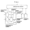
- FIGURE 1 illustrates a concept of a synchronous processing apparatus embodying the present invention.
- Processing elements 1 communicate with each other through communication network 2.
- Each processing element 1 includes a synchronous status storage element 12, a synchronization combination storage element 11, a synchronous judging element 13a, a processing shifting element 8b and a storage control element 8a.
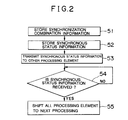
- FIGURE 2 is a flowchart illustrating a concept of a synchronous processing method according to the present invention.
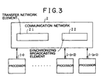
- FIGURE 3 is a block diagram showing an architecture of the synchronous processing apparatus in a first embodiment of this invention.
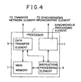
- FIGURE 4 is a block diagram illustrating a configuration of a processor in the first embodiment.
- the synchronous processing apparatus is provided with a plurality of processors for executing program instructions.
- the synchronous processing apparatus is also provided with a communication network 2 for connecting the plurality of processors 1-0 ⁇ 1-(n-1) to each other and transmitting receiving data and information between the processors 1.
- the communication network 2 includes a transfer network element 21 and a synchronizing broadcasting element 22.
- the transfer network element 21 effects a transfer of data to a data transfer element 9, shown in FIGURE 4, provided in each of the processors 1-0 ⁇ 1-(n-1).
- the synchronizing broadcasting element 22 broadcasts a synchronous status of each of the processors 1-0 ⁇ 1-n to a synchronous processing element 10, shown in FIGURE 4.
- Each of the processors 1-0 ⁇ 1-n(n-1), as shown in FIGURE 4 includes a main memory 7, an instruction processing element 8, a data transfer element 9 and a synchronous processing element 10.
- the main memory 7 stores a program including a plurality of instructions and also stores data.
- the instruction processing element 8 connected to the main memory 7 fetches an instruction out of the program of the main memory 7 and executes this instruction.
- the data transfer element 9 is connected to the main memory 7, the instruction processing element 8 and the transfer network element 21.
- the data transfer element 9 transfers the data between the main memory 7 and the transfer network element 21.
- Instruction processing element 8 corresponds to storage control element 8a and processing shifting element 8b of FIGURE 1.
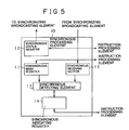
- FIGURE 5 is a block diagram showing a construction of the synchronous processing element 10.
- the synchronous processing element 10 is connected to the instruction processing element 8 and the synchronizing broadcasting element 22.
- the synchronous processing element 10 performs synchronous processing for each processor.
- Synchronous processing element 10 includes a synchronous status register 12, a synchronous mask register 11, a synchronous receiving element 15, a synchronous detecting element 13 and a synchronous indicating register 14.
- the synchronous status register 12 is accessed by the instruction processing element 8.
- the synchronous status register 12 is defined as a 1-bit length register for storing synchronous status information indicating that a synchronization waiting status for synchronization with another processor is reached, when the processor completes an execution of a program process.
- the synchronous status register 12 stores, e.g., a piece of synchronous status information "1", in accordance with the program when reaching the status to be synchronized with another processor by ending a program process.
- the synchronous mask register 11, corresponding to synchronization combination storage element 11 of FIGURE 1, is accessed by the instruction processing element 8 and is an n-bit length register for storing synchronization combination information.
- n represents the number of processors.
- This synchronous mask register 11 stores, e.g., the synchronization combination information "1", with respect to other processors that are to be synchronized with its processor.
- the synchronous mask register 11, however, also stores synchronization combination information "0" with respect to other processors that are not to be synchronized with its processor.
- the synchronous receiving element 15 is connected to the synchronizing broadcasting element 22.
- the synchronous receiving element 15 is a register for receiving the synchronous status information of the other processors' synchronous status registers 12 which is broadcast from the synchronizing broadcasting element 22 and for retaining this synchronous status information.
- the synchronous detecting element 13 is connected to the synchronous mask register 11 and the synchronous receiving element 15.
- Synchronous judging element 13a of FIGURE 1 corresponds to synchronous detecting element 13, synchronous receiving element 15, and synchronous indicating register 14 of Figure 5.
- Synchronous detecting element 13 is a combination circuit for detecting a status where the synchronous status information is all "1" and a status where the synchronous status information is all "0".
- the synchronous indicating register 14 is a 1-bit length register for indicating synchronous statuses of all the processors conceived as targets.
- the synchronous indicating register 14 is accessed by the instruction processing element 8 and set or reset by the synchronous detecting element 13.
- the synchronous detecting element 13 transmits a set signal to the synchronous indicating register 14.
- the set signal is transmitted when the synchronous status information of all of the processors to be synchronized is "1".
- These processors, for which the synchronous status information must all be “1"s, are the processors for which the synchronization combination information of the synchronous mask register 11 is "1".
- Synchronous detecting element 13 sets “1” in synchronous indicating register 14 by a logic operation of the synchronization combination information "1” and the synchronous status information "1" from all of the processors to be synchronized.
- Instruction processing element 8 shifts to a next process when "1" is set in synchronous indicating register 14. Instruction processing element 8 then resets synchronous status register 12 to "0".
- the synchronous detecting element 13 transmits a reset signal to the synchronous indicating register 14 in the next process.
- the reset signal is transmitted when the synchronous status information is all "0" for the processors to be synchronized, i.e. the processors for which the synchronization combination information of the synchronous mask register 11 is "1".
- Synchronous detecting element 13 resets synchronous indicating register 14 to "0” by the logic operation of the synchronization combination information "1" and the synchronous status information "0" from all of the processors to be synchronized in the next process.
- Instruction processing element 8 shifts to a next process by resetting synchronous indicating register 14 to "0".
- Instruction processing element 8 sets synchronous status register 12 to "1".
- synchronous status register 12 alternately repeats the above-described set or reset action.
- Synchronous indicating register 14 also alternately repeats the above-described set or reset action.
- FIGURE 6 is a diagram illustrating an example of a configuration of the synchronous mask register 11. As illustrated in FIGURE 6, a bit string i corresponds to a processor i.
- FIGURE 7 is a diagram showing contents of the synchronous mask register 11 when running the two programs A and B.
- FIGURE 8 is a flowchart showing the processing of the program A. As illustrated in FIGURE 7, it is assumed that e.g., eight processors 1-0 ⁇ 1-7 are available. It is also presumed, in this example, that the program A is executed by the processors 1-0, 1-1, 1-3, 1-4, 1-5, while the program B is executed by the processors 1-2, 1-6, 1-7.
- an 8-bit pattern "11011100", indicating processors 1-0, 1-1, 1-3, 1-4, and 1-5, is set as a piece of synchronization combination information in the synchronous mask register 11 included in each of the processors 1-0, 1-0, 1-3, 1-4, 1-5 (step 101).
- the processors 1-0, 1-1, 1-3, 1-4, 1-5 execute the program A while being synchronized, the synchronous status information of the synchronous status register 12 of each processor and the information of the synchronous indicating register 14 thereof are set to "0".
- the processors 1-0, 1-1, 1-3, 1-4, 1-5 start executing processing k (step 102).
- k is initially 1, however, its value is incremented when repeating the process.
- the processors are at a status to take processor-to-processor synchronization on the program A.
- the instruction processing element 8 sets the synchronous status information of the synchronous status register 12 to "1" (step 103).
- the synchronous status information "1" of the synchronous status register 12 is transmitted to the synchronizing broadcasting element 22 in the communication network 2 under control of the instruction processing element 8 (step 104).
- the synchronous status information "1" is broadcast to all other processors from the synchronizing broadcasting element 22.
- the synchronous receiving elements 15 of the respective processors receive pieces of synchronous status information "1" of the synchronous status registers 12 of all the processors.
- the synchronous detecting element 13 performs a logic operation with respect to the synchronous status information of the synchronous receiving element 15 and the synchronization combination information of the synchronous mask register 11, thereby detecting synchronization (step 105). If synchronization is not detected, there is a waiting period for receiving the next synchronous status information (step 106).
- the instruction processing element 8 of each processor executing the program A has already set "1" in the synchronous status register 12.
- the instruction processing element 8 monitors the synchronous indicating register 14 and judges whether or not 1 is set in the information of the synchronous indicating register 14 (step 107). Herein, if 1 is not set in the information of the synchronous indicating register 14, there is a waiting period until the information becomes 1 (step 106). Next, when receiving the synchronous information from all the processors indicated by the synchronization combination information, the information of the synchronous indicating register 14 becomes "1". The action thereof will be explained below.
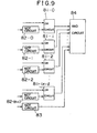
- FIGURE 9 is a block diagram showing a configuration of the synchronous detecting element 13 for setting "1" in the synchronous indicating register 14.
- OR circuits 81-0 ⁇ 81-(n-1) are provided in FIGURE 9 for setting "1" in the synchronous indicating register 14.
- NOT circuits 82-0 ⁇ 82-(n-1) are provided in FIGURE 9 for setting "1" in the synchronous indicating register 14.
- AND circuit 84 is provided in FIGURE 9 .
- the synchronous status information of the processors 1-0 ⁇ 1-(n-1) which has been inputted from the synchronous receiving element 15 is inputted to the corresponding OR circuits 81-0 ⁇ 81-(n-1).
- the synchronous status information of the processor 1-1 is inputted to the OR circuit 81-1 from the synchronous receiving element 15.
- Synchronization combination information "11011100” from bit 0 to bit n-1 which has been outputted from the synchronous mask register 11 is inputted to the corresponding NOT circuits 82-0 ⁇ 82-(n-1). Further, information "0" from the synchronous indicating register 14 is inputted to the NOT circuit 83.
- the instruction processing element 8 when reaching a processor-to-processor synchronization status, sets "0" in the synchronous status register 12 (step 109).
- the synchronous status information "0" of the synchronous status register 12 is transmitted to the synchronizing broadcasting element 22 on the network 2 (step 110).
- the synchronous status information "0" is broadcast to all other processors from the synchronizing broadcasting element 22.
- the synchronous receiving elements 15 of the respective processors receive pieces of synchronous status information "0" of the synchronous status registers 12 of all other processors.
- the synchronous detecting element 13 executes the logic operation with respect to the synchronous status information of the synchronous receiving element 15 and the synchronization combination information of the synchronous mask register 11, thereby detecting the synchronization (step 111).
- step 112 if the synchronization is not detected, there is a waiting period for receiving the synchronous status information (step 112). At this time, the instruction processing element 8 of each processor executing the program A has already set "0" in the synchronous status register 12. If there are some processes which it is not necessary to synchronize with other processors that remain unexecuted, the instruction processing element 8 executes those processes.
- the instruction processing element 8 monitors the synchronous indicating register 14 and judges whether or not 0 is set in the information of the synchronous indicating register 14 (step 113). Herein, if 0 is not set in the information of the synchronous indicating register 14, there is a waiting period until the information becomes 0 (step 114).
- FIGURE 10 is a block diagram showing a configuration of the synchronous detecting element 13 for setting "0" in the synchronous indicating register.
- AND circuits 85-0 ⁇ 85-(n-1) are AND circuits 85-0 ⁇ 85-(n-1), a NOT circuit 86, an OR circuit 87 and a NOT circuit 88.
- the synchronous status information of the processors 1-0 ⁇ 1-(n-1) which has been inputted from the synchronous receiving element 15 is inputted to the corresponding AND circuits 85-0 ⁇ 85-(n-1).
- Synchronization combination information "11011100” from bit 0 to bit n-1 which has been outputted from the synchronous mask register 11 is inputted to the corresponding AND circuits 85-0 ⁇ 85-(n-1).
- information "1" from the synchronous indicating register 14 is inputted to the NOT circuit 86.
- the program B is allocated to the processors 1-2, 1-6, 1-7 absolutely independently of the action of the program A described above.
- a bit pattern "00100011" is set as synchronization combination information in the synchronous mask registers 11 of the processors 1-2, 1-6, 1-7.
- Parallel processing of the program B also proceeds in the same way as program A in accordance with a processing flow shown in FIGURE 8. This processing proceeds while taking the synchronization based on the synchronous status information "1" and the synchronization based on the synchronous status information "0". In this manner, the processing of the programs A and B can be highly efficient, while repeating the synchronous processing absolutely independently of each other.
- the synchronous mask register for storing the synchronization combination information indicating a combination of the processors to be synchronized per program. It is therefore possible to execute the parallel processing programs of a plurality of users which are fewer in number than the processors.
- a change in the configuration of the synchronous processing element 10 is a characteristic point of the second embodiment in contrast with the first embodiment.
- the configurations other than the synchronous processing element are the same as those in the first embodiment.
- the same elements as those shown in the first embodiment are marked with like numerals, and detailed explanations thereof will be omitted.
- FIGURE 11 is a block diagram showing a construction of a synchronous processing element 10b in the second embodiment.
- a synchronous mask register 16 is accessed from the instruction processing element 8.
- the synchronous mask register 16 is a register having a bit length corresponding to one-half of the number of the processors.
- the synchronous mask register 16 designates the relevant processor and a processor to be synchronized.
- the number of the processors is 8, and hence the synchronous mask register 16 may be a 4-bit length register, corresponding to four processors to be synchronized.
- the processor corresponding to a bit "1" among 4 bits executes the program.
- a synchronous mask control register 17 is a 1-bit length register accessed by the instruction processing element 8. Control information "1" or “0” is required for designating one of the program A executed by the four processors 1-0 ⁇ 1-3, for example, and the program B executed by the four processors 1-4 ⁇ 1-7, for example.
- Synchronous mask control register 17 stores pieces of control information "1" and "0" for designating one of the two programs executed by the plurality of processors.
- This synchronous mask control register 17 designates the program A of two programs A, B executed by the eight processors in accordance with the control information "0".
- Synchronous mask control register 17 designates the program B of the two programs A, B executed by the eight processors in accordance with the control information "1".
- FIGURE 12 is a diagram showing an example of contents of the synchronous mask register 16 when running the two programs A and B.
- FIGURE 13 is a flowchart showing the processing of the program A.
- FIGURE 12 it is assumed that e.g., eight processors 1-0 ⁇ 1-7 are available. It is also presumed that the program A is executed by the processors 1-0, 1-1, 1-2, 1-3 in accordance with synchronization combination information "1110" among the processors 1-0, 1-1, 1-2, 1-3. The program B is executed by the processors 1-4, 1-5, 1-6, 1-7 in accordance with synchronization combination information "0111" among the processors 1-4, 1-5, 1-6, 1-7.
- Four-bit synchronous mask registers 16 are provided in the eight processors 1-0 ⁇ 1-7.
- a bit pattern "1110" is set as a piece of synchronization combination information in the synchronous mask register 16 included in each of the processors 1-0, 1-1, 1-2, 1-3 (step 201).
- "0" is set in the synchronous mask control register 17, to denote that the bits of the synchronous mask register 16 correspond to the processors 1-0, 1-1, 1-2, 1-3.
- both the values of the synchronous status register 12 and the synchronous indicating register 14 of each processor are set to "0".
- processors 1-0, 1-1, 1-2, 1-3 start executing the process of program A (step 202).
- Each of the processors 1-0, 1-1, 1-2, 1-3 in which the program A is being executed sets, when a "to be synchronized” status in program A is reached, "1" in its synchronous status register 12 (step 203).
- the synchronous status information "1" of the synchronous status register 12 is transmitted to the synchronizing broadcasting element 22 in the communication network 2 (step 204).
- the synchronous status information "1" is broadcast to all other processors from the synchronizing broadcasting element 22.
- the synchronous receiving elements 15 of the respective processors receive pieces of synchronous status information "1" of the synchronous status registers 12 of all the processors.
- the synchronous detecting element 13 performs a logic operation with respect to the synchronous status information of the synchronous receiving element 15 and the synchronization combination information of the synchronous mask register 16, thereby detecting the synchronization (step 205).
- the synchronous status information see FIGURE 4
- each processor executing the program A eventually sets "1" in the synchronous status register 12. If there are processes which do not need to be synchronized with other processors that remain unexecuted, the instruction processing element 8 executes those processes.
- the instruction processing element 8 monitors the synchronous indicating register 14 and judges whether or not 1 is set in the information of the synchronous indicating register 14 (step 207). Herein, if 1 is not set in the information of the synchronous indicating register 14, there is a waiting period until the information becomes 1 (step 206). Next, upon receiving the synchronous information from all the processors indicated by the synchronization combination information, the information of the synchronous indicating register 14 becomes "1". The action thereof is the same as that shown in FIGURE 9. Then, in the eight processors shown in this embodiment, when the synchronous status information of the processors 1-0, 1-1, 1-2 is all "1", "1" is set in the synchronous indicating register 14.
- the processors assigned to the program A are the processors 1-0, 1-1, 1-2, 1-3.
- the actual program A is executed by the processors 1-0, 1-1, 1-2.
- the synchronization combination information is "1110".
- the 3 higher-order bits (which are set to "1") of this synchronization combination information correspond to the processors 1-0, 1-1, 1-2.
- the lowest-order bit corresponds to the processor 1-3.
- the processors assigned to the program B are the processors 1-4, 1-5, 1-6, 1-7.
- synchronous status information of all the processors 1-0, 1-1, 1-2 is "1"
- synchronous indicating register 14 is set with "1".
- Instruction processing element 8 thereby recognizes the synchronism even if the processor 1-3 does not synchronize with the processors 1-0, 1-1, 1-2.
- step 209 upon reaching a time required for taking the processor-to-processor synchronization, "0" is set in the synchronous status register 12 (step 209).
- the synchronous status information "0" of the synchronous status register 12 is transmitted to the synchronizing broadcasting element 22 in the network 2 (step 210).
- the synchronous status information "0" is broadcast to all other processors from the synchronizing broadcasting element 22.
- the synchronous receiving elements 15 of the respective processors receive pieces of synchronous status information "0" of the synchronous status registers 12 of all other processors.
- the synchronous detecting element 13 executes the logic operation with respect to the synchronous status information of the synchronous receiving element 15 and the synchronous mask register 16, thereby detecting the synchronization (step 211).
- step 212 if the synchronization is not detected, there is a waiting period for receiving the synchronous status information (step 212). At this time, the instruction processing element 8 of each processor executing the program A has already set "0" in its synchronous status register 12. If some processes which it is not necessary to synchronize with other processors remain unexecuted, the instruction processing element 8 executes those processes.
- the instruction processing element 8 monitors the synchronous indicating register 14 and judges whether or not 0 is set in the information of the synchronous indicating register 14 (step 213). Herein, if 0 is not set in the information of the synchronous indicating register 14, there is a waiting period until the information becomes 0 (step 212). Next, Upon receiving the synchronous information from all the processors indicated by the synchronization combination information, the information of the synchronous indicating register 14 becomes "0". The action thereof is the same as that shown in FIGURE 10.
- step 214 When the value of the synchronous indicating register 14 becomes "0", it is recognized that all the processors 1-0, 1-1, 1-2, 1-3 assigned to the program A have reached the synchronous status. The next processing is consecutively processed. Furthermore, whether or not the processes in program A are all finished is judged at this moment (step 214). Herein, if the processes are not all finished, the action goes back to step 201. Processes form steps 201 - 214 are executed.
- the program B is allocated to the processors 1-4, 1-5, 1-6, 1-7 absolutely independently of the action of the program A described above.
- Synchronization combination information "0111” is set in the synchronous mask registers 16 of the processors 1-4, 1-5, 1-6, 1-7, while a bit pattern "1" is set in the synchronous mask control register 17.
- "1” is set in the synchronous mask control register 17, whereby the 4 bits of the synchronous mask register 16 correspond to the processors 1-4, 1-5, 1-6, 1-7.
- Parallel processing of the program B also proceeds as in the same way as program A while taking the synchronization based on the synchronous status information (flag) "1" and the synchronization based on the synchronous flag "0".
- the synchronous processing apparatus of the second embodiment for effecting the processor-to-processor synchronization includes a synchronous mask register 16 having a smaller number of bits than the number of the processors, the register 16 serving to designate a combination of the processors, to take the synchronization.
- the synchronous mask register 16 is controlled by the synchronous mask control register 17.
- a plurality of user's parallel processing programs can be executed at high efficiency through the synchronous mask registers, the number of bits of which is smaller than the number of processors.
- the synchronous mask control register 17 when executing three programs, the synchronous mask control register 17 involving the use of a 2-bit length register stores pieces of 2-bit information "00", "01, "10".
- the synchronous mask control register 17 allocates "00" to the synchronous mask registers of the processors 1-0 ⁇ 1-3.
- the synchronous mask control register allocates "01” to the synchronous mask registers of the processors 1-4 ⁇ 1-7 and "10" to the synchronous mask registers of the processors 1-8 ⁇ 1-11.
- the three programs can be thereby executed in parallel.
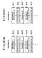
- FIGURE 15 is a block diagram showing a construction of a synchronous processing element 10c in a third embodiment.
- FIGURE 16 is a flowchart showing processes of the program A in the third embodiment.
- the synchronous processing element 10c in the third embodiment includes synchronous status registers 12a and 12b, synchronous mask registers 11a and 11b, synchronous receiving elements 15a and 15b, synchronous detecting elements 13a and 13b and synchronous indicating registers 14a and 14b.
- One group of elements and registers 11a, 12a, 13a, 14a, and 15a are employed for the synchronous processing of the program A, while the other group of elements and registers 11b, 12b, 13b, 14b, and 15b are for the synchronous processing of the program B.
- a synchronous status register 12a, a synchronous mask register 11a, a synchronous receiving element 15a, a synchronous detecting element 13a and a synchronous indicating register 14a are provided for executing the processes of the program A while being synchronized.
- a synchronous status register 12b, a synchronous mask register 11b, a synchronous receiving element 15b, a synchronous detecting element 13b and a synchronous indicating register 14b are provided for executing the processes of the program B while being synchronized.
- the synchronous status registers etc. are provided in pairs. Hence, the number of the processors provided in the third embodiment is one-half of the number of the processors provided in the first embodiment.
- the processors 1-0, 1-1, 1-2, 1-3 start executing the process k (step 302).
- Each of the processors 1-0, 1-1, 1-2, 1-3 in which the program A is being executed sets, when a status to take the synchronization on the program A is reached, "1" in the synchronous status register 12a (step 303).
- the synchronous status information "1" of the synchronous status register 12a is transmitted to the synchronizing broadcasting element 22 on the communication network 2 (step 304).
- the synchronous status information "1" is broadcast to all other processors from the synchronizing broadcasting element 22.
- the synchronous receiving elements 15a of the respective processors receive pieces of synchronous status information "1" of the synchronous status registers 12a of all the processors.
- the synchronous detecting element 13a performs a logic operation with respect to the synchronous status information of the synchronous receiving element 15a and the synchronization combination information of the synchronous mask register 11a, thereby detecting the synchronization (step 305). Note that if the synchronization is not detected, there is a waiting period for receiving the synchronous status information (step 306). It is next judged whether the value of the synchronous indicating register 14a is set to 1 or not (step 307). Note that the synchronous detecting element for setting "1" in the synchronous indicating register 14a is constructed the same as in FIGURE 9.
- the synchronous status information "0" of the synchronous status register 12a is transmitted to the synchronizing broadcasting element 22 on the network 2 (step 310).
- the synchronous status information "0" is broadcast to all other processors from the synchronizing broadcast 22.
- the synchronous receiving elements 15a of the respective processors receive pieces of synchronous status information "0" of the synchronous status registers 12a of all other processors.
- the synchronous detecting element 13a executes the logic operation with respect to the synchronous status information of the synchronous receiving element 15a and the synchronization combination information of the synchronous mask register 11a, thereby detecting the synchronization (step 311).
- the synchronous detecting element for setting "0" in the synchronous indicating register 14a is constructed the same as in FIGURE 10.
- the value of the synchronous indicating register 14a becomes "0"
- the next processing is consecutively proceeded to.
- the action returns to step 301.
- the processes from steps 301 ⁇ 314 are executed.
- the processes are executed in parallel by repeating the synchronization based on the synchronous status information "1" and the synchronization based on the synchronous status information "0".
- the program B is allocated to the processors 1-0, 1-1, 1-2, 1-3 absolutely independently of the action of the program A described above.
- a bit pattern "1111" is set in the synchronous mask registers 11b of the processors 1-0, 1-1, 1-2, 1-3.
- Parallel processing of the program B is also executed the same way as with the program A while taking the synchronization based on the synchronous status information "1" and the synchronization based on the synchronous status information "0".
- the synchronous processing element includes a plurality of the synchronous status registers, the synchronous mask registers, the synchronous indicating registers, etc.
- the plurality of user's parallel processing programs can be highly efficiently executed by a small number of processors.
- FIGURE 17 is a block diagram illustrating a construction of the synchronous processing element 10d in the fourth embodiment.
- the fourth embodiment has a construction in which a plurality of processes are executable. In the case of executing, for instance, only one process, however, this involves the use of one group of registers. The other group of registers are useless. Under such circumstances, the parallel processing programs are executed by switching over the plurality of processes and one process in accordance with the fourth embodiment.
- a synchronous processing element 10d in the fourth embodiment includes a synchronous status register 12a, a synchronous mask register 11a, a synchronous receiving element 15a, a synchronous detecting element 13a and a synchronous indicating register 14a.
- the synchronous processing element 10d further includes a synchronous status register 12b, a synchronous mask register 11b, a synchronous receiving element 15b, a synchronous detecting element 13b and a synchronous indicating register 14b.
- a synchronous side control register 18 accessed by the instruction processing element 8 is a 2-bit length register.
- the synchronous side control register 18 stores 2- or 1-process information for designating any one of two processes (two programs) or one process (one program) for one processor.
- the synchronous side control register 18 imparts the 2-or 1-process information to the synchronous status registers 12a, 12b, the synchronous mask registers 11a, 11b, the synchronous receiving elements 15a, 15b,the synchronous detecting elements 13a, 13b and the synchronous indicating registers 14a, 14b.
- FIGURE 18 shows an action flow of two processes by one processor.
- the instruction processing element 8 sets 2-process information "01" in the synchronous side control register 18.
- the synchronous status register 12a, the synchronous mask register 11a, the synchronous receiving element 15a, the synchronous detecting element 13a and the synchronous indicating register 14a execute the processes of the program A. These processes are executed while taking the synchronization on the basis of the 2-process information "01".
- the instruction processing element 8 performs an arithmetic operation A of the program A within one processor (step 401). Then, the synchronous processing element 10d executes synchronization A (step 402). The data transfer element 9 effects a transfer A of data of an arithmetic result to other processors (step 403). Further, the action proceeds to the next process, and steps 404, 405 are to be conducted.
- the synchronous status register 12b, the synchronous mask register 11b, the synchronous receiving element 15b, the synchronous detecting element 13b and the synchronous indicating register 14b execute the processes of the program B. These processes are executed while taking the synchronization on the basis of the 2-process information "10".
- the instruction processing element 8 performs an arithmetic operation B of the program B within one processor (step 411). Then, the synchronous processing element 10d executes synchronization B (step 412). The data transfer element 9 effects a transfer B of data of an arithmetic result to other processors (step 413). Further, the action proceeds to the next process, and steps 414, 415 are to be conducted. Namely, the 2-process actions are effected by one processor.
- FIGURE 19 shows an action flow of one process by one processor.
- one program C is divided into subprograms C1, C2 which are to be executed in parallel.
- One-process information "11" is set in the synchronous side control register 18.
- the synchronous status register 12a, the synchronous mask register 11a, the synchronous receiving element 15a, the synchronous detecting element 13a and the synchronous indicating register 14a execute the process of the subprogram C1. This process is executed while taking the synchronization on the basis of the 1-process information "11".
- the instruction processing element performs an arithmetic operation C1 of the subprogram C1 within one processor (step 421). Then, the synchronous processing element executes synchronization C1 (step 422). The data transfer element effects a transfer C1 of data of an arithmetic result to other processors (step 423). Further, the action proceeds to the next process, and steps 424, 425 are to be conducted.
- the synchronous status register 12b, the synchronous mask register 11b, the synchronous receiving element 15b, the synchronous detecting element 13b and the synchronous indicating register 14b execute while taking the synchronization on the basis of the 1-process information "11".
- the instruction processing element performs an arithmetic operation C2 of the subprogram C2 within one processor (step 431). Then, the synchronous processing element executes synchronization C2 (step 432). The data transfer element effects a transfer C2 of data of an arithmetic result to other processors (step 433). Further, the action proceeds to the next process, and steps 434, 435 are to be conducted. Namely, the 1-process actions are effected by one processor.
- the synchronous processing apparatus shown in the third embodiment described above comprises processors each provided with pairs of registers, etc.
- the broadcasting line through which the synchronous status information of each processor is broadcast is set per process.
- FIGURE 20 is a block diagram illustrating a construction of a synchronous processing element 10e in the fifth embodiment.
- the synchronous processing element 10e in the fifth embodiment includes, as in the case of the synchronous processing element 10c in the third embodiment, pairs of the registers, etc.
- the synchronous processing element 10e also includes two broadcasting lines 23a, 23b corresponding respectively to the synchronous receiving elements 15a, 15b.
- a mode circuit 19 is connected to the instruction processing element 8 and the synchronous receiving elements 15a, 15b.
- the mode circuit 19 is defined as a 1-bit length register in which 1-mode information "0" or 2-mode information "1" is set when switching on a power supply of a processor synchronous processing apparatus.
- the mode circuit 19 works to connect the synchronous broadcasting lines 23a, 23b to the synchronous receiving element 15a when the 1-mode information "0" is set.
- the mode circuit 19 further works to connect the synchronous broadcasting line 23a to the synchronous receiving element 15a in the case of the 2-mode information "1" as well as connecting the synchronous broadcasting line 23b to the synchronous receiving element 15b.
- FIGURE 21 is a diagram showing a data format of a 2-process mode on the synchronous broadcasting line in the fifth embodiment.
- FIGURE 22 is a diagram showing a data format of a 1-process mode on the synchronous broadcasting line in the fifth embodiment.
- the 2 processes are processed in parallel by use of a couple of synchronous status registers 11a, 11b.
- This parallel processing will be explained with reference to FIGURES 20 and 21.
- the instruction processing element 8 sets 2-mode information "1" in the mode circuit 19.
- the mode circuit 19 works to connect the synchronous broadcasting line 23a to the synchronous receiving element 15a and the synchronous broadcasting line 23b to the synchronous receiving element 15b.
- a header is broadcasted through the synchronous broadcasting line 23a. Further, a piece of synchronous status information a of the synchronous status register 12a is broadcast therethrough. In this parallel action, the header is broadcast via the synchronous broadcasting line 23b. Furthermore, a piece of synchronous status information b is broadcast via the same line.
- the synchronous receiving element 15a receives the synchronous status information a of the synchronous status register 12a.
- the synchronous receiving element 15b receives the synchronous status information b of the synchronous status register 11b. The two processes are thereby executable in parallel.
- the synchronous status information of the synchronous status register 12a is broadcast via the two synchronous broadcasting lines 23a, 23b.
- a piece of synchronous status information al is transmitted from the broadcasting line 23a, and, after a given time has elapsed, a piece of synchronous status information a2 is transmitted from the broadcasting line 23b. That is, the pieces of information are transmitted with a phase shift due to a serial bit.
- the synchronization can be taken based on the synchronous status information in which timings are matched in the two broadcasting lines 23a, 23b.
- the apparatus capable of executing the 2 processes in this manner is provided with the mode circuit 19 which can set the two modes, i.e., the 1- and 2-process modes.
- the mode circuit 19 sets the 1-process mode. Namely, the synchronous status information is transferred by use of the two broadcasting lines 23a, 23b during the 1-process mode. The synchronization can be therefore taken at a high speed, and the parallel processing programs are executable at a high efficiency.
- the synchronous status information is serially transferred in bits through the synchronous broadcasting lines.
- a 1-bit parity error may, however, be caused due to an influence of noises, etc. with respect to the synchronous status information on the synchronous broadcasting lines.
- the processor in which the parity error is detected is disconnected from the network 2, and hence the execution of the program is interrupted. If the execution of the program is interrupted due to such a non-serious error, the execution of the processing becomes inefficient.
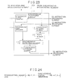
- FIGURE 23 is a block diagram illustrating a construction of a synchronous processing element 10f.
- FIGURE 24 shows a data format on the synchronous broadcasting line. As shown in FIGURE 24, the data such as a header, synchronous status information of the processors 1-0 ⁇ 1-7 and a parity P are transmitted in serial via the synchronous broadcasting line.
- the synchronous receiving element 15 is a register for receiving the synchronous status information which has been broadcast in 1-bit serial from the synchronous broadcasting element 22. At the same time, the synchronous receiving element 15 receives the 1-bit parity per 8 bits and hold these items of information. A parity error detecting element 20 checks whether or not an error exists in the 1-bit parity received per 8 bits by the synchronous receiving element 15.
- FIGURE 25 is a block diagram illustrating configurations of the parity error detecting element 20 and its peripheral portion. The operation of the sixth embodiment will be explained referring to FIGURES 23 and 25.
- a 1-bit length flip-flop (FF) 31 receives the synchronous status information broadcast in 1-bit serial via the synchronizing broadcasting line 23 from the synchronous broadcasting element 22.
- the synchronous status information is 1-bit information of "0" or "1". This synchronous status information is broadcasted via the synchronous broadcasting line to each processor. When this synchronous status information passes through the synchronous broadcasting line, it may happen that, for example, a bit "1" is changed into “0" due to outside noises.
- Parity error detecting element 20 checks whether or not an error is caused in the 8-bit synchronous status information received by synchronous receiving element 15 by use of the 1-bit parity bit P.
- FF32 adds a 1 parity bit to 8 bits of the synchronous status information.
- Parity checker 34 (PCHK) checks whether or not an error is produced in a tuple of 8 bits of synchronous status information and 1 parity bit, which is given by FF32. For instance, if a total sum of 8 bits of synchronous status information and 1 parity bit is to be an odd number parity checker 34 judges an error to exist if the given-by-FF32 total sum of 8 bits of synchronous status information and 1 parity bit is not an odd number.
- the parity error is detected when the data from the synchronous broadcasting line is such data that the content of synchronous indicating register 14 is not changed.
- the data sent from the synchronous broadcasting line is, for instance, "110000001".
- the 8 higher-order bits are the synchronous status information, while lowest-order bit is the parity bit.
- the total sum of bits having the "1" level is 3 bits, i.e., an odd number.
- the data from FF32 is "110000011".
- the total sum of "1" bits is 4 bits, i.e., an even number. Parity checker 34 therefore judges that there is an error.
- the error information from parity checker 34 is transferred via FF35, FF36 to FF37.
- FF37 informs instruction processing element 8 of system retaining ("SR") information indicating that the system is not interrupted.
- FF38 retains parity error information.
- parity checker 34 again detects the error, AND40 ANDs error information of parity checker 34 through FF35 and error information already stored in FF38.
- FF41 notifies instruction processing element 8 of system-down information with an AND output of AND40. In this case, the processor which detects the error is disconnected from network 2.
- a parity generator 42 modifies the parity bit "1" of the data "110000011” from FF32 to "0", thereby generating data "110000010".
- This data "110000010” is inputted via FF33 to AND43.
- AND43 ANDs the data "110000001” stored in synchronous mask register 11 and the above data "110000010” and outputs the result to synchronous indicating register 14 via FF44, FF45.
- parity generator 42 modifies the parity bit "0" of the data "110000000” from FF32 to "1", thereby generating data "110000001”.
- This data "110000001” is inputted via FF33 to AND43. AND43 ANDs the data "110000001” stored in synchronous mask register 11 and the above data "110000001” and outputs the result to synchronous indicating register 14 via FF44, FF45.
- the data "110000001” from FF33 is identical with the data "110000001” from synchronous mask register 11, and hence the value of synchronous indicating register 14 changes from “0” to "1". Note that the value of synchronous indicating register 14 reversely changes from “1” to "0” as the case may be.
- AND 39 ANDs the data from FF36, the data from synchronous indicating register 14 and the data from FFs 47a-47n through AND46. If the parity error is present, AND39 is turned ON and modifies instruction processing element 8 of the system-down information.
- the processing can be executed without interrupting the program, so that parallel processing of a program can be executed with high efficiency.
Applications Claiming Priority (3)
| Application Number | Priority Date | Filing Date | Title |
|---|---|---|---|
| JP33850292 | 1992-12-18 | ||
| JP338502/92 | 1992-12-18 | ||
| JP33850292A JP3285629B2 (ja) | 1992-12-18 | 1992-12-18 | 同期処理方法及び同期処理装置 |
Publications (2)
| Publication Number | Publication Date |
|---|---|
| EP0602906A1 EP0602906A1 (en) | 1994-06-22 |
| EP0602906B1 true EP0602906B1 (en) | 1999-06-09 |
Family
ID=18318765
Family Applications (1)
| Application Number | Title | Priority Date | Filing Date |
|---|---|---|---|
| EP93309957A Expired - Lifetime EP0602906B1 (en) | 1992-12-18 | 1993-12-10 | Synchronous processing method and apparatus for a plurality of processors executing a plurality of programs in parallel |
Country Status (4)
| Country | Link |
|---|---|
| US (1) | US5634071A (ja) |
| EP (1) | EP0602906B1 (ja) |
| JP (1) | JP3285629B2 (ja) |
| DE (1) | DE69325246T2 (ja) |
Cited By (1)
| Publication number | Priority date | Publication date | Assignee | Title |
|---|---|---|---|---|
| US11799947B2 (en) | 2009-12-10 | 2023-10-24 | Royal Bank Of Canada | Coordinated processing of data by networked computing resources |
Families Citing this family (16)
| Publication number | Priority date | Publication date | Assignee | Title |
|---|---|---|---|---|
| JP2552784B2 (ja) * | 1991-11-28 | 1996-11-13 | 富士通株式会社 | 並列データ処理制御方式 |
| JO1812B1 (en) † | 1993-10-15 | 1995-07-05 | ساسول كيميكال اندستريز ليمتد | Porous granules of ammonium nitrate |
| GB9606833D0 (en) * | 1996-03-30 | 1996-06-05 | Int Computers Ltd | Multi-processor system |
| US5958019A (en) * | 1996-07-01 | 1999-09-28 | Sun Microsystems, Inc. | Multiprocessing system configured to perform synchronization operations |
| US6067610A (en) * | 1996-07-29 | 2000-05-23 | Motorola, Inc. | Method and data processor for synchronizing multiple masters using multi-bit synchronization indicators |
| US6029204A (en) * | 1997-03-13 | 2000-02-22 | International Business Machines Corporation | Precise synchronization mechanism for SMP system buses using tagged snoop operations to avoid retries |
| US6314495B1 (en) * | 1998-01-07 | 2001-11-06 | International Business Machines Corporation | Method and apparatus for executing multiply-initiated, multiply-sourced variable delay system bus operations |
| CN1070625C (zh) * | 1998-01-15 | 2001-09-05 | 英业达股份有限公司 | 一种网络对打应用程序中的同步控制方法 |
| JP2000132529A (ja) * | 1998-10-23 | 2000-05-12 | Sony Corp | 並列処理装置、並列処理方法および記録媒体 |
| KR100394827B1 (ko) * | 1999-12-22 | 2003-08-21 | 엘지전자 주식회사 | 이동통신교환기의 프로세서 재시동을 위한 프로그램 및데이터 적재방법 |
| JP5273045B2 (ja) | 2007-06-20 | 2013-08-28 | 富士通株式会社 | バリア同期方法、装置、及びプロセッサ |
| US9940670B2 (en) | 2009-12-10 | 2018-04-10 | Royal Bank Of Canada | Synchronized processing of data by networked computing resources |
| US9979589B2 (en) | 2009-12-10 | 2018-05-22 | Royal Bank Of Canada | Coordinated processing of data by networked computing resources |
| US9959572B2 (en) | 2009-12-10 | 2018-05-01 | Royal Bank Of Canada | Coordinated processing of data by networked computing resources |
| CA3109739A1 (en) | 2009-12-10 | 2011-01-11 | Royal Bank Of Canada | Synchronized processing of data by networked computing resources |
| WO2012127534A1 (ja) * | 2011-03-23 | 2012-09-27 | 富士通株式会社 | バリア同期方法、バリア同期装置及び演算処理装置 |
Family Cites Families (6)
| Publication number | Priority date | Publication date | Assignee | Title |
|---|---|---|---|---|
| US5243698A (en) * | 1982-11-26 | 1993-09-07 | Inmos Limited | Microcomputer |
| JPS6345670A (ja) * | 1986-08-13 | 1988-02-26 | Hitachi Ltd | プロセツサ間同期装置 |
| JP2594979B2 (ja) * | 1987-10-23 | 1997-03-26 | 株式会社日立製作所 | マルチプロセツサシステム |
| JPH0630094B2 (ja) * | 1989-03-13 | 1994-04-20 | インターナショナル・ビジネス・マシーンズ・コーポレイション | マルチプロセツサ・システム |
| GB9019025D0 (en) * | 1990-08-31 | 1990-10-17 | Ncr Co | Work station having multiprocessing capability |
| DE69130630T2 (de) * | 1990-09-14 | 1999-09-09 | Hitachi Ltd | Synchrones Verfahren und Gerät für Prozessoren |
-
1992
- 1992-12-18 JP JP33850292A patent/JP3285629B2/ja not_active Expired - Fee Related
-
1993
- 1993-12-10 DE DE69325246T patent/DE69325246T2/de not_active Expired - Fee Related
- 1993-12-10 EP EP93309957A patent/EP0602906B1/en not_active Expired - Lifetime
-
1996
- 1996-02-15 US US08/601,705 patent/US5634071A/en not_active Expired - Lifetime
Cited By (1)
| Publication number | Priority date | Publication date | Assignee | Title |
|---|---|---|---|---|
| US11799947B2 (en) | 2009-12-10 | 2023-10-24 | Royal Bank Of Canada | Coordinated processing of data by networked computing resources |
Also Published As
| Publication number | Publication date |
|---|---|
| JP3285629B2 (ja) | 2002-05-27 |
| JPH06187303A (ja) | 1994-07-08 |
| US5634071A (en) | 1997-05-27 |
| DE69325246T2 (de) | 1999-09-30 |
| EP0602906A1 (en) | 1994-06-22 |
| DE69325246D1 (de) | 1999-07-15 |
Similar Documents
| Publication | Publication Date | Title |
|---|---|---|
| EP0602906B1 (en) | Synchronous processing method and apparatus for a plurality of processors executing a plurality of programs in parallel | |
| US5781775A (en) | Parallel process scheduling method in a parallel computer and a processing apparatus for a parallel computer | |
| US4972314A (en) | Data flow signal processor method and apparatus | |
| JPH07234842A (ja) | 並列データ処理システム | |
| US4641275A (en) | Vector processor having pair process mode and single process mode | |
| EP0460599B1 (en) | Massively parallel processor including queue-based message delivery system | |
| EP0601029B1 (en) | Massively parallel computer system including input/output arrangement | |
| Kartashev et al. | A multicomputer system with dynamic architecture | |
| EP0125044B1 (en) | Microcomputer with interprocess communication | |
| US4739472A (en) | Information processing device capable of rapidly processing instructions of different groups | |
| US5832261A (en) | Barrier synchronizing mechanism for a parallel data processing control system | |
| US20050086412A1 (en) | System and method for communicating between modules | |
| JPH0668053A (ja) | 並列計算機 | |
| JP3581419B2 (ja) | データ駆動型情報処理装置 | |
| JPH11110362A (ja) | 計算機間データ通信方法 | |
| US4809171A (en) | Concurrent processing of data operands | |
| EP0105125B1 (en) | Data processing system | |
| CN112994998A (zh) | 一种通讯节点、通讯方法、装置及电子设备 | |
| US11940940B2 (en) | External exchange connectivity | |
| JPH0981525A (ja) | 並列処理システム | |
| US11907725B2 (en) | Communication in a computer having multiple processors | |
| JPH07262142A (ja) | 並列処理制御方式 | |
| EP0107447B1 (en) | Computer data distributor | |
| JPH1027164A (ja) | 分散処理方法 | |
| JPH0520783B2 (ja) |
Legal Events
| Date | Code | Title | Description |
|---|---|---|---|
| PUAI | Public reference made under article 153(3) epc to a published international application that has entered the european phase |
Free format text: ORIGINAL CODE: 0009012 |
|
| AK | Designated contracting states |
Kind code of ref document: A1 Designated state(s): DE FR GB |
|
| 17P | Request for examination filed |
Effective date: 19940719 |
|
| 17Q | First examination report despatched |
Effective date: 19970917 |
|
| GRAG | Despatch of communication of intention to grant |
Free format text: ORIGINAL CODE: EPIDOS AGRA |
|
| GRAG | Despatch of communication of intention to grant |
Free format text: ORIGINAL CODE: EPIDOS AGRA |
|
| GRAH | Despatch of communication of intention to grant a patent |
Free format text: ORIGINAL CODE: EPIDOS IGRA |
|
| GRAH | Despatch of communication of intention to grant a patent |
Free format text: ORIGINAL CODE: EPIDOS IGRA |
|
| GRAA | (expected) grant |
Free format text: ORIGINAL CODE: 0009210 |
|
| AK | Designated contracting states |
Kind code of ref document: B1 Designated state(s): DE FR GB |
|
| REF | Corresponds to: |
Ref document number: 69325246 Country of ref document: DE Date of ref document: 19990715 |
|
| ET | Fr: translation filed | ||
| PLBE | No opposition filed within time limit |
Free format text: ORIGINAL CODE: 0009261 |
|
| STAA | Information on the status of an ep patent application or granted ep patent |
Free format text: STATUS: NO OPPOSITION FILED WITHIN TIME LIMIT |
|
| 26N | No opposition filed | ||
| REG | Reference to a national code |
Ref country code: GB Ref legal event code: IF02 |
|
| PGFP | Annual fee paid to national office [announced via postgrant information from national office to epo] |
Ref country code: GB Payment date: 20061206 Year of fee payment: 14 |
|
| PGFP | Annual fee paid to national office [announced via postgrant information from national office to epo] |
Ref country code: DE Payment date: 20061207 Year of fee payment: 14 |
|
| PGFP | Annual fee paid to national office [announced via postgrant information from national office to epo] |
Ref country code: FR Payment date: 20061208 Year of fee payment: 14 |
|
| GBPC | Gb: european patent ceased through non-payment of renewal fee |
Effective date: 20071210 |
|
| PG25 | Lapsed in a contracting state [announced via postgrant information from national office to epo] |
Ref country code: DE Free format text: LAPSE BECAUSE OF NON-PAYMENT OF DUE FEES Effective date: 20080701 |
|
| REG | Reference to a national code |
Ref country code: FR Ref legal event code: ST Effective date: 20081020 |
|
| PG25 | Lapsed in a contracting state [announced via postgrant information from national office to epo] |
Ref country code: GB Free format text: LAPSE BECAUSE OF NON-PAYMENT OF DUE FEES Effective date: 20071210 |
|
| PG25 | Lapsed in a contracting state [announced via postgrant information from national office to epo] |
Ref country code: FR Free format text: LAPSE BECAUSE OF NON-PAYMENT OF DUE FEES Effective date: 20071231 |