EP0601935B1 - Controlled delay circuit - Google Patents
Controlled delay circuit Download PDFInfo
- Publication number
- EP0601935B1 EP0601935B1 EP93402978A EP93402978A EP0601935B1 EP 0601935 B1 EP0601935 B1 EP 0601935B1 EP 93402978 A EP93402978 A EP 93402978A EP 93402978 A EP93402978 A EP 93402978A EP 0601935 B1 EP0601935 B1 EP 0601935B1
- Authority
- EP
- European Patent Office
- Prior art keywords
- current
- current source
- voltage
- delay
- signal
- Prior art date
- Legal status (The legal status is an assumption and is not a legal conclusion. Google has not performed a legal analysis and makes no representation as to the accuracy of the status listed.)
- Expired - Lifetime
Links
- 239000003990 capacitor Substances 0.000 claims description 58
- 230000005669 field effect Effects 0.000 claims description 14
- 230000003111 delayed effect Effects 0.000 claims description 10
- 230000001105 regulatory effect Effects 0.000 claims description 6
- 230000000295 complement effect Effects 0.000 claims description 5
- 230000001419 dependent effect Effects 0.000 claims 1
- 238000010586 diagram Methods 0.000 description 8
- 230000000630 rising effect Effects 0.000 description 4
- 238000010276 construction Methods 0.000 description 2
- 101150070189 CIN3 gene Proteins 0.000 description 1
- 101100508840 Daucus carota INV3 gene Proteins 0.000 description 1
- 238000007599 discharging Methods 0.000 description 1
- 238000005516 engineering process Methods 0.000 description 1
Images


Classifications
-
- H—ELECTRICITY
- H03—ELECTRONIC CIRCUITRY
- H03K—PULSE TECHNIQUE
- H03K5/00—Manipulating of pulses not covered by one of the other main groups of this subclass
-
- H—ELECTRICITY
- H03—ELECTRONIC CIRCUITRY
- H03K—PULSE TECHNIQUE
- H03K5/00—Manipulating of pulses not covered by one of the other main groups of this subclass
- H03K5/13—Arrangements having a single output and transforming input signals into pulses delivered at desired time intervals
- H03K5/133—Arrangements having a single output and transforming input signals into pulses delivered at desired time intervals using a chain of active delay devices
-
- H—ELECTRICITY
- H03—ELECTRONIC CIRCUITRY
- H03K—PULSE TECHNIQUE
- H03K5/00—Manipulating of pulses not covered by one of the other main groups of this subclass
- H03K5/01—Shaping pulses
- H03K5/04—Shaping pulses by increasing duration; by decreasing duration
-
- H—ELECTRICITY
- H03—ELECTRONIC CIRCUITRY
- H03K—PULSE TECHNIQUE
- H03K5/00—Manipulating of pulses not covered by one of the other main groups of this subclass
- H03K5/15—Arrangements in which pulses are delivered at different times at several outputs, i.e. pulse distributors
- H03K5/151—Arrangements in which pulses are delivered at different times at several outputs, i.e. pulse distributors with two complementary outputs
- H03K5/1515—Arrangements in which pulses are delivered at different times at several outputs, i.e. pulse distributors with two complementary outputs non-overlapping
Definitions
- the present invention relates to delay circuits and applies more particularly to a controlled delay circuit.
- CMOS circuits rests on a clock with two anti-overlap systems, such that the variations in the non-overlap values have an influence on the performance of such circuits.
- the object of the present invention is to create a delay device which is independent of the value of the power supply voltage, in order to reduce the variations in the anti-overlap value to a minimum, and to ensure good performance by the circuit despite significant variations in the power supply voltage.
- a delay circuit comprising a least one delay cell formed by a current source connected between the drains of two field-effect transistors whose gates are connected to each other in order to constitute the input of the cell, and an inverter linked to one or other of the terminals of the current source according to whether the delay is to affect the leading edge or the trailing edge of the signal to be delayed, a capacitor for defining a delay time proportional to the power supply voltage and inversely proportional to the current delivered by the current source, being connected between the input of the inverter and earth, characterized in that it furthermore comprises a circuit for regulating the current delivered by the current source in order to make it proportional to the power supply voltage of the circuit.
- this delay device depends only on the capacitance and on the ratio of the current mirror, which are kept well controlled in CMOS technology.
- Fig. 1 represents a means for generating a delay with the aid of a CMOS circuit. It takes the form of a circuit comprising a P-channel transistor PO, the gate of which is connected to the input of the circuit and the drain of which is linked to a current source I which is connected moreover to the drain of a N-channel transistor NO, the gate of which is connected to the input of the circuit and the source of which is connected to earth.
- a P-channel transistor PO the gate of which is connected to the input of the circuit and the drain of which is linked to a current source I which is connected moreover to the drain of a N-channel transistor NO, the gate of which is connected to the input of the circuit and the source of which is connected to earth.
- the drain of the transistor PO is furthermore connected to an inverter INV, the output of which forms the output of the circuit and the input of which is connected to a capacitor C linked to earth.
- the signal IN is applied to the input of the CMOS inverter produced by means of the transistor PO, of the transistor NO, of the current source I connected between the drain of the transistor PO and the drain of the transistor NO, of the capacitor C connected between the drain of the transistor PO and earth, and of the inverter INV proper, the input Vc of which is connected to the drain of the transistor PO.
- the abovementioned configuration makes it possible to delay the rising edge of the signal IN.
- the rising edge of the signal OUT of the inverter INV is delayed by a time Te with respect to the rising edge of the input signal IN by reason of the charge time of the capacitor C.
- an edge of the signal at the output OUT of the inverter INV is delayed by a value Te: where I is the current from the current source, k Vdd is the threshold voltage of the inverter and C is the value of the capacitance of the capacitor.
- the value of k depends mainly on the size ratio of the two transistors of the inverter.
- the proposed solution allows the current I to be made proportional to the power supply voltage Vdd and to the capacitance C.
- the diagram represented in Fig. 2 represents the means used to make the delay independent of the power supply voltage. It comprises mainly a differential amplifier AMPLO, one input of which is connected between two resistors R1, R1 of a voltage divider wired between the power supply voltage Vdd and earth,.
- AMPLO differential amplifier
- the other input of the differential amplifier AMPLO is connected to earth via three capacitors C1, Cu, Ci in parallel, a switch S1 being interposed between the capacitors C1 and Cu, a switch S2 being connected to the terminals of the capacitor C1 and a switch S3 being interposed between the capacitors Cu and Ci.
- the capacitor C1 has a capacitance which is markedly greater than that of the capacitor Cu, the ratio between these two capacitances being of the order of 10.
- the capacitor Ci also has a capacitance greater than that of the capacitor Cu.
- the switch S1 is controlled by the clock signal CK, while the switches S2 and S3 are both controlled by the signal CKB, which is the complement of the clock signal.
- the output of the amplifier AMPLO is connected to a current source PO wired between the power supply voltage Vdd and the terminal of the capacitor C1 linked to the switches S1 and S2.
- the principle consists in generating a current IO which is proportional to the power supply voltage Vdd and to the capacitance C.
- the capacitors C1 and Cu are put in parallel and connected to the current source IO.
- the capacitor C1 fixes the current delivered by the current source.
- the capacitor Cu establishes the voltage to be regulated.
- T is the period of the clock signal CK.
- the capacitor C1 is short-circuited and the capacitor Cu is connected in parallel to the capacitor Ci.
- the resultant voltage at the terminals of the capacitors Ci and Cu is compared with the value Vdd/2 or with any other appropriate fraction of Vdd, generated by means of the voltage divider with resistors R1, R2, by the differential amplifier AMPLO which generates an error voltage.
- This error voltage controls the value of IO which grows if the voltage at the terminals of the capacitor Ci is too small and increases if the voltage at the terminals Ci is too high. At equilibrium, the voltage at the terminals of the capacitor Ci is stabilized at Vdd/2, which means that there is no more charge redistribution between the capacitors Ci and Cu.
- the capacitor Cu has to be charged to the voltage Vdd/2 at the end of the clock signal CK.
- the charge at the terminals of the capacitor Cu is: when this gives:
- Fig. 3 represents an embodiment of the present invention for generating a signal, the positive edge of which is delayed with respect to the input signal.
- the circuit includes a circuit 1 produced from capacitors C1, Cu, Ci, from switches S1, S2, S3, from an amplifier AMPLO and from a transistor P1, which ensures production of a current proportional to the power supply voltage. This circuit is surrounded by the rectangle in long and short dashes 1 in Fig. 3.
- Switches S4 and S5 associated with capacitors C2 and Ci2 make it possible to keep, on the capacitor Ci2, the voltage present on the gate of the transistor P1 during the charging of the capacitors Cu + C1, and to generate, through a transistor P2, a precise copy of the current IO during the discharging of the capacitors Cu + C1.
- the circuit further includes a delay-cell forming circuit 2, represented by the rectangle in long and short dashes 2 in Fig. 3.
- Transistors N1 and N2 form a current mirror, N2 acting as current source in the delay cell 2. The rest of the circuit corresponds to the circuit of Fig. 1A.
- Fig. 4 represents a diagram of the waveforms of the signals at various points of the circuit of Fig. 3.
- Fig. 5 represents a first possible implementation of the device according to the invention with CMOS circuits, the construction of which is described by reference to Fig. 3.
- the circuit 1 for generating a current proportional to the power supply voltage includes the three capacitors C1, Ci and Cu of the circuit of Fig. 3.
- the three switches S1, S2 and S3 are physically represented respectively by MOS FET transistors NS1, NS2 and NS0, the source and the drain of which correspond to the fixed contacts and the gate corresponds to the movable contact.
- the gate of the transistor NS1 is connected to the clock signal CK, while the gates of the transistors NS2 and NS0 are connected to the signal CKB which is the complement of the clock signal CK.
- the differential amplifier AMPLO is physically represented by the transistors NA0, NA1, NA2 and PA0, PA1.
- the gate of the transistor NA1 is connected to the capacitor Ci.
- the source of this transistor is linked to the source-drain path of the transistor PA1 connected to the power supply voltage Vdd and the gate of which is connected to the drain.
- the drain of the transistor NA1 is connected to the drain of the transistor NA0, the gate of which is connected to the output of a voltage divider delivering a voltage
- the point common to the drain of the transistors NA0, NA1 is connected to the source-drain path of the transistor NA2 which receives a bias voltage Bias on its gate.
- the source of the transistor NA0 is connected to the source-drain path of a transistor PA0, the source of which is connected to the voltage Vdd and the gate of which is connected to the drain of the transistor PA0.
- the voltage divider delivering the voltage consists of two MOS FET transistors PA2, PA3 the source-drain paths of which are connected in series between the power supply voltage Vdd and earth and the gates of which are short-circuited with the drains.
- the output of the differential amplifier AMPLO is connected to the gate of the MOS FET transistor P1, the source-drain path of which is connected between the voltage Vdd and the capacitor C1. Furthermore, the gate of the transistor PA3 is connected to the gate of the transistor NA0.
- the gate of the transistor P1 is furthermore connected, via the source-drain path of a transistor NS3 physically representing the switch S4 of the circuit of Fig. 3, to one terminal of a capacitor C2, the other terminal of which is connected to earth.
- the gate of the transistor NS3 is connected to the clock signal CK.
- the capacitor C2 is connected to one terminal of a capacitor Ci2 via a transistor NS4 physically representing the switch S5 and the gate of which is controlled by the signal CKB.
- the capacitor Ci2 the other terminal of which is connected to earth, is moreover linked to the gate of a P-channel transistor P2, the source-drain path of which is connected between the power supply voltage Vdd and the source-drain path of a N-channel transistor N1, the source of which is connected to earth and the gate of which is short-circuited with the drain.
- the gate of the transistor N1 is, in its turn, linked to the gate of a transistor N2, the source-drain path of which is connected between the transistors P0 and N0 of the delay cell 2, those being connected in series between the power supply voltage Vdd and earth.
- the gates of the transistors P0 and N0 are connected together to receive the input signal IN to be delayed.
- the inverter INV and its associated capacitor C are connected to the source of the transistor N2 in order, in this case, to obtain a delay on the rising edge of the input signal IN.
- Fig. 6 represents a physical embodiment used to control the anti-overlap duration of a two-phase clock system used in a CMOS digital circuit.
- This circuit includes two delay cells 3, 4 the structure of which is analogous to that of the delay cell 2 of the circuit of Fig. 5 and the components of which are assigned the same references with the corresponding index 3 and 4.
- the circuit furthermore includes a circuit 5 for generating a current I proportional to the power supply voltage Vdd common to the two delay cells 3 and 4.
- the circuit 5 is identical at all points to the circuit 1 of Fig. 3, with the exception of the fact that it includes two transistors P23 and P24 associated respectively with transistors N13 and N14 of the corresponding current mirrors.
- circuit 5 applies the same current, proportional to the power supply voltage, to the two delay cells 3 and 4.
- the cell 3 is considered to be the "master” cell, while the cell 4 is the “slave” cell.
- the inputs of the two delay cells 3 and 4 are connected to the outputs of two dual-input NOR gates 6 and 7.
- the NOR gate 6 has one of its inputs connected to an input clock signal CLOCKIN while the NOR gate 7 receives the CLOCKIN signal, inverted by an inverter 8, on one of its inputs.
- the other input of the NOR gate 6 is connected to the output of the inverter INV4 of the delay cell 4 while the other input of the NOR gate 7 is connected to the output of the inverter INV3 of the delay cell 3.
- the delay cells 3 and 4 introduce a constant delay, independent of the variations in the power supply voltage of the circuit, the clock signals generated by the circuit, obtained from input signals in phase opposition, possess an anti-overlap duration which is constant in the presence of variations in the power supply voltage.
- the proposed circuit has been developed to control an anti-overlap, two-phase CMOS clock generator, but it may have other applications, either in the field of digital circuitry, or in that of analog circuits requiring the generation of delayed signals which are insensitive to variations in the power supply voltage.
Landscapes
- Physics & Mathematics (AREA)
- Nonlinear Science (AREA)
- Pulse Circuits (AREA)
- Electronic Switches (AREA)
Description
- The present invention relates to delay circuits and applies more particularly to a controlled delay circuit.
- The development of portable equipment, in particular in the field of telecommunications, is leading to the necessity for integrated circuits to be available operating within a wider range of power supply voltages (2.7 volts to 5.5 volts) than for conventional devices (5 volts +/- 10%).
- The construction of digital CMOS circuits rests on a clock with two anti-overlap systems, such that the variations in the non-overlap values have an influence on the performance of such circuits.
- The object of the present invention is to create a delay device which is independent of the value of the power supply voltage, in order to reduce the variations in the anti-overlap value to a minimum, and to ensure good performance by the circuit despite significant variations in the power supply voltage.
- Thus its object is a delay circuit comprising a least one delay cell formed by a current source connected between the drains of two field-effect transistors whose gates are connected to each other in order to constitute the input of the cell, and an inverter linked to one or other of the terminals of the current source according to whether the delay is to affect the leading edge or the trailing edge of the signal to be delayed, a capacitor for defining a delay time proportional to the power supply voltage and inversely proportional to the current delivered by the current source, being connected between the input of the inverter and earth, characterized in that it furthermore comprises a circuit for regulating the current delivered by the current source in order to make it proportional to the power supply voltage of the circuit.
- As it will be shown in the description which will follow, this delay device depends only on the capacitance and on the ratio of the current mirror, which are kept well controlled in CMOS technology.
- The invention will be better understood on reading the description which will follow, written with reference to the attached drawings which are given only by way of example and in which:
- Figs. 1A, 1B are electrical diagrams representing a known means for generating a delay with a CMOS circuit;
- Figs. 1C, 1D are signal diagrams at particular points of the circuits of Fig. 1A, 1B respectively;
- Fig. 2 is an electrical diagram of a device according to the invention for generating a current proportional to the power supply voltage;
- Fig. 3 is a more detailed electrical diagram of an embodiment of the delay device according to the invention;
- Fig. 4 is a diagram showing the signal waveforms at various points of the circuit of Fig. 3;
- Fig. 5 is an electrical diagram for implementing the circuit of Fig. 3 with the aid of CMOS devices;
- Fig. 6 represents the physical embodiment used to control the anti-overlap duration of a dual-phase clock system used in a CMOS digital circuit.
- Fig. 1 represents a means for generating a delay with the aid of a CMOS circuit. It takes the form of a circuit comprising a P-channel transistor PO, the gate of which is connected to the input of the circuit and the drain of which is linked to a current source I which is connected moreover to the drain of a N-channel transistor NO, the gate of which is connected to the input of the circuit and the source of which is connected to earth.
- The drain of the transistor PO is furthermore connected to an inverter INV, the output of which forms the output of the circuit and the input of which is connected to a capacitor C linked to earth.
- The signal IN is applied to the input of the CMOS inverter produced by means of the transistor PO, of the transistor NO, of the current source I connected between the drain of the transistor PO and the drain of the transistor NO, of the capacitor C connected between the drain of the transistor PO and earth, and of the inverter INV proper, the input Vc of which is connected to the drain of the transistor PO.
- As represented in Fig. 1C, the abovementioned configuration makes it possible to delay the rising edge of the signal IN. In fact, the rising edge of the signal OUT of the inverter INV is delayed by a time Te with respect to the rising edge of the input signal IN by reason of the charge time of the capacitor C.
- By connecting the capacitor C and the input of the inverter INV to the drain of the transistor NO as represented in Fig. 1B, the circuit otherwise being identical to that of Fig. 1A, it is the falling edge of the signal IN which is delayed. The signals of the circuit of Fig. 1D are represented in Fig. 1D.
- In both cases, an edge of the signal at the output OUT of the inverter INV is delayed by a value Te:where I is the current from the current source, k Vdd is the threshold voltage of the inverter and C is the value of the capacitance of the capacitor.

- The value of k depends mainly on the size ratio of the two transistors of the inverter.
- One drawback of this solution resides in the fact that the delay generated varies proportionally to the power supply voltage and to the capacitance C.
- The proposed solution allows the current I to be made proportional to the power supply voltage Vdd and to the capacitance C.
- The diagram represented in Fig. 2 represents the means used to make the delay independent of the power supply voltage. It comprises mainly a differential amplifier AMPLO, one input of which is connected between two resistors R1, R1 of a voltage divider wired between the power supply voltage Vdd and earth,.
- The other input of the differential amplifier AMPLO is connected to earth via three capacitors C1, Cu, Ci in parallel, a switch S1 being interposed between the capacitors C1 and Cu, a switch S2 being connected to the terminals of the capacitor C1 and a switch S3 being interposed between the capacitors Cu and Ci.
- The capacitor C1 has a capacitance which is markedly greater than that of the capacitor Cu, the ratio between these two capacitances being of the order of 10. The capacitor Ci also has a capacitance greater than that of the capacitor Cu.
- The switch S1 is controlled by the clock signal CK, while the switches S2 and S3 are both controlled by the signal CKB, which is the complement of the clock signal.
- The output of the amplifier AMPLO is connected to a current source PO wired between the power supply voltage Vdd and the terminal of the capacitor C1 linked to the switches S1 and S2.
- The principle consists in generating a current IO which is proportional to the power supply voltage Vdd and to the capacitance C. During the clock signal CK, the capacitors C1 and Cu are put in parallel and connected to the current source IO. The capacitor C1 fixes the current delivered by the current source. The capacitor Cu establishes the voltage to be regulated. At the end of the clock signal CK, the value of the voltage at the terminals of the abovementioned capacitors is:where T is the period of the clock signal CK. During the clock signal CKB, the capacitor C1 is short-circuited and the capacitor Cu is connected in parallel to the capacitor Ci. The resultant voltage at the terminals of the capacitors Ci and Cu is compared with the value Vdd/2 or with any other appropriate fraction of Vdd, generated by means of the voltage divider with resistors R1, R2, by the differential amplifier AMPLO which generates an error voltage.

- This error voltage controls the value of IO which grows if the voltage at the terminals of the capacitor Ci is too small and increases if the voltage at the terminals Ci is too high. At equilibrium, the voltage at the terminals of the capacitor Ci is stabilized at Vdd/2, which means that there is no more charge redistribution between the capacitors Ci and Cu.
- To this end, the capacitor Cu has to be charged to the voltage Vdd/2 at the end of the clock signal CK. As explained above, at the end of the clock signal CK, the charge at the terminals of the capacitor Cu is:when
 this gives: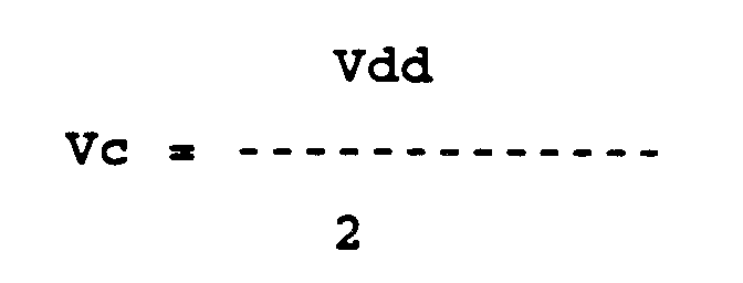
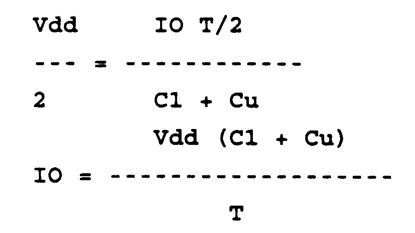
- The use of a copy of this current IO in the circuit generating a delayed signal gives:
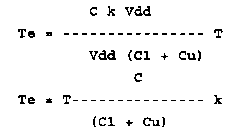
- The above relationship shows that the delay generated is now independent of the power supply voltage and depends only on the period of the clock, which is precise, on the capacitance ratio C/(C1 + Cu), the precision of which depends essentially on the care in production, and on the ratio k of the devices N and P forming the inverter.
- Fig. 3 represents an embodiment of the present invention for generating a signal, the positive edge of which is delayed with respect to the input signal. The circuit includes a
circuit 1 produced from capacitors C1, Cu, Ci, from switches S1, S2, S3, from an amplifier AMPLO and from a transistor P1, which ensures production of a current proportional to the power supply voltage. This circuit is surrounded by the rectangle in long andshort dashes 1 in Fig. 3. - Switches S4 and S5 associated with capacitors C2 and Ci2 make it possible to keep, on the capacitor Ci2, the voltage present on the gate of the transistor P1 during the charging of the capacitors Cu + C1, and to generate, through a transistor P2, a precise copy of the current IO during the discharging of the capacitors Cu + C1. The circuit further includes a delay-
cell forming circuit 2, represented by the rectangle in long andshort dashes 2 in Fig. 3. Transistors N1 and N2 form a current mirror, N2 acting as current source in thedelay cell 2. The rest of the circuit corresponds to the circuit of Fig. 1A. - Fig. 4 represents a diagram of the waveforms of the signals at various points of the circuit of Fig. 3.
- In this figure can be seen:
- the clock signal CK,
- the complement CKB of the clock signal,
- the voltage Vc1 on the capacitor C1,
- the voltage Vcu on the capacitor Cu,
- the voltage Vgsp1-Vdd applied to the pair of transistors N1, N2,
- the input signal IN,
- the voltage Vc at the terminals of the capacitor C of the delay circuit,
- the voltage OUT at the output of the delay circuit.
- Fig. 5 represents a first possible implementation of the device according to the invention with CMOS circuits, the construction of which is described by reference to Fig. 3.
- In this figure, the
circuit 1 for generating a current proportional to the power supply voltage includes the three capacitors C1, Ci and Cu of the circuit of Fig. 3. In contrast, the three switches S1, S2 and S3 are physically represented respectively by MOS FET transistors NS1, NS2 and NS0, the source and the drain of which correspond to the fixed contacts and the gate corresponds to the movable contact. - The gate of the transistor NS1 is connected to the clock signal CK, while the gates of the transistors NS2 and NS0 are connected to the signal CKB which is the complement of the clock signal CK.
- The differential amplifier AMPLO is physically represented by the transistors NA0, NA1, NA2 and PA0, PA1.
- The gate of the transistor NA1 is connected to the capacitor Ci. The source of this transistor is linked to the source-drain path of the transistor PA1 connected to the power supply voltage Vdd and the gate of which is connected to the drain.
- The drain of the transistor NA1 is connected to the drain of the transistor NA0, the gate of which is connected to the output of a voltage divider delivering a voltage

- The point common to the drain of the transistors NA0, NA1 is connected to the source-drain path of the transistor NA2 which receives a bias voltage Bias on its gate.
- The source of the transistor NA0 is connected to the source-drain path of a transistor PA0, the source of which is connected to the voltage Vdd and the gate of which is connected to the drain of the transistor PA0.
- The voltage divider delivering the voltageconsists of two MOS FET transistors PA2, PA3 the source-drain paths of which are connected in series between the power supply voltage Vdd and earth and the gates of which are short-circuited with the drains.

- The output of the differential amplifier AMPLO is connected to the gate of the MOS FET transistor P1, the source-drain path of which is connected between the voltage Vdd and the capacitor C1. Furthermore, the gate of the transistor PA3 is connected to the gate of the transistor NA0.
- The gate of the transistor P1 is furthermore connected, via the source-drain path of a transistor NS3 physically representing the switch S4 of the circuit of Fig. 3, to one terminal of a capacitor C2, the other terminal of which is connected to earth.
- The gate of the transistor NS3 is connected to the clock signal CK.
- The capacitor C2 is connected to one terminal of a capacitor Ci2 via a transistor NS4 physically representing the switch S5 and the gate of which is controlled by the signal CKB.
- The capacitor Ci2, the other terminal of which is connected to earth, is moreover linked to the gate of a P-channel transistor P2, the source-drain path of which is connected between the power supply voltage Vdd and the source-drain path of a N-channel transistor N1, the source of which is connected to earth and the gate of which is short-circuited with the drain.
- The gate of the transistor N1 is, in its turn, linked to the gate of a transistor N2, the source-drain path of which is connected between the transistors P0 and N0 of the
delay cell 2, those being connected in series between the power supply voltage Vdd and earth. - The gates of the transistors P0 and N0 are connected together to receive the input signal IN to be delayed.
- Finally, as already described by reference to Figs. 1A and 3, the inverter INV and its associated capacitor C are connected to the source of the transistor N2 in order, in this case, to obtain a delay on the rising edge of the input signal IN.
- Fig. 6 represents a physical embodiment used to control the anti-overlap duration of a two-phase clock system used in a CMOS digital circuit.
- This circuit includes two
delay cells delay cell 2 of the circuit of Fig. 5 and the components of which are assigned the same references with the correspondingindex - The circuit furthermore includes a
circuit 5 for generating a current I proportional to the power supply voltage Vdd common to the twodelay cells - The
circuit 5 is identical at all points to thecircuit 1 of Fig. 3, with the exception of the fact that it includes two transistors P23 and P24 associated respectively with transistors N13 and N14 of the corresponding current mirrors. - Hence the
circuit 5 applies the same current, proportional to the power supply voltage, to the twodelay cells - The
cell 3 is considered to be the "master" cell, while thecell 4 is the "slave" cell. - The inputs of the two
delay cells gates - The NOR
gate 6 has one of its inputs connected to an input clock signal CLOCKIN while the NORgate 7 receives the CLOCKIN signal, inverted by aninverter 8, on one of its inputs. - The other input of the NOR
gate 6 is connected to the output of the inverter INV4 of thedelay cell 4 while the other input of the NORgate 7 is connected to the output of the inverter INV3 of thedelay cell 3. - Having regard to that fact that the
delay cells - The proposed circuit has been developed to control an anti-overlap, two-phase CMOS clock generator, but it may have other applications, either in the field of digital circuitry, or in that of analog circuits requiring the generation of delayed signals which are insensitive to variations in the power supply voltage.
Claims (8)
- A signal delay circuit comprisingat least one delay cell, said at least one delay cell includingfirst and second field-effect transistors (PO, NO), each of said first and second field-effect transistors having a source, a drain, a channel between the source and drain, and a control gate overlying the channel, the first and second field-effect transistors being of opposite channel conductivity types,the control gates of said first and second field-effect transistors being connected to each other,an input terminal (IN) connected to a node in the connection between the control gates of said first and second field-effect transistors,a current source (I) having first and second terminals and being connected between the drains of said first and second field-effect transistors at said first and second terminals,an inverter (INV) having an input and an output, the input of said inverter being connected to one of said first and second terminals of said current source dependent upon whether the delay is to affect the leading edge or trailing edge of the signal to be delayed, anda capacitor (C) connected between the input of said inverter and ground, said capacitor defining a delay time (Te) for the signal to be delayed proportional to the power supply voltage and inversely proportional to the current delivered by said current source; characterized in thata control circuit (Ci,Cu,S1,S3,AMPLO,P1) is operably connected to said current source for dynamically regulating the current delivered by said current source so as to make the current dynamically proportional to the power supply voltage, such that the delay time remains approximately constant as the power supply voltage is varied.
- A signal delay circuit as set forth in Claim 1, further characterized in that said control circuit includesvoltage generating means (C1, Cu, S1) for generating a voltage (Vc) during a first clock signal (CK) having a predetermined relationship with the current delivered by said current source, andcomparison means (AMPLO, Ci, S2, S3) for comparing the voltage (Ve) linked to the current as delivered by said current source with a selected fraction (Vdd/2) of the power supply voltage during a second clock signal (CKB) complementary to the first clock signal,
said comparison means producing an error signal as an output for regulating said current source such that the voltage linked to the current delivered by said current source and the said fraction of the power supply voltage are substantially equal. - A signal delay circuit as set forth in Claim 2, further characterized in that said voltage generating means comprisesfirst and second capacitors (C1, Cu) connected in parallel to said current source,a clock-controlled switch (S1) interposed in the connection between said first and second capacitors and said current source and being responsive to the first clock signal (CK), and
said first capacitor (C1) of said voltage generating means fixing the current as delivered by said current source,
said second capacitor (Cu) of said voltage generating means being of smaller capacitance than said first capacitor and establishing the voltage (Vc) to be compared with said fraction (Vdd/2) of the power supply voltage. - A signal delay circuit as set forth in Claim 3, further characterized in that said comparison means for comparing the voltage (Vc) linked to the current as delivered by said current source with said fraction (Vdd/2) of the power supply voltage comprisesa third capacitor (Ci) connected in parallel with said second capacitor (Cu),a second clock-controlled switch (S3) interposed in the connection between said second and third capacitors and being responsive to the second clock signal (CKB),a third clock-controlled switch (S2) connected between said first capacitor (C1) and ground and being responsive to the second clock signal (CKB) for short-circuiting said first capacitor, anda differential amplifier (AMPLO) having first and second inputs for comparing said fraction (Vdd/2) of the power supply voltage with a voltage resulting from a redistribution of charge between said second capacitor (Cu) and said third capacitor (Ci) during the second clock signal (CKB).
- A signal delay circuit as set forth in any of Claims 1-4, further characterized in that said current source connected between the drains of said first and second field-effect transistors (PO, NO) includesthird and fourth field effect transistors (N1, N2) respectively having a source, a drain, a channel between the source and drain, and a control gate overlying the channel,the third and fourth field-effect transistors of said current source being arranged to define a current mirror in which the control gates of said third and fourth field-effect transistors included in said current source are connected together, andthe source and drain of said third field-effect transistor (N2) included in said current source being connected between the drains of said first and second field-effect transistors (PO, NO) of said at least one delay cell, and said control circuit having an output connected to said fourth field-effect transistor of said current source and providing a current proportional to the power supply voltage of the signal delay circuit to be copied by said current source.
- An anti-overlap two-phase clock generator comprising a signal delay circuit as set forth in any of Claims 1-5, including first and second delay cells (3, 4), characterized in that said control circuit (5) is common to said first and second delay cells and is respectively operably connected to the current source of each of said first and second delay cells for regulating the current delivered by the respective current source so as to make the current proportional to the power supply voltage,first and second logic means (6, 7) having respective first and second inputs and an output, said first and second logic means respectively receiving a clock input signal (CLOCKIN) and an inverted clock input signal at the first inputs thereof,the outputs of said first and second logic means being respectively connected to corresponding input terminals of said first and second delay cells, andthe output of said first delay cell being connected to the second input of said second logic means and the output of said second delay cell being connected to the second input of said first logic means.
- An anti-overlap two-phase clock generator as set forth in Claim 6, further characterized in that said first and second logic means are NOR gates (6, 7).
- An anti-overlap two-phase clock generator as set forth in either of Claims 6 or 7, further characterized in that said control circuit (5) common to said first and second delay cells (3, 4) includes voltage generating means (C1, Cu, S1) for generating a voltage during a first clock signal (CK) having a predetermined relationship with the current delivered by said current source of each of said first and second delay cells (3, 4), and comparison means (AMPLO, Ci, S2, S3) for comparing the voltage linked to the current as delivered by said current source of each of said first and second delay cells (3, 4) with a selected fraction (Vdd/2) of the power supply voltage during a second clock signal (CKB) complementary to the first clock signal,
said comparison means producing an error signal as an output for regulating said current sources of each of said first and second delay cells such that the voltage linked to the current as delivered by said current sources of each of said first and second delay cells and the said fraction of the power supply voltage are substantially equal.
Applications Claiming Priority (2)
| Application Number | Priority Date | Filing Date | Title |
|---|---|---|---|
| FR9214861A FR2699023B1 (en) | 1992-12-09 | 1992-12-09 | Controlled delay circuit. |
| FR9214861 | 1992-12-09 |
Publications (2)
| Publication Number | Publication Date |
|---|---|
| EP0601935A1 EP0601935A1 (en) | 1994-06-15 |
| EP0601935B1 true EP0601935B1 (en) | 2000-04-19 |
Family
ID=9436406
Family Applications (1)
| Application Number | Title | Priority Date | Filing Date |
|---|---|---|---|
| EP93402978A Expired - Lifetime EP0601935B1 (en) | 1992-12-09 | 1993-12-09 | Controlled delay circuit |
Country Status (8)
| Country | Link |
|---|---|
| US (1) | US5610546A (en) |
| EP (1) | EP0601935B1 (en) |
| JP (1) | JPH06232708A (en) |
| KR (1) | KR100338482B1 (en) |
| CA (1) | CA2110247A1 (en) |
| DE (1) | DE69328409T2 (en) |
| FR (1) | FR2699023B1 (en) |
| TW (1) | TW246756B (en) |
Cited By (1)
| Publication number | Priority date | Publication date | Assignee | Title |
|---|---|---|---|---|
| DE102006049233A1 (en) * | 2006-10-18 | 2008-04-24 | Texas Instruments Deutschland Gmbh | Overlapping signals generating circuit for controlling different elements in integrated circuits, has complementary MOS transistors, whose drains and taps between consecutive delay stages form knot, which provides one of overlapping signals |
Families Citing this family (20)
| Publication number | Priority date | Publication date | Assignee | Title |
|---|---|---|---|---|
| IT1283363B1 (en) * | 1996-07-30 | 1998-04-17 | Sgs Thomson Microelectronics | ASYMMETRIC AND PULSIVE DELAY NETWORK AND RELATIVE CONSTANT PULSE GENERATOR |
| US5748542A (en) * | 1996-12-13 | 1998-05-05 | Micron Technology, Inc. | Circuit and method for providing a substantially constant time delay over a range of supply voltages |
| JP3714762B2 (en) * | 1997-03-19 | 2005-11-09 | 富士通株式会社 | Delay circuit and semiconductor memory device |
| KR100453886B1 (en) * | 1997-07-29 | 2004-12-17 | 삼성전자주식회사 | Ring oscillator for generating clock signal with constant frequency regardless of supply voltage |
| US6067648A (en) * | 1998-03-02 | 2000-05-23 | Tanisys Technology, Inc. | Programmable pulse generator |
| US6307417B1 (en) | 1999-08-24 | 2001-10-23 | Robert J. Proebsting | Integrated circuit output buffers having reduced power consumption requirements and methods of operating same |
| US6356132B1 (en) | 2000-01-31 | 2002-03-12 | Agere Systems Guardian Corp. | Programmable delay cell |
| US6348827B1 (en) * | 2000-02-10 | 2002-02-19 | International Business Machines Corporation | Programmable delay element and synchronous DRAM using the same |
| US6549042B2 (en) | 2000-06-23 | 2003-04-15 | Integrated Device Technology, Inc. | Complementary data line driver circuits with conditional charge recycling capability that may be used in random access and content addressable memory devices and method of operating same |
| US7019576B1 (en) * | 2003-03-24 | 2006-03-28 | Cypress Semiconductor Corporation | Delay circuit that scales with clock cycle time |
| KR101005156B1 (en) * | 2003-05-30 | 2011-01-04 | 주식회사 하이닉스반도체 | Delay circuit |
| JP2006041175A (en) * | 2004-07-27 | 2006-02-09 | Toshiba Corp | Semiconductor integrated circuit device |
| JP2006352398A (en) * | 2005-06-15 | 2006-12-28 | Sanyo Electric Co Ltd | Delay circuit |
| JP4810132B2 (en) * | 2005-06-15 | 2011-11-09 | 三洋電機株式会社 | Delay circuit and ripple converter |
| US7705600B1 (en) | 2006-02-13 | 2010-04-27 | Cypress Semiconductor Corporation | Voltage stress testing of core blocks and regulator transistors |
| JP5224942B2 (en) * | 2008-06-30 | 2013-07-03 | キヤノン株式会社 | Solid-state imaging device |
| JP5389524B2 (en) * | 2009-05-14 | 2014-01-15 | セミコンダクター・コンポーネンツ・インダストリーズ・リミテッド・ライアビリティ・カンパニー | Delay circuit |
| JP2010273186A (en) * | 2009-05-22 | 2010-12-02 | Renesas Electronics Corp | Delay circuit |
| JP5967362B2 (en) * | 2012-06-29 | 2016-08-10 | セイコーNpc株式会社 | Delay circuit |
| JP7727164B2 (en) * | 2020-02-17 | 2025-08-21 | ミツミ電機株式会社 | Pulse signal transmission circuit |
Family Cites Families (11)
| Publication number | Priority date | Publication date | Assignee | Title |
|---|---|---|---|---|
| US4704547A (en) * | 1984-12-10 | 1987-11-03 | American Telephone And Telegraph Company, At&T Bell Laboratories | IGFET gating circuit having reduced electric field degradation |
| US4617477A (en) * | 1985-05-21 | 1986-10-14 | At&T Bell Laboratories | Symmetrical output complementary buffer |
| JPS62180607A (en) * | 1986-02-04 | 1987-08-07 | Fujitsu Ltd | Semiconductor integrated circuit |
| JP2681972B2 (en) * | 1988-02-26 | 1997-11-26 | 日本電気株式会社 | Master slice type semiconductor integrated circuit |
| US5068553A (en) * | 1988-10-31 | 1991-11-26 | Texas Instruments Incorporated | Delay stage with reduced Vdd dependence |
| US5081380A (en) * | 1989-10-16 | 1992-01-14 | Advanced Micro Devices, Inc. | Temperature self-compensated time delay circuits |
| DE4004135A1 (en) * | 1990-02-10 | 1991-08-14 | Thomson Brandt Gmbh | FREQUENCY COMPENSATED CIRCUIT |
| US5117130A (en) * | 1990-06-01 | 1992-05-26 | At&T Bell Laboratories | Integrated circuits which compensate for local conditions |
| US5066868A (en) * | 1990-08-13 | 1991-11-19 | Thomson Consumer Electronics, Inc. | Apparatus for generating phase shifted clock signals |
| KR940005004B1 (en) * | 1991-03-21 | 1994-06-09 | 삼성전자 주식회사 | Signal delay circuit |
| US5214320A (en) * | 1992-06-12 | 1993-05-25 | Smos Systems, Inc. | System and method for reducing ground bounce in integrated circuit output buffers |
-
1992
- 1992-12-09 FR FR9214861A patent/FR2699023B1/en not_active Expired - Fee Related
-
1993
- 1993-11-29 CA CA002110247A patent/CA2110247A1/en not_active Abandoned
- 1993-12-08 JP JP5308161A patent/JPH06232708A/en active Pending
- 1993-12-09 US US08/164,606 patent/US5610546A/en not_active Expired - Lifetime
- 1993-12-09 KR KR1019930027069A patent/KR100338482B1/en not_active Expired - Fee Related
- 1993-12-09 DE DE69328409T patent/DE69328409T2/en not_active Expired - Fee Related
- 1993-12-09 EP EP93402978A patent/EP0601935B1/en not_active Expired - Lifetime
-
1994
- 1994-03-04 TW TW083101877A patent/TW246756B/zh not_active IP Right Cessation
Cited By (2)
| Publication number | Priority date | Publication date | Assignee | Title |
|---|---|---|---|---|
| DE102006049233A1 (en) * | 2006-10-18 | 2008-04-24 | Texas Instruments Deutschland Gmbh | Overlapping signals generating circuit for controlling different elements in integrated circuits, has complementary MOS transistors, whose drains and taps between consecutive delay stages form knot, which provides one of overlapping signals |
| DE102006049233B4 (en) * | 2006-10-18 | 2008-06-26 | Texas Instruments Deutschland Gmbh | Circuit for generating overlapping signals |
Also Published As
| Publication number | Publication date |
|---|---|
| CA2110247A1 (en) | 1994-06-10 |
| US5610546A (en) | 1997-03-11 |
| FR2699023A1 (en) | 1994-06-10 |
| KR940017156A (en) | 1994-07-26 |
| JPH06232708A (en) | 1994-08-19 |
| KR100338482B1 (en) | 2002-08-21 |
| DE69328409T2 (en) | 2000-09-21 |
| FR2699023B1 (en) | 1995-02-24 |
| TW246756B (en) | 1995-05-01 |
| DE69328409D1 (en) | 2000-05-25 |
| EP0601935A1 (en) | 1994-06-15 |
Similar Documents
| Publication | Publication Date | Title |
|---|---|---|
| US5610546A (en) | Controlled delay circuit | |
| US5051630A (en) | Accurate delay generator having a compensation feature for power supply voltage and semiconductor process variations | |
| US4675617A (en) | Stable voltage controlled oscillator | |
| US4395774A (en) | Low power CMOS frequency divider | |
| EP0282725A1 (en) | CMOS reference voltage generator device | |
| US4581545A (en) | Schmitt trigger circuit | |
| US5331322A (en) | Current cell for digital-to-analog converter | |
| JPS62219813A (en) | Mosfet integrated delay circuit for digital signal | |
| JPH10256884A5 (en) | ||
| JPH10240849A (en) | Integrator and neural network synapse using current mirror with low voltage MOSFET | |
| GB2047492A (en) | Complementary transistor circuit | |
| JP2000013205A (en) | Complementary signal generation circuit device | |
| US5689205A (en) | Switched current differentiator | |
| JPH0399516A (en) | Level converting circuit | |
| JPH04115622A (en) | Current mirror type amplifier circuit and driving method therefor | |
| JPH07113862B2 (en) | Reference voltage generation circuit | |
| US5537063A (en) | CMOS logic circuit with plural inputs | |
| JPH0691462B2 (en) | Analog counter circuit | |
| JP2784262B2 (en) | Voltage comparator | |
| JPH06101650B2 (en) | Semiconductor integrated circuit device | |
| JPH10116309A (en) | Automatic adjustment operating point adjustment device in amplifier circuit having neuron MOS transistor | |
| KR0163774B1 (en) | Phase differential circuit having high synchronicity | |
| KR100230819B1 (en) | Variable delay circuit using constant current source | |
| JP2891832B2 (en) | LCD driver circuit | |
| JP3245914B2 (en) | Differential voltage comparison circuit |
Legal Events
| Date | Code | Title | Description |
|---|---|---|---|
| PUAI | Public reference made under article 153(3) epc to a published international application that has entered the european phase |
Free format text: ORIGINAL CODE: 0009012 |
|
| AK | Designated contracting states |
Kind code of ref document: A1 Designated state(s): DE ES FR GB IT NL SE |
|
| 17P | Request for examination filed |
Effective date: 19941207 |
|
| 17Q | First examination report despatched |
Effective date: 19960812 |
|
| GRAG | Despatch of communication of intention to grant |
Free format text: ORIGINAL CODE: EPIDOS AGRA |
|
| GRAG | Despatch of communication of intention to grant |
Free format text: ORIGINAL CODE: EPIDOS AGRA |
|
| GRAH | Despatch of communication of intention to grant a patent |
Free format text: ORIGINAL CODE: EPIDOS IGRA |
|
| GRAH | Despatch of communication of intention to grant a patent |
Free format text: ORIGINAL CODE: EPIDOS IGRA |
|
| GRAA | (expected) grant |
Free format text: ORIGINAL CODE: 0009210 |
|
| ITF | It: translation for a ep patent filed | ||
| AK | Designated contracting states |
Kind code of ref document: B1 Designated state(s): DE ES FR GB IT NL SE |
|
| PG25 | Lapsed in a contracting state [announced via postgrant information from national office to epo] |
Ref country code: ES Free format text: THE PATENT HAS BEEN ANNULLED BY A DECISION OF A NATIONAL AUTHORITY Effective date: 20000419 |
|
| REF | Corresponds to: |
Ref document number: 69328409 Country of ref document: DE Date of ref document: 20000525 |
|
| PG25 | Lapsed in a contracting state [announced via postgrant information from national office to epo] |
Ref country code: SE Free format text: LAPSE BECAUSE OF FAILURE TO SUBMIT A TRANSLATION OF THE DESCRIPTION OR TO PAY THE FEE WITHIN THE PRESCRIBED TIME-LIMIT Effective date: 20000719 |
|
| ET | Fr: translation filed | ||
| PLBE | No opposition filed within time limit |
Free format text: ORIGINAL CODE: 0009261 |
|
| STAA | Information on the status of an ep patent application or granted ep patent |
Free format text: STATUS: NO OPPOSITION FILED WITHIN TIME LIMIT |
|
| 26N | No opposition filed | ||
| PG25 | Lapsed in a contracting state [announced via postgrant information from national office to epo] |
Ref country code: NL Free format text: LAPSE BECAUSE OF NON-PAYMENT OF DUE FEES Effective date: 20010701 |
|
| NLV4 | Nl: lapsed or anulled due to non-payment of the annual fee |
Effective date: 20010701 |
|
| REG | Reference to a national code |
Ref country code: GB Ref legal event code: IF02 |
|
| PGFP | Annual fee paid to national office [announced via postgrant information from national office to epo] |
Ref country code: IT Payment date: 20061231 Year of fee payment: 14 |
|
| PGFP | Annual fee paid to national office [announced via postgrant information from national office to epo] |
Ref country code: FR Payment date: 20081205 Year of fee payment: 16 |
|
| PGFP | Annual fee paid to national office [announced via postgrant information from national office to epo] |
Ref country code: DE Payment date: 20081230 Year of fee payment: 16 |
|
| PG25 | Lapsed in a contracting state [announced via postgrant information from national office to epo] |
Ref country code: IT Free format text: LAPSE BECAUSE OF NON-PAYMENT OF DUE FEES Effective date: 20071209 |
|
| PGFP | Annual fee paid to national office [announced via postgrant information from national office to epo] |
Ref country code: GB Payment date: 20091106 Year of fee payment: 17 |
|
| REG | Reference to a national code |
Ref country code: FR Ref legal event code: ST Effective date: 20100831 |
|
| PG25 | Lapsed in a contracting state [announced via postgrant information from national office to epo] |
Ref country code: FR Free format text: LAPSE BECAUSE OF NON-PAYMENT OF DUE FEES Effective date: 20091231 |
|
| PG25 | Lapsed in a contracting state [announced via postgrant information from national office to epo] |
Ref country code: DE Free format text: LAPSE BECAUSE OF NON-PAYMENT OF DUE FEES Effective date: 20100701 |
|
| GBPC | Gb: european patent ceased through non-payment of renewal fee |
Effective date: 20101209 |
|
| PG25 | Lapsed in a contracting state [announced via postgrant information from national office to epo] |
Ref country code: GB Free format text: LAPSE BECAUSE OF NON-PAYMENT OF DUE FEES Effective date: 20101209 |