EP0601895B1 - Method for forming an orientation film - Google Patents
Method for forming an orientation film Download PDFInfo
- Publication number
- EP0601895B1 EP0601895B1 EP93310040A EP93310040A EP0601895B1 EP 0601895 B1 EP0601895 B1 EP 0601895B1 EP 93310040 A EP93310040 A EP 93310040A EP 93310040 A EP93310040 A EP 93310040A EP 0601895 B1 EP0601895 B1 EP 0601895B1
- Authority
- EP
- European Patent Office
- Prior art keywords
- liquid crystal
- coupling agent
- organic compound
- silane coupling
- mixture
- Prior art date
- Legal status (The legal status is an assumption and is not a legal conclusion. Google has not performed a legal analysis and makes no representation as to the accuracy of the status listed.)
- Expired - Lifetime
Links
Images


Classifications
-
- G—PHYSICS
- G02—OPTICS
- G02F—OPTICAL DEVICES OR ARRANGEMENTS FOR THE CONTROL OF LIGHT BY MODIFICATION OF THE OPTICAL PROPERTIES OF THE MEDIA OF THE ELEMENTS INVOLVED THEREIN; NON-LINEAR OPTICS; FREQUENCY-CHANGING OF LIGHT; OPTICAL LOGIC ELEMENTS; OPTICAL ANALOGUE/DIGITAL CONVERTERS
- G02F1/00—Devices or arrangements for the control of the intensity, colour, phase, polarisation or direction of light arriving from an independent light source, e.g. switching, gating or modulating; Non-linear optics
- G02F1/01—Devices or arrangements for the control of the intensity, colour, phase, polarisation or direction of light arriving from an independent light source, e.g. switching, gating or modulating; Non-linear optics for the control of the intensity, phase, polarisation or colour
- G02F1/13—Devices or arrangements for the control of the intensity, colour, phase, polarisation or direction of light arriving from an independent light source, e.g. switching, gating or modulating; Non-linear optics for the control of the intensity, phase, polarisation or colour based on liquid crystals, e.g. single liquid crystal display cells
- G02F1/133—Constructional arrangements; Operation of liquid crystal cells; Circuit arrangements
- G02F1/1333—Constructional arrangements; Manufacturing methods
- G02F1/1337—Surface-induced orientation of the liquid crystal molecules, e.g. by alignment layers
- G02F1/133711—Surface-induced orientation of the liquid crystal molecules, e.g. by alignment layers by organic films, e.g. polymeric films
- G02F1/133719—Surface-induced orientation of the liquid crystal molecules, e.g. by alignment layers by organic films, e.g. polymeric films with coupling agent molecules, e.g. silane
-
- C—CHEMISTRY; METALLURGY
- C09—DYES; PAINTS; POLISHES; NATURAL RESINS; ADHESIVES; COMPOSITIONS NOT OTHERWISE PROVIDED FOR; APPLICATIONS OF MATERIALS NOT OTHERWISE PROVIDED FOR
- C09K—MATERIALS FOR MISCELLANEOUS APPLICATIONS, NOT PROVIDED FOR ELSEWHERE
- C09K2323/00—Functional layers of liquid crystal optical display excluding electroactive liquid crystal layer characterised by chemical composition
- C09K2323/05—Bonding or intermediate layer characterised by chemical composition, e.g. sealant or spacer
- C09K2323/053—Organic silicon compound, e.g. organosilicon
Definitions
- the present invention relates to a method for forming an orientation film wherein a mixture of a liquid crystal compound and an organic compound which is oriented to a certain direction by utilizing orientation of the liquid crystal compound to the certain direction caused by magnetic field or voltage application is coupled to a silane coupling agent chemically adsorbed on a substrate surface.
- a liquid crystal display device is manufactured in a manner comprising the following steps:
- Transparent stripe-shaped electrodes made of a material such as ITO are formed on a transparent substrate made of a material such as glass, whereafter an orientation film is formed thereon. Then the two transparent substrates are disposed opposite to each other so that cross portions of the transparent electrodes are arranged in a matrix form.
- a spacer is disposed between the peripheral portions of both the substrates in order to provide a gap therebetween and the peripheral portions of both the substrates and the spacer are bonded with an adhesive agent.
- a liquid crystal is injected through an inlet into the gap and the inlet is sealed, whereby a liquid crystal device is formed.
- a polarization plate is disposed on the both sides of the liquid crystal device so that polarization axes through both the sides thereof make a right angle with each other.
- a liquid crystal display device which functions as a display device is completed by backlighting from one or both the sides thereof and applying a voltage thereto. Namely, displaying is performed by utilizing a character that when a voltage is applied to the liquid crystal device, an orientation phase of liquid crystal molecules varies, which results in variation of a transmitted light quantity.
- the uniform orientation depends on the use of an orientation film.
- an orientation film There are found several methods of forming an orientation film. For instance, in the rubbing method, a high molecular weight film of polyimide, polyvinyl alcohol or the like is applied on a substrate having electrodes thereon by use of a spinner. Thereafter the surface of the high molecular weight film is rotationally rubbed toward a certain direction with a roller wrapped with a cloth made of nylon. As a result of this process, distortion anisotropy is provided, which makes it possible to form an orientation film wherein the longitudinal axes of liquid crystal molecules are aligned with the rubbing direction.
- a method for forming a monomolecule adsorption film made of a silane coupling agent disclosed in Japanese Unexamined Patent Publications JP-A 66-7913 and JP-A 66-186818 is well known.
- this method are utilized several kinds of silane coupling agents which have a normal carbon chain, and a monochloro or trichloro silane group at one end thereof which is to be bonded on a substrate having electrodes, or have a compound at one end thereof whose structure is similar to that of a liquid crystal molecule to be injected into a liquid crystal device.
- These silane coupling agents are applied to the substrate with electrodes in order to be adsorbed on the entire surface of the substrate by a chemical adsorption method, whereby a monomolecule adsorption film made of the silane coupling agent is formed.
- a mixture of silane coupling agents with different lengths of normal carbon chains is employed to control a pretilt angle of a liquid crystal molecule.
- the rubbing method is an easy method of rubbing the surface of the polymer film with a cloth wrapping around a roller.
- the method is widely employed in industries due to the excellent mass productivity and high reliability thereof, but it has several disadvantages as follows.
- Electrostatic break down might occur in a thin film transistor for driving due to static electricity caused by rubbing with the cloth in the case of an active matrix type of liquid crystal device in which a MOS-FET is integrated. Further, the non-uniform thickness of the substrate, abrasion of the rubbing cloth or rubbing cloth dusts deposited on the polymer film causes non-uniformity of the rubbing intensity, which might also result in non-uniform orientation.
- a method without rubbing has been investigated in order to eliminate these disadvantages and a chemical adsorption method of a silane coupling agent has been proposed.
- a pretilt angle can be controlled by varying a mixing ratio of these silane coupling agents.
- the orientation direction of the mixture of the silane coupling agents is not controlled also in this case and therefore it is necessary to control the orientation direction of the mixture of the silane coupling agents in a manner such as rubbing, on or after the formation of a monomolecular adsorption film, in order to orient a liquid crystal to a certain direction.
- EP-A-0261712 discloses a method of forming an orientation layer in which a film of a liquid crystalline monomer is provided, the monomer is oriented in a magnetic or electric field at a given angle, and is then polymerised, e.g. by exposure to actinic light.
- the invention thus provides a method of forming an orientation film in situ with a liquid crystal comprising the following steps:
- the invention presents in one preferred option a first method for forming an orientation film comprising: a first step wherein a silane coupling agent is chemically adsorbed on a substrate surface, and a second step wherein an organic compound is coupled with the silane coupling agent in such a manner such that while a magnetic field is applied in a certain direction to a mixture of a liquid crystal compound being in a liquid crystal phase when heated and the organic compound with a functional group to be coupled with the silane coupling agent,
- the second step it is preferable in the second step to firstly apply the magnetic field to the mixture, and furthermore it is more preferable to heat after the substrate has been dipped.
- the invention presents in a second preferred option a second method for forming an orientation film comprising: a first step wherein a silane coupling agent is chemically adsorbed on a substrate surface, and a second step wherein an organic compound is coupled with the silane coupling agent in a certain direction in a manner that while a voltage is applied in a certain direction to a mixture of a liquid crystal compound being in a liquid crystal phase when heated and the organic compound with a functional group to be coupled with the silane coupling agent, the substrate is dipped to be directed to a certain direction relative to the direction of the voltage application and the mixture is heated up to a temperature whereat a reaction between the silane coupling agent and the organic compound begins. It is preferable in the second step to utilize a substrate with a plurality of stripe-shaped electrodes arranged parallel to each other and to apply a voltage to the mixture so that the polarities between the neighboring electrodes are different.
- the silane coupling agent is that with an epoxide at one end and the organic compound is that with at least one hydroxyl or amino group, or the coupling agent is that with a vinyl group at one end and the organic compound is that with at least one amino group.
- the manufacturing method of the liquid crystal device of the invention is characterized in that the two substrates on which an orientation film is formed are disposed opposite to each other and joined through a spacer and then a gap between the substrates is filled with a liquid crystal.
- An organic compound is oriented to a certain direction in a magnetic or electrical field by a liquid crystal for orientation and is coupled with a silane coupling agent. That makes it possible to control the orientation direction of the liquid crystal for display and uniformly orient the liquid crystal for display to any direction on a horizontal plane. Furthermore, the electrostatic breakdown of a thin film transistor, dusts deposition, and non-uniform orientation which are observed in the rubbing process are reduced.
- the orientation direction of the organic compound i.e. the orientation direction of the liquid crystal for display
- the relationship between the direction of voltage application and the orientation direction of longitudinal molecular axes of the liquid crystal for orientation and the organic compound depends on the dielectric anisotropy of the liquid crystal used for orientation. More specifically, when the dielectric anisotropy is positive, the direction of the voltage application and the orientation direction of the longitudinal molecular axes of the organic compound and the liquid crystal for orientation are identical. On the other hand, when the dielectric anisotropy is negative, the directi-on of the voltage application makes a right angle with the orientation direction of the longer molecular axis of the liquid crystal for orientation, namely of the organic compound.
- the direction of the magnetic field is the same as the orientation direction of the longer molecular axis of the organic compound and the liquid crystal for orientation.
- one molecule of one silane coupling agent is coupled with one molecule of the organic compound.
- two molecules of the silane coupling agent are coupled with one molecule of the organic compound.
- the coupling is caused by the reaction between the functional groups belonging to the organic compound and to the silane coupling agent, respectively.
- the combination of the functional group of the silane coupling agent and that of the organic compound is selected taking account of that the organic compound contributes to form an uniform mixture without negative effect on the reactivity and on the liquid crystal for orientation.
- a silane coupling agent with an epoxide is suitable for an organic compound with a hydroxyl or amino group and a silane coupling agent with a vinyl group is suitable for an organic compound with an amino group.
- a silane coupling agent with an epoxide is coupled with an organic compound with a hydroxyl or amino group, it is known as the coupling mechanism that a ring of epoxide is opened and coupling of the epoxide group with the hydroxyl or amino group occurs.
- a silane coupling agent with a vinyl group is coupled with an organic compound with an amino group, the coupling therebetween is caused by bonding of the amino group with the vinyl group due to Michell addition reaction.
- the stability of the orientation film it is preferred in view of the stability of the orientation film that a lot of functional groups such as hydroxyl group and amino group which react with the silane coupling agent are contained in the organic compound.
- an organic compound as shown in the following structural formula, with two functional groups positioned nearly at both longitudinal ends of the organic compound molecule is employed, the stability of the orientation film is secured because both the ends of the organic compound molecules are fixed by coupling with a silane coupling agent.
- the stability of the orientation film is secured to a certain degree provided that the employed organic compound includes a functional group such as hydroxyl group and amino group nearby the longitudinal center of the molecule thereof.
- a length of the molecule of the silane coupling agent is preferred to be shorter in view of stability of the orientation film.
- Examples of each substance shown in the following structural formulas are preferable, considering that the organic compound should form a homogeneous mixture without negative effect on a liquid crystal for orientation, the organic compound should not have too many side chains which disturb the orientation of the liquid crystal toward a longitudinal direction of the organic compound molecule, and the molecule length thereof in the longitudinal direction is 1/3 to 3 times as long as that of the liquid crystal molecule to be oriented.
- Preferred examples of silane coupling agent with an epoxide group are:
- Preferred examples of silane coupling agent with a vinyl group are:
- Preferred examples of organic compound with a hydroxyl group are:
- Preferred examples of organic compound with an amino group are:
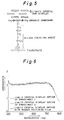
- An employed substrate is a glass substrate 1 with an ITO electrode 2 which is finely processed as shown in Fig. 1, and a material for an insulation film such as SiO 2 is rotationally applied to the substrate by using a spinner, followed by thermal treatment, in order to form an insulation film.
- a toluene solution (approximately 0.1 to 5%, preferably 1 to 3%) is prepared containing 1% silane coupling agent 10 of the structural formula (I) and the glass substrate 1 is dipped therein to conduct chemical adsorption of the silane coupling agent 10. After dipping, the substrate 1 is subjected to heat treatment at a temperature of 120°C (100 to 130°C) for about one hour and then the unreacted silane coupling agent is removed by washing the surface thereof with toluene.
- a glass container 7 shown in Fig. 2 holds a liquid crystal 6 for orientation control therein which is arranged in a certain direction and to which 1 wt% organic compound 12 of the structural formula (III) to be coupled with the silane coupling agent 10 in a certain direction was added.
- the addition amount of the organic compound to the liquid crystal is preferably 1 to 3 wt% which causes no crystallization.
- the mixture is homogeneously pre-melted at a temperature of 120°C.
- the reaction of the silane coupling agent upon the organic compound is caused by applying at least 8K gauss magnetic field, preferably 10 to 20K gauss to the mixture contained in the glass container 7 and heating up to approximately 100°C.
- the isotropic phase of liquid crystal molecules for orientation control makes it impossible to orient the organic compound 12, the molecules are necessary to be in a liquid crystal phase also at a temperature of approximately 100°C, and are further preferable to be in a nematic phase. Moreover, it is necessary that the organic compound 12 is homogeneously mixed with the liquid crystal 6 for orientation control without crystallization.
- a nematic liquid crystal of PDX-5080 transition temperature (°C) C-24 ⁇ N ⁇ 113 ⁇ 2 ⁇ I) manufactured by Rodic was used as a liquid crystal which meets the above-mentioned requirements.
- the glass substrate 1 is dipped in the mixture in the glass container 7 so that a surface of the glass substrate and a desired orientation direction of the liquid crystal are parallel with the direction of magnetic field application.
- the glass substrate 1 is taken out from the glass container 7 and the liquid crystal 6 for orientation control and the organic compound 12 unreacted with the silane coupling agent are removed by washing the glass substrate surface with toluene.
- a pair of substrates prepared in the above manner are joined to each other through a spacer 8 with a thickness of 12 ⁇ m excepting a one injection port to form a cell so that the orientation direction of the orientation film of each substrate is identical with that of each other as shown in Fig. 1, and the injection port is dipped in a nematic liquid crystal 5 of "E-8" manufactured by Merck in a vacuum state. By restoring to an atmospheric pressure, the liquid crystal is introduced into the cell to form a liquid crystal device.
- a further embodiment of the liquid crystal device in which a nematic liquid crystal was injected was produced and examined under the identical conditions with those of Embodiment 1 except that an employed mixture contained 3 wt% organic compound and the balance thereof was a nematic liquid crystal, "RDP-10848" (transition temperature (°C) C ⁇ -46 ⁇ N ⁇ 104 ⁇ 6 ⁇ 1).
- RDP-10848 transition temperature (°C) C ⁇ -46 ⁇ N ⁇ 104 ⁇ 6 ⁇ 1
- the structural formula of the employed organic compound which is coupled with the silane coupling agent is shown in formula (III). It was found that the liquid crystal orientation was uniformly homogeneous.
- a further embodiment of the liquid crystal device in which a nematic liquid crystal was injected was produced and examined under the identical conditions with those of Embodiment 1 except that an organic compound 13 shown in Structural Formula (IV) was employed as an organic compound which is coupled with the silane coupling agent in a certain direction.
- the liquid crystal orientation was uniformly homogenous.
- a further embodiment of the liquid crystal device in which a nematic liquid crystal was injected was produced and examined under the identical conditions with those of Embodiment 1 except the following points.
- An employed nematic liquid crystal was that under the designation "E-8" manufactured by Merck.
- An organic compound 14 shown in Structural Formula (V) was employed as an organic compound which is coupled with the silane coupling agent in a certain direction. The mixture of the liquid crystal and the organic compound was heated up to 60°C and kept for a one hour in this state.
- a further embodiment of the liquid crystal device in which a nematic liquid crystal was injected was produced and examined under the identical conditions with those of Embodiment 1 except that an organic compound 15 shown in Structural Formula (VI) was employed as an organic compound which is coupled with the silane coupling agent in a certain direction and the mixture of the organic compound and the liquid crystal for orientation was once premelted at a temperature of 140°C homogeneously. The orientation of the liquid crystal was found to be uniformly homogeneous.
- a further embodiment of the liquid crystal device in which a nematic liquid crystal was injected was produced and examined under the identical conditions with those of Embodiment 1 except that an organic compound 16 shown in Structural Formula (VII) was employed as an organic compound which is coupled with the silane coupling agent in a certain direction.
- the orientation of the liquid crystal was found to be uniformly homogeneous.
- a further embodiment of the liquid crystal device in which a nematic liquid crystal was injected was produced and examined under the identical conditions with those of Embodiment 1 except that a silane coupling agent 11 shown in Structural Formula (II) was employed as the silane coupling agent and an organic compound 16 shown in Structural Formula (VII) was employed as an organic compound which is coupled with the silane coupling agent in a certain direction.
- the orientation of the liquid crystal was found to be uniformly homogeneous.
- a glass substrate 1 on which a silane coupling agent was chemically adsorbed in Embodiment 1 and a glass substrate 3 with comb-shaped ITO electrodes 4 with a width of 10 ⁇ m and an interval of 500 ⁇ m therebetween were disposed to be opposite to each other through a spacer with a thickness of 12 ⁇ m and were fixed with a clip or the like, without sticking them together, to form a cell.
- an orientation controlling liquid crystal 6 which is the same as that of Embodiment 1 and an organic compound 12 with a symmetrical molecular structure about a longitudinal axis thereof was injected into the cell.
- the whole cell was heated up to approximately 100°C, applying a voltage of AC 100V 60Hz to he comb-shaped electrodes, and was kept for half an hour in this state.
- the cell was decomposed and the glass substrate 1 was washed with toluene, whereby an orientation film coated substrate was formed.
- a liquid crystal device was produced in the same manner as that of Embodiment 1 by using the glass substrate with an orientation film formed in the above manner. Additionally described, since an AC voltage is preferred to a DC voltage to uniformly orient, an AC voltage of 100V 60Hz is applied to the electrodes.
- non-uniformly oriented portions opposite to the comb-shaped electrodes might be applied for portions which are not used for displaying, when the substrate to which the orientation film is applied is practically employed.
- Still further embodiments of the liquid crystal device in which a nematic liquid crystal was injected were produced and examined under the identical conditions with those of Embodiment 8 except that conditions about employed materials and heating temperature are the same as those of Embodiments 2 to 7. It was found that, though the portions of the liquid crystal opposite to the comb-shaped electrodes were not oriented in a certain direction, the portions between the comb-shaped electrodes were oriented to be uniformly homogeneous.
Description


CH2=CHSi(OCH3)3

Claims (10)
- A method of forming an orientation film in situ with a liquid crystal comprising the following steps in the following order :(1) a silane coupling agent (10,11) is chemically adsorbed onto the surface of a substrate;(2) a liquid crystal compound (6) is mixed with an organic compound (12-16) which is miscible with, and orientable by, the liquid crystal compound (6) and has a functional group capable of chemically coupling with the coupling agent (10,11);(3) the mixture from step (2) is oriented in a magnetic or electrical field under conditions where the liquid crystal compound (6) is in a liquid crystal phase;(4) the substrate is brought into contact with the mixture and is aligned parallel to the orientation and the oriented organic compound (12) is caused to react with the coupling agent (10,11) to provide a substrate having a film of the organic compound (12) coupled to the coupling agent (10,11).
- A method according to claim 1, in which the product is washed free from uncoupled mixture.
- A method according to claim 1 or claim 2 in which the said organic compound (12-16) is coupled with the silane coupling agent (10,11) while an electrical field is applied in a chosen direction to the mixture containing the liquid crystal compound (6) at a temperature at which it is in a liquid crystal phase, and the substrate is dipped in the mixture so as to be directed toward a certain direction relative to a direction of the electrical field application and the mixture is heated till the silane coupling agent (10,11) and the organic compound (12-16) react with each other.
- A method according to claim 1 or claim 2 in which the said organic compound (12-16) is coupled with the silane coupling agent (10,11) in a certain direction by arranging a substrate (3) with a plurality of parallel stripe-shaped electrodes (4) formed on a surface thereof and the substrate on which said silane coupling agent (10,11) is chemically adsorbed so that they are disposed opposite to each other, said mixture being at a temperature at which the liquid crystal compound (6) is in a liquid crystal phase and disposed therebetween, and while a voltage is applied to the electrodes (4) so that polarities are different between the neighboring electrodes, the mixture is heated till the silane coupling agent (10,11) and the organic compound (12-16) react with each other.
- A method according to claim 1 or claim 2 in which the said organic compound (12-16) is coupled with the silane coupling agent (10,11) while a magnetic field is applied in a chosen direction to the mixture containing the liquid crystal compound (6) at a temperature at which it is in a liquid crystal phase, and the substrate is dipped in the mixture so as to be directed toward a certain direction relative to a direction of the magnetic field application and the mixture is heated till the silane coupling agent (10,11) and the organic compound (12-16) react with each other.
- A method as claimed in any one of claims 1 to 5, characterized in that the silane coupling agent has an epoxide group at one end and the organic compound has at least one hydroxyl or amino group.
- A method as claimed in any one of claims 1 to 5, characterized in that the silane coupling agent has a vinyl group and the organic compound has at least one amino group.
- A method as claimed in claim 6 or claim 7 in which the organic compound has more than one hydroxyl or amino group.
- A method as claimed in any one of claims 1 to 8, characterized in that the liquid crystal compound is in a nematic liquid crystal phase.
- A method for manufacturing a liquid crystal device characterized in that two substrates (1) with an orientation film (9) being formed according to a method as claimed in any one of claims 1 to 9 are disposed so that the orientation films (9) thereof face each other, the two substrates (1) are joined through a spacer to each other, and a gap between the substrate (1) being formed by the spacer is filled with a liquid crystal (5).
Applications Claiming Priority (2)
| Application Number | Priority Date | Filing Date | Title |
|---|---|---|---|
| JP331624/92 | 1992-12-11 | ||
| JP33162492 | 1992-12-11 |
Publications (2)
| Publication Number | Publication Date |
|---|---|
| EP0601895A1 EP0601895A1 (en) | 1994-06-15 |
| EP0601895B1 true EP0601895B1 (en) | 1998-05-06 |
Family
ID=18245740
Family Applications (1)
| Application Number | Title | Priority Date | Filing Date |
|---|---|---|---|
| EP93310040A Expired - Lifetime EP0601895B1 (en) | 1992-12-11 | 1993-12-13 | Method for forming an orientation film |
Country Status (4)
| Country | Link |
|---|---|
| US (1) | US5468519A (en) |
| EP (1) | EP0601895B1 (en) |
| DE (1) | DE69318380T2 (en) |
| TW (1) | TW293841B (en) |
Families Citing this family (14)
| Publication number | Priority date | Publication date | Assignee | Title |
|---|---|---|---|---|
| GB2293889A (en) * | 1994-10-03 | 1996-04-10 | Sharp Kk | Liquid crystal device and method of making a liquid crystal device |
| US5578351A (en) * | 1995-01-20 | 1996-11-26 | Geo-Centers, Inc. | Liquid crystal composition and alignment layer |
| US6275276B1 (en) * | 1995-10-06 | 2001-08-14 | Hitachi, Ltd. | Liquid crystal display with two liquid crystal gel layers each having a polymer enabling alignment |
| US6326640B1 (en) | 1996-01-29 | 2001-12-04 | Motorola, Inc. | Organic thin film transistor with enhanced carrier mobility |
| US5707691A (en) * | 1996-08-27 | 1998-01-13 | The Coca-Cola Company | Coating hollow containers by in-situ polymerization of monomers in bi-axially orientated form |
| US6517401B1 (en) | 1997-11-18 | 2003-02-11 | Matsushita Electric Industrial Co., Ltd. | Process for the production of monomolecular chemisorption film, and processes for the production of liquid crystal alignment films and liquid crystal displays by using the chemisorption film |
| US6545580B2 (en) | 1998-09-09 | 2003-04-08 | Veeco Instruments, Inc. | Electromagnetic field generator and method of operation |
| TW482932B (en) * | 1999-07-05 | 2002-04-11 | Matsushita Electric Ind Co Ltd | Chemical adsorbate compound, organic film, liquid crystal alignment film, and liquid crystal display device utilizing the chemical adsorbate compound |
| US6723396B1 (en) * | 1999-08-17 | 2004-04-20 | Western Washington University | Liquid crystal imprinting |
| US6734038B2 (en) * | 2001-09-04 | 2004-05-11 | The Trustees Of Princeton University | Method of manufacturing high-mobility organic thin films using organic vapor phase deposition |
| US20060121197A1 (en) * | 2003-09-05 | 2006-06-08 | Moffat William A | Method for silane coating of indium tin oxide surfaced substrates |
| US8121099B2 (en) | 2006-06-04 | 2012-02-21 | Asustek Computer Inc. | Voice over internet protocol system and related wireless local area network device |
| US8203139B2 (en) * | 2006-11-24 | 2012-06-19 | Idemitsu Kosan Co., Ltd | Organic thin film transistor and organic thin film light-emitting transistor using an organic semiconductor layer having an aromatic hydrocarbon group or an aromatic heterocyclic group in the center thereof |
| CN105481889B (en) * | 2015-11-17 | 2018-08-14 | 深圳市华星光电技术有限公司 | The production method of response type vertical orientation organosilicon material and liquid crystal display panel |
Family Cites Families (13)
| Publication number | Priority date | Publication date | Assignee | Title |
|---|---|---|---|---|
| JPS5779915A (en) * | 1980-11-07 | 1982-05-19 | Hitachi Ltd | Formation of liquid crystal orientation film |
| JPS58123519A (en) * | 1982-01-19 | 1983-07-22 | Sharp Corp | Liquid crystal display |
| JPS58123520A (en) * | 1982-01-19 | 1983-07-22 | Sharp Corp | Liquid crystal display |
| JPH0750284B2 (en) * | 1985-12-27 | 1995-05-31 | 株式会社日立製作所 | Optical path switch |
| JPS62245218A (en) * | 1986-04-18 | 1987-10-26 | Seiko Epson Corp | Production of liquid crystal display device |
| EP0261712A1 (en) * | 1986-09-04 | 1988-03-30 | Koninklijke Philips Electronics N.V. | Picture display cell, method of forming an orientation layer on a substrate of the picture display cell and monomeric compounds for use in the orientation layer |
| DE3881726T2 (en) * | 1987-03-09 | 1994-01-13 | Chisso Corp | Diamino compounds and films for the orientation of liquid crystals. |
| JPS646924A (en) * | 1987-06-29 | 1989-01-11 | Matsushita Electric Ind Co Ltd | Electric field effect type liquid crystal display element |
| JPH02165119A (en) * | 1988-12-20 | 1990-06-26 | Matsushita Electric Ind Co Ltd | Production of oriented film for liquid crystal |
| US5133895A (en) * | 1989-03-09 | 1992-07-28 | Matsushita Electric Industrial Co., Ltd. | Alignment film for liquid crystal and method for production thereof, as well as liquid crystal display device utilizing said alignment film and method for production thereof |
| US5256456A (en) * | 1990-09-17 | 1993-10-26 | Matsushita Electric Industrial Co., Ltd. | Liquid crystal alignment film and method of manufacturing the same |
| JPH04204416A (en) * | 1990-11-29 | 1992-07-24 | Matsushita Electric Ind Co Ltd | Production of liquid crystal element |
| US5315419A (en) * | 1992-05-19 | 1994-05-24 | Kent State University | Method of producing a homogeneously aligned chiral smectic C liquid crystal having homeotropic alignment layers |
-
1993
- 1993-12-03 TW TW082110220A patent/TW293841B/zh active
- 1993-12-08 US US08/163,863 patent/US5468519A/en not_active Expired - Fee Related
- 1993-12-13 EP EP93310040A patent/EP0601895B1/en not_active Expired - Lifetime
- 1993-12-13 DE DE69318380T patent/DE69318380T2/en not_active Expired - Fee Related
Also Published As
| Publication number | Publication date |
|---|---|
| TW293841B (en) | 1996-12-21 |
| US5468519A (en) | 1995-11-21 |
| DE69318380D1 (en) | 1998-06-10 |
| EP0601895A1 (en) | 1994-06-15 |
| DE69318380T2 (en) | 1998-11-19 |
Similar Documents
| Publication | Publication Date | Title |
|---|---|---|
| EP0601895B1 (en) | Method for forming an orientation film | |
| EP0386782B1 (en) | Alignment film for liquid crystal and method for production thereof, as well as liquid crystal display device utilizing said alignment film and method for production thereof | |
| KR19980701504A (en) | Liquid crystal composition and alignment layer | |
| JP2567404B2 (en) | Liquid crystal device and its manufacturing method | |
| JP2698717B2 (en) | Liquid crystal alignment film, method of manufacturing the same, liquid crystal display device and method of manufacturing the same | |
| JPS62174725A (en) | Liquid crystal display device | |
| EP0365855A1 (en) | Orientation layer composition for liquid crystal display devices | |
| EP0571681A1 (en) | A method of forming a film for use in alignment of liquid crystal | |
| JP2558903B2 (en) | Liquid crystal alignment film, manufacturing method thereof, and liquid crystal display device using the same | |
| JP2955457B2 (en) | Method of forming alignment film | |
| Ohtake et al. | A liquid crystal display having a rubbing-free photo-aligned monomolecular layer as an alignment film | |
| TW548490B (en) | Improvements in liquid crystal displays | |
| JP3083477B2 (en) | Liquid crystal alignment film, method of manufacturing the same, and liquid crystal display device using the same | |
| JPH04141625A (en) | Liquid crystal element | |
| JP3161645B2 (en) | Liquid crystal alignment film, method of manufacturing the same, and liquid crystal display device | |
| JPH09218411A (en) | Liquid crystal display element | |
| JPH04240620A (en) | Liquid crystal oriented film | |
| KR0183375B1 (en) | Liquid crystal device with chemically-induced high-tilt alignment coating | |
| JPS63253921A (en) | Liquid crystal element | |
| JP2541806B2 (en) | Method for forming alignment film for liquid crystal display device | |
| JPH02287432A (en) | Oriented film for liquid crystal and twisted nematic liquid crystal cell | |
| JPH0359622A (en) | Liquid crystal display element | |
| JPH01172927A (en) | Liquid crystal element | |
| JPH05150242A (en) | Liquid crystal element | |
| JPH0611717A (en) | Liquid crystal element |
Legal Events
| Date | Code | Title | Description |
|---|---|---|---|
| PUAI | Public reference made under article 153(3) epc to a published international application that has entered the european phase |
Free format text: ORIGINAL CODE: 0009012 |
|
| AK | Designated contracting states |
Kind code of ref document: A1 Designated state(s): DE GB |
|
| 17P | Request for examination filed |
Effective date: 19940916 |
|
| 17Q | First examination report despatched |
Effective date: 19960703 |
|
| GRAG | Despatch of communication of intention to grant |
Free format text: ORIGINAL CODE: EPIDOS AGRA |
|
| GRAG | Despatch of communication of intention to grant |
Free format text: ORIGINAL CODE: EPIDOS AGRA |
|
| GRAH | Despatch of communication of intention to grant a patent |
Free format text: ORIGINAL CODE: EPIDOS IGRA |
|
| GRAH | Despatch of communication of intention to grant a patent |
Free format text: ORIGINAL CODE: EPIDOS IGRA |
|
| GRAA | (expected) grant |
Free format text: ORIGINAL CODE: 0009210 |
|
| AK | Designated contracting states |
Kind code of ref document: B1 Designated state(s): DE GB |
|
| REF | Corresponds to: |
Ref document number: 69318380 Country of ref document: DE Date of ref document: 19980610 |
|
| PLBE | No opposition filed within time limit |
Free format text: ORIGINAL CODE: 0009261 |
|
| STAA | Information on the status of an ep patent application or granted ep patent |
Free format text: STATUS: NO OPPOSITION FILED WITHIN TIME LIMIT |
|
| 26N | No opposition filed | ||
| REG | Reference to a national code |
Ref country code: GB Ref legal event code: IF02 |
|
| PGFP | Annual fee paid to national office [announced via postgrant information from national office to epo] |
Ref country code: GB Payment date: 20021211 Year of fee payment: 10 |
|
| PGFP | Annual fee paid to national office [announced via postgrant information from national office to epo] |
Ref country code: DE Payment date: 20021219 Year of fee payment: 10 |
|
| PG25 | Lapsed in a contracting state [announced via postgrant information from national office to epo] |
Ref country code: GB Free format text: LAPSE BECAUSE OF NON-PAYMENT OF DUE FEES Effective date: 20031213 |
|
| PG25 | Lapsed in a contracting state [announced via postgrant information from national office to epo] |
Ref country code: DE Free format text: LAPSE BECAUSE OF NON-PAYMENT OF DUE FEES Effective date: 20040701 |
|
| GBPC | Gb: european patent ceased through non-payment of renewal fee |
Effective date: 20031213 |