EP0601740B1 - HF-Verstärker mit linearer Verstärkungssteuerung - Google Patents
HF-Verstärker mit linearer Verstärkungssteuerung Download PDFInfo
- Publication number
- EP0601740B1 EP0601740B1 EP93309402A EP93309402A EP0601740B1 EP 0601740 B1 EP0601740 B1 EP 0601740B1 EP 93309402 A EP93309402 A EP 93309402A EP 93309402 A EP93309402 A EP 93309402A EP 0601740 B1 EP0601740 B1 EP 0601740B1
- Authority
- EP
- European Patent Office
- Prior art keywords
- admittance
- circuit
- pin diode
- node
- transistor
- Prior art date
- Legal status (The legal status is an assumption and is not a legal conclusion. Google has not performed a legal analysis and makes no representation as to the accuracy of the status listed.)
- Expired - Lifetime
Links
Images

Classifications
-
- H—ELECTRICITY
- H03—ELECTRONIC CIRCUITRY
- H03G—CONTROL OF AMPLIFICATION
- H03G3/00—Gain control in amplifiers or frequency changers
- H03G3/20—Automatic control
- H03G3/30—Automatic control in amplifiers having semiconductor devices
- H03G3/3036—Automatic control in amplifiers having semiconductor devices in high-frequency amplifiers or in frequency-changers
- H03G3/3042—Automatic control in amplifiers having semiconductor devices in high-frequency amplifiers or in frequency-changers in modulators, frequency-changers, transmitters or power amplifiers
-
- H—ELECTRICITY
- H03—ELECTRONIC CIRCUITRY
- H03G—CONTROL OF AMPLIFICATION
- H03G7/00—Volume compression or expansion in amplifiers
- H03G7/001—Volume compression or expansion in amplifiers without controlling loop
Definitions
- a circuit for amplifying an input radio frequency band of signals wherein signal gain in decibels is a linear function of the logarithm of a control signal, said circuit comprising: a first transistor amplifier stage having an output node exhibiting a first RF complex admittance within said frequency band of signals; a second transistor amplifier stage having an input node exhibiting a second RF complex admittance within said frequency band of signals.
Landscapes
- Amplifiers (AREA)
- Control Of Amplification And Gain Control (AREA)
Claims (8)
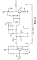
- Schaltung zum Verstärken eines eingegebenen Hochfrequenz(HF)-Signalbands, wobei die Signalverstärkung in Dezibel (dB) eine lineare Funktion des Logarithmus eines Steuerungssignals ist, mit:dadurch gekennzeichnet, dasseiner ersten Transistorverstärkerstufe (10, 20, 22, 24, 26; 50, 62) mit einem Ausgangsknoten (KNOTEN 1; KNOTEN_1), der einen ersten komplexen HF-Scheinleitwert innerhalb des Signalfrequenzbands zeigt;einer zweiten Transistorverstärkerstufe (12, 30, 32, 34; 52, Rc) mit einem Eingangsknoten, der innerhalb des Signalfrequenzbands einen zweiten komplexen HF-Scheinleitwert zeigt und mit dem Ausgangsknoten der ersten Verstärkerstufe verbunden ist;die zweite Transistorverstärkerstufe (12, 30, 32, 34; 52, Rc) eine Steuerelektrode, eine zweite, mit einer Spannungsversorgung verbundene Elektrode sowie eine dritte, über einen Widerstand (34; Rc) mit einem gemeinsamen Potential verbundene Elektrode aufweist, wobei der Widerstand den zweiten komplexen HF-Scheinleitwert beeinflusst und die Steuerelektrode mit dem Ausgangsknoten (KNOTEN 1; KNOTEN_1) verbunden ist;eine pin-Diodeneinrichtung (40; 58) vorhanden ist, die zwischen einen Steuerungssignaleingang (42; 60) und den Ausgangsknoten (KNOTEN 1, KNOTEN_1) geschaltet ist und auf ein Steuerungssignal anspricht, um einen vorgegebenen HF-Scheinleitwert wiederzuspiegeln, wobei diese pin-Diodeneinrichtung ferner über einen HF-Pfad (44) mit dem gemeinsamen Potential verbunden ist; undeine HF-Reaktanzeinrichtung (36, 38; 54, 56) im Nebenschluss in Bezug auf den HF-Pfad der pin-Diodeneinrichtung (40; 58) zwischen das gemeinsame Potential und den Ausgangsknoten geschaltet ist und sie einen dritten komplexen HF-Scheinleitwert aufweist, der höher als der erste und der zweite komplexe Scheinleitwert gewählt ist und imaginäre Anteile des ersten und des zweiten komplexen Scheinleitwerts aufhebt, wodurch jeder durch die pin-Diodeneinrichtung gesehene Scheinleitwert innerhalb des Signalfrequenzbands im Wesentlichen reell ist.
- Schaltung nach Anspruch 1, dadurch gekennzeichnet, dass Variationen im eingegebenen Steuerungssignal so wirken, dass sie den HF-Widerstand der pin-Diodeneinrichtung (40) variieren, um dadurch Anteile des hochfrequenten Signalbands zum gemeinsamen Potential nebenzuschließen, wobei die Variation zu einer linearen Verstärkungsänderung führt.
- Schaltung nach Anspruch 2, dadurch gekennzeichnet, dass die HF-Einrichtung (36, 38; 54, 56) ein Induktivität/Kondensator-Paar in Parallelschaltung aufweist.
- Schaltung nach Anspruch 3, dadurch gekennzeichnet, dass der vorgegebene HF-Scheinleitwert der pin-Diodeneinrichtung viel größer als der erste oder zweite komplexe HF-Scheinleitwert ist.
- Schaltung nach Anspruch 1, dadurch gekennzeichnet, dass die erste und die zweite Verstärkerstufe MOSFET-Transistoren enthalten, wobei ein Anschluss eines MOSFET-Transistors in der ersten Verstärkerstufe in HF-Verbindung mit dem Gate eines MOSFET-Transistors in der zweiten Verstärkerstufe steht, wobei beide MOSFETs reelle Anteile der Scheinleitwerte zeigen, die klein in Bezug auf den reellen Anteil des Scheinleitwerts sind, den die pin-Diodeneinrichtung zeigt.
- Schaltung nach Anspruch 1, dadurch gekennzeichnet, dass die erste und die zweite Verstärkerstufe bipolare Transistoren enthalten, wobei der Kollektor eines bipolaren Transistors in der ersten Verstärkerstufe in HF-Verbindung mit der Basis eines bipolaren Transistors in der zweiten Verstärkerstufe steht und wobei diese bipolaren Transistoren eine kleine Rückkopplungskapazität von der Basis auf den Kollektor zeigen.
- Schaltung nach Anspruch 6, dadurch gekennzeichnet, dass der Emitter des bipolaren Transistors in der zweiten Verstärkerstufe über den Widerstand mit dem gemeinsamen Potential verbunden ist, wobei der Wert des Widerstands, in Kombination mit dem Betawert des zweiten Transistors, so wirkt, dass er an der Basis des bipolaren Transistors in der zweiten Verstärkerschaltung einen niedrigen Eingangs-Scheinleitwert erzeugt.
- Schaltung nach Anspruch 2, ferner mit einem Widerstand, der die pin-Diodeneinrichtung mit dem gemeinsamen Potential verbindet und für einen Konstantstrompfad für einen ersten Teil des Steuerungssignals sorgt, wobei das eingegebene Steuerungssignal ein Gleichstrom ist, und mit einem zweiten Teil, der variabel ist, so dass dann, wenn der variable Teil klein ist und in ihm Änderungen auftreten, die pin-Diodeneinrichtung durch kombinierte Effekte des ersten Teils und des zweiten Teils des Steuerungssignals eine Änderung des Scheinleitwerts erfährt, die Nichtlinearitäten in der Verstärkungssteuerung, die aus irgendeinem Scheinleitwert herrühren, wie er von der pin-Diodeneinrichtung gesehen wird, einem Versatz unterzieht.
Applications Claiming Priority (2)
| Application Number | Priority Date | Filing Date | Title |
|---|---|---|---|
| US989116 | 1992-12-11 | ||
| US07/989,116 US5304948A (en) | 1992-12-11 | 1992-12-11 | RF amplifier with linear gain control |
Publications (3)
| Publication Number | Publication Date |
|---|---|
| EP0601740A2 EP0601740A2 (de) | 1994-06-15 |
| EP0601740A3 EP0601740A3 (de) | 1995-06-14 |
| EP0601740B1 true EP0601740B1 (de) | 1999-03-31 |
Family
ID=25534779
Family Applications (1)
| Application Number | Title | Priority Date | Filing Date |
|---|---|---|---|
| EP93309402A Expired - Lifetime EP0601740B1 (de) | 1992-12-11 | 1993-11-25 | HF-Verstärker mit linearer Verstärkungssteuerung |
Country Status (3)
| Country | Link |
|---|---|
| US (1) | US5304948A (de) |
| EP (1) | EP0601740B1 (de) |
| DE (1) | DE69324215T2 (de) |
Families Citing this family (8)
| Publication number | Priority date | Publication date | Assignee | Title |
|---|---|---|---|---|
| DE69624673T2 (de) * | 1996-01-17 | 2003-09-18 | Nokia Corp., Espoo | Verfahren zur Ausdehnung des Bereichs eines Empfangssignalstärkenindikators und nach diesem Verfahren arbeitender Funksendeempfänger |
| GB2318004A (en) * | 1996-10-01 | 1998-04-08 | Nokia Mobile Phones Ltd | A diode detector |
| US6271727B1 (en) | 1999-08-06 | 2001-08-07 | Rf Micro Devices, Inc. | High isolation RF power amplifier with self-bias attenuator |
| US7545774B1 (en) | 1999-08-26 | 2009-06-09 | Nokia Corporation | Method for indicating power consumption in a packet switched communication system |
| US6414547B1 (en) | 2000-09-29 | 2002-07-02 | International Business Machines Corporation | Variable gain RF amplifier |
| US6586833B2 (en) | 2000-11-16 | 2003-07-01 | Silicon Semiconductor Corporation | Packaged power devices having vertical power mosfets therein that are flip-chip mounted to slotted gate electrode strip lines |
| US6906592B2 (en) | 2002-11-13 | 2005-06-14 | Qualcomm Inc | Continuously variable gain radio frequency driver amplifier having linear in decibel gain control characteristics |
| JP4559772B2 (ja) * | 2004-05-31 | 2010-10-13 | パナソニック株式会社 | スイッチ回路 |
Family Cites Families (3)
| Publication number | Priority date | Publication date | Assignee | Title |
|---|---|---|---|---|
| DE1537690C3 (de) * | 1967-09-20 | 1975-02-13 | Siemens Ag, 1000 Berlin Und 8000 Muenchen | Transistorbestückter Breitbandverstärker mit einer Verstärkungsregelung |
| US3534278A (en) * | 1969-03-03 | 1970-10-13 | Bell Telephone Labor Inc | Variolossers having substantially flat frequency response characteristics at all loss settings |
| US4677392A (en) * | 1985-12-16 | 1987-06-30 | Hughes Aircraft Company | Cascaded internal impedance dependent amplifier with accurate variable gain control |
-
1992
- 1992-12-11 US US07/989,116 patent/US5304948A/en not_active Expired - Lifetime
-
1993
- 1993-11-25 DE DE69324215T patent/DE69324215T2/de not_active Expired - Fee Related
- 1993-11-25 EP EP93309402A patent/EP0601740B1/de not_active Expired - Lifetime
Also Published As
| Publication number | Publication date |
|---|---|
| EP0601740A2 (de) | 1994-06-15 |
| DE69324215D1 (de) | 1999-05-06 |
| US5304948A (en) | 1994-04-19 |
| DE69324215T2 (de) | 1999-09-30 |
| EP0601740A3 (de) | 1995-06-14 |
Similar Documents
| Publication | Publication Date | Title |
|---|---|---|
| KR100480071B1 (ko) | 가변 감쇠기 | |
| AU648364B2 (en) | Linear gain control amplifier | |
| US4788511A (en) | Distributed power amplifier | |
| KR100772743B1 (ko) | 무선 주파수 디바이스 및 이를 구비한 무선 주파수 수신기및 캐패시턴스 충전 방법 | |
| EP0886384A2 (de) | Rauscharmer Zweibandverstärker mit einem einzigen Stufe für einen drahtlosen Funkkommunikationsempfänger | |
| US5307026A (en) | Variable gain RF amplifier with linear gain control | |
| US4367443A (en) | Radio frequency signal power amplifier | |
| US4967169A (en) | FET monolithic microwave integrated circuit variable slope gain-equalizer | |
| US7999608B1 (en) | Integrated RF notch filters | |
| US20230006623A1 (en) | Bias circuit of power amplifier, device and equipment | |
| US6426677B1 (en) | Linearization bias circuit for BJT amplifiers | |
| US5694085A (en) | High-power amplifier using parallel transistors | |
| US5339048A (en) | Radio frequency amplifier | |
| EP0601740B1 (de) | HF-Verstärker mit linearer Verstärkungssteuerung | |
| Walker | A low phase shift attenuator | |
| US5424686A (en) | Negative-resistance-compensated microwave buffer | |
| EP0250453B1 (de) | Genaue verstärkungsregelung eines kettenverstärkers mit regelbarer innenimpedanz | |
| US7242253B2 (en) | Low noise amplifier | |
| KR910000694B1 (ko) | 고주파증폭장치 | |
| US6400222B1 (en) | Linearizer | |
| US3534278A (en) | Variolossers having substantially flat frequency response characteristics at all loss settings | |
| USRE29844E (en) | Unit transistor amplifier with matched input and output impedances | |
| KR200308685Y1 (ko) | 저잡음증폭기 | |
| US5446415A (en) | Intermediate frequency amplifier circuit | |
| US20020000888A1 (en) | Low phase noise variable frequency oscillator |
Legal Events
| Date | Code | Title | Description |
|---|---|---|---|
| PUAI | Public reference made under article 153(3) epc to a published international application that has entered the european phase |
Free format text: ORIGINAL CODE: 0009012 |
|
| AK | Designated contracting states |
Kind code of ref document: A2 Designated state(s): DE FR GB SE |
|
| RIN1 | Information on inventor provided before grant (corrected) |
Inventor name: MUCKE, LARS HENRIK |
|
| PUAL | Search report despatched |
Free format text: ORIGINAL CODE: 0009013 |
|
| AK | Designated contracting states |
Kind code of ref document: A3 Designated state(s): DE FR GB SE |
|
| 17P | Request for examination filed |
Effective date: 19951214 |
|
| 17Q | First examination report despatched |
Effective date: 19971105 |
|
| RAP1 | Party data changed (applicant data changed or rights of an application transferred) |
Owner name: NOKIA MOBILE PHONES LTD. |
|
| GRAG | Despatch of communication of intention to grant |
Free format text: ORIGINAL CODE: EPIDOS AGRA |
|
| GRAG | Despatch of communication of intention to grant |
Free format text: ORIGINAL CODE: EPIDOS AGRA |
|
| GRAH | Despatch of communication of intention to grant a patent |
Free format text: ORIGINAL CODE: EPIDOS IGRA |
|
| GRAH | Despatch of communication of intention to grant a patent |
Free format text: ORIGINAL CODE: EPIDOS IGRA |
|
| GRAA | (expected) grant |
Free format text: ORIGINAL CODE: 0009210 |
|
| AK | Designated contracting states |
Kind code of ref document: B1 Designated state(s): DE FR GB SE |
|
| REF | Corresponds to: |
Ref document number: 69324215 Country of ref document: DE Date of ref document: 19990506 |
|
| ET | Fr: translation filed | ||
| PLBE | No opposition filed within time limit |
Free format text: ORIGINAL CODE: 0009261 |
|
| 26N | No opposition filed | ||
| REG | Reference to a national code |
Ref country code: GB Ref legal event code: IF02 |
|
| REG | Reference to a national code |
Ref country code: GB Ref legal event code: 732E |
|
| PGFP | Annual fee paid to national office [announced via postgrant information from national office to epo] |
Ref country code: SE Payment date: 20031105 Year of fee payment: 11 |
|
| PGFP | Annual fee paid to national office [announced via postgrant information from national office to epo] |
Ref country code: FR Payment date: 20031110 Year of fee payment: 11 |
|
| PGFP | Annual fee paid to national office [announced via postgrant information from national office to epo] |
Ref country code: GB Payment date: 20031119 Year of fee payment: 11 |
|
| PGFP | Annual fee paid to national office [announced via postgrant information from national office to epo] |
Ref country code: DE Payment date: 20031204 Year of fee payment: 11 |
|
| PG25 | Lapsed in a contracting state [announced via postgrant information from national office to epo] |
Ref country code: GB Free format text: LAPSE BECAUSE OF NON-PAYMENT OF DUE FEES Effective date: 20041125 |
|
| PG25 | Lapsed in a contracting state [announced via postgrant information from national office to epo] |
Ref country code: SE Free format text: LAPSE BECAUSE OF NON-PAYMENT OF DUE FEES Effective date: 20041126 |
|
| PG25 | Lapsed in a contracting state [announced via postgrant information from national office to epo] |
Ref country code: DE Free format text: LAPSE BECAUSE OF NON-PAYMENT OF DUE FEES Effective date: 20050601 |
|
| EUG | Se: european patent has lapsed | ||
| GBPC | Gb: european patent ceased through non-payment of renewal fee |
Effective date: 20041125 |
|
| PG25 | Lapsed in a contracting state [announced via postgrant information from national office to epo] |
Ref country code: FR Free format text: LAPSE BECAUSE OF NON-PAYMENT OF DUE FEES Effective date: 20050729 |
|
| REG | Reference to a national code |
Ref country code: FR Ref legal event code: ST |