EP0601072B1 - Elektrophoretische anzeigevorrichtung mit verschachtelter lokaler anode - Google Patents
Elektrophoretische anzeigevorrichtung mit verschachtelter lokaler anode Download PDFInfo
- Publication number
- EP0601072B1 EP0601072B1 EP92919073A EP92919073A EP0601072B1 EP 0601072 B1 EP0601072 B1 EP 0601072B1 EP 92919073 A EP92919073 A EP 92919073A EP 92919073 A EP92919073 A EP 92919073A EP 0601072 B1 EP0601072 B1 EP 0601072B1
- Authority
- EP
- European Patent Office
- Prior art keywords
- elements
- display
- lines
- grid
- anode
- Prior art date
- Legal status (The legal status is an assumption and is not a legal conclusion. Google has not performed a legal analysis and makes no representation as to the accuracy of the status listed.)
- Expired - Lifetime
Links
Images


Classifications
-
- G—PHYSICS
- G02—OPTICS
- G02F—OPTICAL DEVICES OR ARRANGEMENTS FOR THE CONTROL OF LIGHT BY MODIFICATION OF THE OPTICAL PROPERTIES OF THE MEDIA OF THE ELEMENTS INVOLVED THEREIN; NON-LINEAR OPTICS; FREQUENCY-CHANGING OF LIGHT; OPTICAL LOGIC ELEMENTS; OPTICAL ANALOGUE/DIGITAL CONVERTERS
- G02F1/00—Devices or arrangements for the control of the intensity, colour, phase, polarisation or direction of light arriving from an independent light source, e.g. switching, gating or modulating; Non-linear optics
- G02F1/01—Devices or arrangements for the control of the intensity, colour, phase, polarisation or direction of light arriving from an independent light source, e.g. switching, gating or modulating; Non-linear optics for the control of the intensity, phase, polarisation or colour
- G02F1/165—Devices or arrangements for the control of the intensity, colour, phase, polarisation or direction of light arriving from an independent light source, e.g. switching, gating or modulating; Non-linear optics for the control of the intensity, phase, polarisation or colour based on translational movement of particles in a fluid under the influence of an applied field
- G02F1/166—Devices or arrangements for the control of the intensity, colour, phase, polarisation or direction of light arriving from an independent light source, e.g. switching, gating or modulating; Non-linear optics for the control of the intensity, phase, polarisation or colour based on translational movement of particles in a fluid under the influence of an applied field characterised by the electro-optical or magneto-optical effect
- G02F1/167—Devices or arrangements for the control of the intensity, colour, phase, polarisation or direction of light arriving from an independent light source, e.g. switching, gating or modulating; Non-linear optics for the control of the intensity, phase, polarisation or colour based on translational movement of particles in a fluid under the influence of an applied field characterised by the electro-optical or magneto-optical effect by electrophoresis
Definitions
- the present invention relates to an electrophoretic display panel apparatus and methods for making same and, more particularly, to electrophoretic display panels with a local anode having elements which are interleaved with the grid elements of the display for assisting in the control of pigment particle migration and position.
- Electrophoretic displays are now well known. A variety of display types and features are taught in several patents issued in the names of the inventors herein, Frank J. DiSanto and Denis A. Krusos and assigned to the assignee herein, Copytele, Inc. of Huntington Station, New York.
- U.S Patent Nos. 4,655,897 and 4,732,830 each entitled ELECTROPHORETIC DISPLAY PANELS AND ASSOCIATED METHODS describe the basic operation and construction of an electrophoretic display.
- U.S. Patent No. 4,742,345, entitled ELECTROPHORETIC DISPLAY PANELS AND METHODS THEREFOR describes a display having improved alignment and contrast.
- the display panels shown in the above-mentioned patents operate upon the same basic principle, viz., if a suspension of electrically charged pigment particles in a dielectric fluid is subjected to an applied electrostatic field, the pigment particles will migrate through the fluid in response to the electrostatic field. Given a substantially homogeneous suspension of particles having a pigment color different from that of the dielectric fluid, if the applied electrostatic field is localized it will cause a visually observable localized pigment particle migration. The localized pigment particle migration results either in a localized area of concentration or rarefaction of particles depending upon the sign and direction of the electrostatic field and the charge on the pigment particles.
- Patents are "triode-type" displays having a plurality of independent, parallel, cathode row conductor elements or "lines” deposited in the horizontal on one surface of a glass viewing screen.
- a glass cap member forms a fluid-tight seal with the viewing window along the cap's peripheral edge for containing the fluid suspension and also acts as a substrate for an anode plate deposited on the interior flat surface of the cap.
- the anode surface is in spaced parallel relation to both the cathode elements and the grid elements.
- the cathode element voltage, the anode voltage, and the grid element voltage can then be ascertained such that when a particular voltage is applied to the cathode and another voltage is applied to the grid, the area proximate their intersection will assume a net charge sufficient to attract or repel pigment particles in suspension in the dielectric fluid. Since numerous cathode and grid lines are employed, there are numerous discrete intersection points which can be controlled by varying the voltage on the cathode and grid elements to cause localized visible regions of pigment concentration and rarefaction.
- the operating voltages on both cathode and grid must be able to assume at least two states corresponding to a logical one and a logical zero.
- Logical one for the cathode may either correspond to attraction or repulsion of pigment.
- the cathode and grid voltages are selected such that only when both are a logical one at a particular intersection point, will a sufficient electrostatic field be present at the intersection relative to the anode to cause the writing of a visual bit of information on the display through migration of pigment particles.
- the bit may be erased, e.g., upon a reversal of polarity and a logical zero-zero state occurring at the intersection coordinated with an erase voltage gradient between anode and cathode. In this manner, digitized data can be displayed on the electrophoretic display.
- EPID construction is described in Application No. 07/345,825, referred to above, which relates to an electrophoretic display in which the cathode/grid matrix as is found in triode-type displays is overlayed by a plurality of independent separately addressable "local" anode lines.
- the local anode lines are deposited upon and align with the grid lines and are insulated therefrom by interstitial lines of photoresist.
- the local anode lines are in addition to the "remote" anode, which is the layer deposited upon the anode faceplate or cap as in triode displays.
- the dual anode structure aforesaid provides enhanced operation by eliminating unwanted variations in display brightness between frames, increasing the speed of the display and decreasing the anode voltage required during Write and Hold cycles, all as explained in Application No. 07/345,825.
- the problems and disadvantages associated with conventional electrophoretic displays are overcome by the present invention which consists of an electrophoretic display as defined in claims 1 and 10 and a method for fabricating an electrode matrix for such displays as defined in claim 17.
- the inventive electrophoretic displays have : a cathode matrix comprising a plurality of parallel lines arranged in a given direction, a grid matrix insulated from the cathode matrix and comprising a plurality of parallel lines each perpendicular to the cathode lines to form an X-Y addressing matrix, and a conventional anode electrode separated from the X-Y matrix, the space between the anode electrode and the X-Y matrix accommodating an electrophoretic dispersion including pigment particles suspended in a fluid; the improvement therewith of an additional anode electrode comprising a plurality of parallel lines each associated with and insulated from the grid lines.
- the additional anode electrode is disposed within a plane shared by the grid matrix and operates to control the path of the pigment particles to and from the X-Y matrix and to
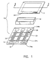
- FIG. 1 is an exploded perspective view of an electrophoretic display in accordance with an exemplary embodiment of the present invention.
- FIG. 2 is an enlarged plan view of a selected local anode element interleaved with a selected grid element in accordance with an exemplary embodiment of the present invention and as shown in FIG. 1.
- FIG.3 is a cross-sectional view of the electrophoretic display shown in FIG. 1 in the unexploded state, taken along section line III-III and looking in the direction of the arrows.
- FIG. 4 is an enlarged plan view of a selected grid and/or local anode element structure as is taught in prior Application No. 07/345,825 filed by the inventors herein.
- FIG.5 is a cross-sectional fragmentary view of an electrophoretic display in accordance with Application No. 07/345,825 and which incorporates the element structure shown in FIG. 4.
- FIG. 1 shows an electrophoretic display 10 in accordance with the present invention.
- the display 10 has an anode faceplate 12 and a cathode faceplate 14 which are sealably affixed on either side of an interstitial spacer 16 to form a fluid-tight envelope for containing a dielectric/pigment particle suspension or electrophoretic fluid (not shown).
- the faceplates 12 and 14 are typically flat glass plates upon which are deposited conductor elements to comprise the situs of electrostatic charge for inducing motion in the electrophoretic fluid.
- the techniques, materials and dimensions used to form the conductor elements upon the faceplates and the methods for making EPIDS, in general, are shown in U.S. Patent Nos. 4,655,897, 4,732,830 and 4,742,345.
- a plurality of independent, electrically conductive cathode lines 18, shown here as horizontal rows, are deposited upon the cathode faceplate 14 using conventional deposition and etching techniques.
- the orientation of the cathode lines depends upon the orientation of the screen, which, if rotated 90 degrees, would position the cathode lines vertically, thus, the cathode lines are arbitrarily defined as horizontal.
- the cathode elements 18 be composed of Indium Tin Oxide (ITO) as set forth in U.S. Patent No. 4,742,345.
- a plurality of independent grid conductor lines 20 are superposed in the vertical over the cathode elements 18, i.e., at right angles thereto, and are insulated therefrom by an interstitial photoresist layer 22 (see FIG. 2).
- the grid elements 20 may be formed by coating the photoresist layer 22 with a metal, such as nickel, using sputtering techniques or the like, and then selectively masking and etching to yield the intersecting but insulated configuration shown in FIG. 1.
- Each cathode and grid element 18, 20 terminates at one end in a contact pad 24c and 24g, respectively, or is otherwise adapted to permit connection to display driver circuitry (not shown).
- An anode 26 is formed on an interior surface of the anode faceplate 12 by plating with a thin layer of conductor material, such as, chrome.
- the present invention includes a novel local anode 28 structure.
- the benefits and operation of an EPID having a local anode have been recognized and described in Application No. 07/345,825 by the present Applicants.
- the local anode lines have been formed superposed over and in alignment with the grid elements, and separated therefrom by an interstitial layer of photoresist insulation (see FIG. 5).
- the local anode 28 lines are formed at the same time, of the same material and in the same plane as the grid elements 20. This is accomplished by interleaving the local anode 28 and grid 20 elements.
- the mask that was used to form the plurality of grid lines has been altered such that a plurality of grid lines and a plurality of local anode lines are simultaneously formed by a single mask.
- a SiO 2 coating can be applied over the grid/local anode/cathode complex as set forth in Application No. 07/345,825.
- the display is also operated in the same fashion as in that application.
- FIG. 2 shows an exemplary configuration for a single grid line 20, a single local anode line 28 and their interleaving.
- the configuration of the grid lines as a tined element i.e., a element having a plurality of coextensive parallel forks 30 emanating from a common area, here the grid contact pad 24g, improves display brightness as described in U.S. Patent No. 4,742,345.
- the local anode 28 is depicted as having a single elongated portion 32 emanating from a contact pad portion 241a.
- the elongated portion 32 of the local anode 28 extends between the forks 30 of the grid line 20, and, in this sense, interleaves with the grid line 20.
- the local anode 28 could also be provided with forks like those of the grid line 20, and in that event, the interleaving could be in the form of alternating grid and local anode forks. Indeed, any number of grid forks 30 (elongated portions) and local anode forks or elongated portions 32 could be employed. It is required, however, that they be insulated one from another, and, in order to provide a regular coordinate grid along with the cathode lines 18, should be substantially parallel to each other and perpendicular to the cathode lines 18.
- the local anode line 28 as shown in FIG. 2 have a width of approximately 30 microns, that a spacing of 12 microns separate the elongated portion 32 of the local anode 28 from the forks 30 of the grid line 20, and that the grid forks 30 be approximately 10 microns wide with an inter-fork spacing of 12 microns.
- These dimensions provide a local anode 28 which is wider than the grid forks 30 and which allows better pigment hiding than if the local anode were narrower.
- the interleaved grid and local anode elements configured according to these dimensions have an open area to closed area ratio of approximately 40%, which is within the range of normal triode EPIDS and a screen produced in accordance with these dimensions has a normal display brightness. Open area ration should be in the range of 30% to 60% for adequate screen brightness.
- the parts may assembled in a stack and placed in an oven for baking.
- the spacer 16 in that case, would be coated on surfaces which contact adjacent elements with a material which would become plastic at baking temperatures, such as, epoxy.
- the meltable material flows and the elements form a laminate upon cooling.
- other methods exist within the scope of the normally skilled artisan for assembling the elements of the EPID 10 shown, such as, e.g., gluing.
- the lamination of the EPID elements forms an envelope for containing the dielectric fluid/pigment particle suspension.
- FIG. 3 shows the electrophoretic display of FIG. 1 utilizing the interleaving configuration shown in FIG. 2 assembled and in cross-section.
- the anode 26 in the embodiment shown is a plate-like area of conductor material having a length and width essentially matching that of the cathode/grid/local anode matrix, i.e., coextensive with the matrix, as is taught in the above referenced patents and applications of the present Applicant.
- the present invention has the local anode 28 elements deposited upon photoresist layer 22 in the same plane and by the same manufacturing step as the grid elements 20 (the individual forks 30 being shown in cross-section). Since all conductor elements are quite thin, they extend beneath the interstitial spacer 16 without special provision and at least one end thereof provides a terminal exterior to the envelope for connecting display driver circuitry (not shown).
- FIGS. 4 and 5 are illustrations of certain features of EPIDS disclosed by the Applicants herein in Application No.07/345,825 and are included for the purpose of providing a comparison to the present invention. Elements having essentially the same form and function as corresponding elements in the present invention are labelled with the same reference numerals. Common elements in the prior EPIDS which have been altered in the present invention are flagged by the suffix "pa".
- FIG. 4 illustrates the configuration for a tined grid (and local anode) element 20pa previously disclosed in Application No.07/345,825. On comparison to the grid element 20 configuration taught by the present invention, it should be observed that, while the tined configuration is retained, a spacing must be provided centrally to accommodate the interleaved anode line.
- FIG. 5 illustrates the stacking of the local anode elements 28pa upon the grid elements 20pa previously used by the applicants in EPIDS having a remote and a local anode. It should be appreciated that this stacking configuration is done in several steps and that the local anode 28pa must be closely aligned with the grid elements 20pa for effective operation. The present invention has neither of these requirements. Another difference between the present invention and that shown in FIG. 5 is that the local anode 28 of the present invention alters the distribution of pigment particles in the plane of the grid and the local anode. In contrast, in the device shown in FIG. 5, the local anode effects pigment concentration at the grid by drawing it into a plane removed from the grid.
Landscapes
- Physics & Mathematics (AREA)
- Nonlinear Science (AREA)
- Health & Medical Sciences (AREA)
- Life Sciences & Earth Sciences (AREA)
- Chemical & Material Sciences (AREA)
- Chemical Kinetics & Catalysis (AREA)
- Electrochemistry (AREA)
- Molecular Biology (AREA)
- General Physics & Mathematics (AREA)
- Optics & Photonics (AREA)
- Electrochromic Elements, Electrophoresis, Or Variable Reflection Or Absorption Elements (AREA)
- Devices For Indicating Variable Information By Combining Individual Elements (AREA)
Claims (20)
- Elektrophoretisches Display mit einer aus einer Vielheit von in einer gegebenen Richtung angeordneten leitfähigen parallelen Zeilen (18) bestehenden Kathodenmatrix, einer gegen besagte Kathodenmatrix isolierten und aus einer Vielheit von zur Bildung einer X-Y-Adressiermatrix jeweils senkrecht zu besagten Kathodenzeilen verlaufenden leitfähigen parallelen Zeilen (20) bestehenden Gittermatrix, mit einer von besagter X-Y-Matrix getrennten herkömmlichen Anodenelektrode (26), wobei der Raum zwischen besagter Anodenelektrode und besagter X-Y-Matrix eine elektrophoretische Dispersion mit einem in einem Fluid schwebenden Pigmentpartikeln enthält, und mit einer zusätzlichen aus einer Vielheit von jeweils mit gesagten Gitterzeilen verbundenen und gegen dieselben isolierten parallelen Zeilen bestehenden Anodenelektrode (28), die die Bewegung besagter Pigmentpartikel zu besagter X-Y-Matrix und von dieser weg steuert und überschüssiges Pigment bei besagter herkömmlicher Anodenelektrode läßt, dadurch gekennzeichnet, daß besagte zusätzliche Anodenelektrode in einer gemeinsamen Ebene mit besagter Gittermatrix liegt.
- Display gemäß Anspruch 1, wobei besagte zusätzliche Anodenzeilen in einem vorgegebenen Wiederholmuster in besagter Ebene und zwischen besagten Gitterzeilen verteilt sind.
- Display gemäß Anspruch 2, wobei eine jede der besagten Gitterzeilen mit einer entsprechenden zusätzlichen Anodenzeile verbunden ist.
- Display gemäß Anspruch 3, wobei eine jede der besagten Gitterzeilen und der besagten zusätzlichen Anodenzeilen ein Ende (24g, 24la) zum Anschluß an Displaytreiberschaltungen und ein freies Ende hat, und wobei besagte Anschlußenden einer jeden zugehörigen Gitterzeile und zusätzlichen Anodenzeile im Verhältnis zueinander distal angeordnet sind.
- Display gemäß Anspruch 4, wobei eine jede Gitterzeile distal zu besagtem Anschlußende in mindestens zwei Zacken (30) zerfällt und besagtes freies Ende einer jeden zugehörigen zusätzlichen Anodenzeile zwischen besagte Zacken eingeführt wird.
- Display gemäß Anspruch 5, wobei von besagten mindestens zwei Zacken vier Stück vorgesehen sind und besagte zusätzliche Anodenzeile in der Mitte zwischen zwei Sätzen von zwei Zacken einer zugehörigen besagten unterteilten Gitterzeile liegt.
- Display gemäß Anspruch 6, wobei besagte Lokalanodenzeile breiter ist als besagte Zacken der besagten Gitterzeilen, so daß besagte Lokalanodenzeile mehr Pigmentpartikel verdunkelt als besagte Zacken.
- Display gemäß Anspruch 7, wobei besagte X-Y-Matrix und besagte zusätzliche Anodenmatrix zusammen ein kombiniertes Offenflächenverhältnis von ca. 30% bis 60% haben.
- Display gemäß Anspruch 1, wobei besagte zusätzliche Anodenzeilen und besagte Gitterzeilen aus dem selben Material gebildet werden.
- Elektrophoretisches Display bestehend aus:(a) einer flüssigkeitsdichten Hülle mit einem Abschnitt, der mindestens teilweise transparent ist;(b) einem in besagter Hülle enthaltenen elektrophoretischen Fluid, in welchem pigmentierte Partikel schweben;(c) einer Vielheit von länglichen, im wesentlichen parallelen waagerechten Leiterelementen (18), die in einer ersten Ebene abgelagert und mindestens teilweise in besagter Hülle enthalten sind;(d) einer ersten Vielheit von länglichen, im wesentlichen parallelen senkrechten Leiterelementen (20), die mindestens teilweise in besagter Hülle enthalten, gegen besagte waagerechte Elemente isoliert und in einer zweiten Ebene abgelagert sind, wobei besagte erste und zweite Ebenen im wesentlichen parallel und nahe beieinander liegen und besagte Vielheit vom waagerechten Elementen und besagte Vielheit von senkrechten Elementen senkrecht zueinander liegen und auf diese Weise bei Betrachtung gemäß einer senkrecht zu besagten ersten und besagten zweiten Ebenen liegenden Linie eine Matrix mit einer Vielheit von Schnittpunkten bilden;(e) einer zweiten Vielheit von länglichen, im wesentlichen parallelen senkrechten Leiterelementen (28), die mindestens teilweise in besagter Hülle enthalten und gegen besagte waagerechte Elemente und besagte erste Vielheit von senkrechten Elementen isoliert sind; und(f) einem im wesentlichen planaren Leiterelement (26), das in einer dritten neben der und im wesentlichen parallel zur besagten zweiten Ebene liegenden Ebene abgelagert und mindestens teilweise in besagter Hülle enthalten ist, wobei besagte erste und zweite Vielheit von senkrechten Elementen und besagte waagerechte Elemente selektiv elektrisch aufgeladen werden können, um eine Bewegung besagter Partikel in besagtem Fluid zu veranlassen, wobei besagte Partikel mindestens teilweise durch den transparenten Abschnitt besagter Hülle sichtbar sind, dadurch gekennzeichnet, daß zweite besagte Vielheit von senkrechten Elementen in besagter zweiter Ebene abgelagert ist.
- Display gemäß Anspruch 10, wobei besagte zweite Vielheit von senkrechten Elementen in einem Wiederholmuster in besagter zweiter Ebene verteilt und mit besagter erster Vielheit von Elementen verschachtelt ist, und wobei ein jedes Element der besagten ersten Vielheit mit einem entsprechenden Element der besagten zweiten Vielheit verbunden ist.
- Display gemäß Anspruch 11, wobei besagte erste und zweite Vielheiten von Elementen jeweils von einer Photoresistschicht (22) getragen werden.
- Display gemäß Anspruch 12, wobei eine jeder der besagten ersten und zweiten Vielheiten von Elementen ein Ende (24g, 24la) zum Anschluß an eine Displaytreiberschaltung und ein freies Ende hat und besagte Anschlußenden einer jeden ersten Vielheit von Elementen distal zum besagten Anschlußende eines entsprechenden Elements der besagten zweiten Vielheit von Elementen liegen, wobei ein jedes Element der besagten ersten Vielheit distal zu besagtem Anschlußende in mindestens zwei Zacken (30) aufgeteilt ist und besagtes freies Ende eines entsprechenden Elements der besagten zweiten Vielheit von Elementen zwischen besagte Zacken eingeführt wird.
- Display gemäß Anspruch 13, wobei besagte erste und zweite Vielheit von Elementen jeweils aus Chrom bestehen.
- Display gemäß Anspruch 13, wobei besagte erste und zweite Vielheit von Elementen jeweils aus Aluminium bestehen.
- Display gemäß Anspruch 13, wobei besagtes Display ein Tetroden-Display ist, in dem besagte Vielheit von waagerechten Elementen (18) die Kathode, besagte erste Vielheit von senkrechten Elementen (20) das Gitter, besagte zweite Vielheit von senkrechten Elementen (28) die Lokalanode und besagtes planares Element (26) die Fernanode bilden.
- Verfahren zur Herstellung einer Kathoden-/Gitter/Lokalanodenmatrix auf einem Kathodenschirmträger eines elektrophoretischen Doppelanoden-Displays, im wesentlichen bestehend aus den folgenden in der angegebenen Reihenfolge auszuführenden Schritten:(a) Bildung einer Vielheit von Kathodenzeilen (18) auf besagtem Anodenschirmträger (14);(b) Ablagerung einer ersten Photoresistschicht (22) über besagten Kathodenzeilem;(c) Beschichtung besagter erster Photoresistschicht mit einem Leitermaterial;(d) Beschichtung besagten Leitermaterials mit einer zweiten Photoresistschicht;(e) Abdecken besagter zweiter Photoresistschicht mit einer Maske, die der Form einer Vielheit von Gitterzeilen (20) entspricht, die mit einer Vielheit von Lokalanodenzeilen (28) verschachtelt sind;(f) Belichtung besagter zweiter Photoresistschicht durch besagte Maske;(g) Entwickeln besagter zweiter Photoresistschicht;(h) Säureätzung besagter Leitermaterialbeschichtung an den nicht von besagter zweiter nach dem Entwickeln verbleibender Photoresistschicht bedeckten Stellen; und(i) Plasmaätzung besagter erster und zweiter Photoresistschichten an den nicht von besagtem nach dem Schritt der Säureätzung verbleibendem Leitermaterial bedeckten Stellen.
- Verfahren gemäß Anspruch 17, mit dem weiteren Schritt des Auftragens einer SiO2-Schicht über besagter Kathoden-/Gitter-/Lokalanodenmatrix nach besagtem Schritt der Plasmaätzung.
- Verfahren gemäß Anspruch 18, wobei bei besagtem Schritt der Beschichtung mit Leitermaterial eine Chromschicht auf die erste Photoresistschicht aufgedampft wird.
- Verfahren gemäß Anspruch 18, wobei bei besagtem Schritt der Beschichtung mit Leitermaterial eine Aluminiumschicht auf die erste Photoresistschicht aufgedampft wird.
Applications Claiming Priority (3)
| Application Number | Priority Date | Filing Date | Title |
|---|---|---|---|
| US746854 | 1991-08-19 | ||
| US07/746,854 US5216416A (en) | 1991-08-19 | 1991-08-19 | Electrophoretic display panel with interleaved local anode |
| PCT/US1992/006877 WO1993004459A1 (en) | 1991-08-19 | 1992-08-17 | Electrophoretic display panel with interleaved local anode |
Publications (3)
| Publication Number | Publication Date |
|---|---|
| EP0601072A1 EP0601072A1 (de) | 1994-06-15 |
| EP0601072A4 EP0601072A4 (en) | 1994-09-14 |
| EP0601072B1 true EP0601072B1 (de) | 1997-05-28 |
Family
ID=25002635
Family Applications (1)
| Application Number | Title | Priority Date | Filing Date |
|---|---|---|---|
| EP92919073A Expired - Lifetime EP0601072B1 (de) | 1991-08-19 | 1992-08-17 | Elektrophoretische anzeigevorrichtung mit verschachtelter lokaler anode |
Country Status (6)
| Country | Link |
|---|---|
| US (2) | US5216416A (de) |
| EP (1) | EP0601072B1 (de) |
| JP (1) | JPH06509883A (de) |
| CA (1) | CA2114229C (de) |
| DE (2) | DE69220071T4 (de) |
| WO (1) | WO1993004459A1 (de) |
Cited By (13)
| Publication number | Priority date | Publication date | Assignee | Title |
|---|---|---|---|---|
| US6124851A (en) | 1995-07-20 | 2000-09-26 | E Ink Corporation | Electronic book with multiple page displays |
| US6473072B1 (en) | 1998-05-12 | 2002-10-29 | E Ink Corporation | Microencapsulated electrophoretic electrostatically-addressed media for drawing device applications |
| US6504524B1 (en) | 2000-03-08 | 2003-01-07 | E Ink Corporation | Addressing methods for displays having zero time-average field |
| US6531997B1 (en) | 1999-04-30 | 2003-03-11 | E Ink Corporation | Methods for addressing electrophoretic displays |
| US6683333B2 (en) | 2000-07-14 | 2004-01-27 | E Ink Corporation | Fabrication of electronic circuit elements using unpatterned semiconductor layers |
| US6704133B2 (en) | 1998-03-18 | 2004-03-09 | E-Ink Corporation | Electro-optic display overlays and systems for addressing such displays |
| US6839158B2 (en) | 1997-08-28 | 2005-01-04 | E Ink Corporation | Encapsulated electrophoretic displays having a monolayer of capsules and materials and methods for making the same |
| US6864875B2 (en) | 1998-04-10 | 2005-03-08 | E Ink Corporation | Full color reflective display with multichromatic sub-pixels |
| US6900851B2 (en) | 2002-02-08 | 2005-05-31 | E Ink Corporation | Electro-optic displays and optical systems for addressing such displays |
| US6967640B2 (en) | 2001-07-27 | 2005-11-22 | E Ink Corporation | Microencapsulated electrophoretic display with integrated driver |
| US7030412B1 (en) | 1999-05-05 | 2006-04-18 | E Ink Corporation | Minimally-patterned semiconductor devices for display applications |
| US7167155B1 (en) | 1995-07-20 | 2007-01-23 | E Ink Corporation | Color electrophoretic displays |
| US7667684B2 (en) | 1998-07-08 | 2010-02-23 | E Ink Corporation | Methods for achieving improved color in microencapsulated electrophoretic devices |
Families Citing this family (55)
| Publication number | Priority date | Publication date | Assignee | Title |
|---|---|---|---|---|
| KR100230354B1 (ko) * | 1992-11-26 | 1999-11-15 | 윤종용 | 광산란형 액정 표시 장치의 제조 방법 |
| US6120839A (en) | 1995-07-20 | 2000-09-19 | E Ink Corporation | Electro-osmotic displays and materials for making the same |
| US7304634B2 (en) | 1995-07-20 | 2007-12-04 | E Ink Corporation | Rear electrode structures for electrophoretic displays |
| US7071913B2 (en) | 1995-07-20 | 2006-07-04 | E Ink Corporation | Retroreflective electrophoretic displays and materials for making the same |
| US7106296B1 (en) | 1995-07-20 | 2006-09-12 | E Ink Corporation | Electronic book with multiple page displays |
| US7109968B2 (en) | 1995-07-20 | 2006-09-19 | E Ink Corporation | Non-spherical cavity electrophoretic displays and methods and materials for making the same |
| US7023420B2 (en) * | 2000-11-29 | 2006-04-04 | E Ink Corporation | Electronic display with photo-addressing means |
| US6515649B1 (en) | 1995-07-20 | 2003-02-04 | E Ink Corporation | Suspended particle displays and materials for making the same |
| US6710540B1 (en) | 1995-07-20 | 2004-03-23 | E Ink Corporation | Electrostatically-addressable electrophoretic display |
| US6727881B1 (en) | 1995-07-20 | 2004-04-27 | E Ink Corporation | Encapsulated electrophoretic displays and methods and materials for making the same |
| US7352353B2 (en) | 1995-07-20 | 2008-04-01 | E Ink Corporation | Electrostatically addressable electrophoretic display |
| US8139050B2 (en) | 1995-07-20 | 2012-03-20 | E Ink Corporation | Addressing schemes for electronic displays |
| US6262706B1 (en) | 1995-07-20 | 2001-07-17 | E Ink Corporation | Retroreflective electrophoretic displays and materials for making the same |
| US6664944B1 (en) | 1995-07-20 | 2003-12-16 | E-Ink Corporation | Rear electrode structures for electrophoretic displays |
| US6120588A (en) * | 1996-07-19 | 2000-09-19 | E Ink Corporation | Electronically addressable microencapsulated ink and display thereof |
| US7583251B2 (en) | 1995-07-20 | 2009-09-01 | E Ink Corporation | Dielectrophoretic displays |
| ATE356369T1 (de) * | 1996-07-19 | 2007-03-15 | E Ink Corp | Elektronisch adressierbare mikroverkapselte tinte |
| US6369792B1 (en) * | 1996-09-19 | 2002-04-09 | Lextron Systems, Inc. | Low power high resolution electrochemical display |
| US6177921B1 (en) | 1997-08-28 | 2001-01-23 | E Ink Corporation | Printable electrode structures for displays |
| US7002728B2 (en) | 1997-08-28 | 2006-02-21 | E Ink Corporation | Electrophoretic particles, and processes for the production thereof |
| US6232950B1 (en) | 1997-08-28 | 2001-05-15 | E Ink Corporation | Rear electrode structures for displays |
| US7242513B2 (en) | 1997-08-28 | 2007-07-10 | E Ink Corporation | Encapsulated electrophoretic displays having a monolayer of capsules and materials and methods for making the same |
| US7247379B2 (en) | 1997-08-28 | 2007-07-24 | E Ink Corporation | Electrophoretic particles, and processes for the production thereof |
| US6300932B1 (en) | 1997-08-28 | 2001-10-09 | E Ink Corporation | Electrophoretic displays with luminescent particles and materials for making the same |
| US6067185A (en) | 1997-08-28 | 2000-05-23 | E Ink Corporation | Process for creating an encapsulated electrophoretic display |
| EP0924551A1 (de) * | 1997-12-18 | 1999-06-23 | The Technology Partnership Public Limited Company | Verfahren und Vorrichtung zur Matrixadressierung einer elektrophoretischen Anzeigevorrichtung |
| AU3190499A (en) | 1998-03-18 | 1999-10-11 | E-Ink Corporation | Electrophoretic displays and systems for addressing such displays |
| JP4664501B2 (ja) | 1998-04-10 | 2011-04-06 | イー インク コーポレイション | 有機系電界効果トランジスタを用いる電子ディスプレイ |
| USD485294S1 (en) | 1998-07-22 | 2004-01-13 | E Ink Corporation | Electrode structure for an electronic display |
| US7256766B2 (en) | 1998-08-27 | 2007-08-14 | E Ink Corporation | Electrophoretic display comprising optical biasing element |
| AU6293499A (en) | 1998-10-07 | 2000-04-26 | E-Ink Corporation | Capsules for electrophoretic displays and methods for making the same |
| AU6295899A (en) | 1998-10-07 | 2000-04-26 | E-Ink Corporation | Illumination system for nonemissive electronic displays |
| US6312304B1 (en) | 1998-12-15 | 2001-11-06 | E Ink Corporation | Assembly of microencapsulated electronic displays |
| US6724519B1 (en) | 1998-12-21 | 2004-04-20 | E-Ink Corporation | Protective electrodes for electrophoretic displays |
| CA2365847A1 (en) | 1999-04-06 | 2000-10-12 | Gregg M. Duthaler | Methods for producing droplets for use in capsule-based electrophoretic displays |
| US6498114B1 (en) | 1999-04-09 | 2002-12-24 | E Ink Corporation | Method for forming a patterned semiconductor film |
| US6842657B1 (en) | 1999-04-09 | 2005-01-11 | E Ink Corporation | Reactive formation of dielectric layers and protection of organic layers in organic semiconductor device fabrication |
| US7038655B2 (en) | 1999-05-03 | 2006-05-02 | E Ink Corporation | Electrophoretic ink composed of particles with field dependent mobilities |
| US8115729B2 (en) | 1999-05-03 | 2012-02-14 | E Ink Corporation | Electrophoretic display element with filler particles |
| US6693620B1 (en) | 1999-05-03 | 2004-02-17 | E Ink Corporation | Threshold addressing of electrophoretic displays |
| US6392786B1 (en) | 1999-07-01 | 2002-05-21 | E Ink Corporation | Electrophoretic medium provided with spacers |
| WO2001007961A1 (en) | 1999-07-21 | 2001-02-01 | E Ink Corporation | Use of a storage capacitor to enhance the performance of an active matrix driven electronic display |
| US7893435B2 (en) | 2000-04-18 | 2011-02-22 | E Ink Corporation | Flexible electronic circuits and displays including a backplane comprising a patterned metal foil having a plurality of apertures extending therethrough |
| US6825068B2 (en) | 2000-04-18 | 2004-11-30 | E Ink Corporation | Process for fabricating thin film transistors |
| US7236290B1 (en) | 2000-07-25 | 2007-06-26 | E Ink Corporation | Electrophoretic medium with improved stability |
| US6816147B2 (en) * | 2000-08-17 | 2004-11-09 | E Ink Corporation | Bistable electro-optic display, and method for addressing same |
| US7230750B2 (en) | 2001-05-15 | 2007-06-12 | E Ink Corporation | Electrophoretic media and processes for the production thereof |
| US20050156340A1 (en) | 2004-01-20 | 2005-07-21 | E Ink Corporation | Preparation of capsules |
| US20100148385A1 (en) * | 2001-05-15 | 2010-06-17 | E Ink Corporation | Electrophoretic media and processes for the production thereof |
| WO2003050607A1 (en) | 2001-12-13 | 2003-06-19 | E Ink Corporation | Electrophoretic electronic displays with films having a low index of refraction |
| US7312916B2 (en) | 2002-08-07 | 2007-12-25 | E Ink Corporation | Electrophoretic media containing specularly reflective particles |
| US20130063333A1 (en) | 2002-10-16 | 2013-03-14 | E Ink Corporation | Electrophoretic displays |
| KR101281885B1 (ko) * | 2005-11-18 | 2013-07-03 | 엘지디스플레이 주식회사 | 전기 영동 표시 장치 |
| US7957054B1 (en) | 2009-12-21 | 2011-06-07 | Hewlett-Packard Development Company, L.P. | Electro-optical display systems |
| US8089687B2 (en) | 2009-12-21 | 2012-01-03 | Hewlett-Packard Development Company, L.P. | Electro-optical display systems |
Family Cites Families (5)
| Publication number | Priority date | Publication date | Assignee | Title |
|---|---|---|---|---|
| US4732830A (en) * | 1984-11-13 | 1988-03-22 | Copytele, Inc. | Electrophoretic display panels and associated methods |
| US4686524A (en) * | 1985-11-04 | 1987-08-11 | North American Philips Corporation | Photosensitive electrophoretic displays |
| US4742345A (en) * | 1985-11-19 | 1988-05-03 | Copytele, Inc. | Electrophoretic display panel apparatus and methods therefor |
| US5053763A (en) * | 1989-05-01 | 1991-10-01 | Copytele, Inc. | Dual anode flat panel electrophoretic display apparatus |
| US5077157A (en) * | 1989-11-24 | 1991-12-31 | Copytele, Inc. | Methods of fabricating dual anode, flat panel electrophoretic displays |
-
1991
- 1991-08-19 US US07/746,854 patent/US5216416A/en not_active Expired - Fee Related
-
1992
- 1992-08-17 DE DE69220071T patent/DE69220071T4/de not_active Expired - Lifetime
- 1992-08-17 WO PCT/US1992/006877 patent/WO1993004459A1/en not_active Ceased
- 1992-08-17 DE DE69220071A patent/DE69220071D1/de not_active Expired - Fee Related
- 1992-08-17 JP JP5504489A patent/JPH06509883A/ja active Pending
- 1992-08-17 CA CA002114229A patent/CA2114229C/en not_active Expired - Fee Related
- 1992-08-17 EP EP92919073A patent/EP0601072B1/de not_active Expired - Lifetime
-
1993
- 1993-01-21 US US08/006,471 patent/US5304439A/en not_active Expired - Fee Related
Cited By (17)
| Publication number | Priority date | Publication date | Assignee | Title |
|---|---|---|---|---|
| US6680725B1 (en) | 1995-07-20 | 2004-01-20 | E Ink Corporation | Methods of manufacturing electronically addressable displays |
| US7167155B1 (en) | 1995-07-20 | 2007-01-23 | E Ink Corporation | Color electrophoretic displays |
| US6124851A (en) | 1995-07-20 | 2000-09-26 | E Ink Corporation | Electronic book with multiple page displays |
| US6839158B2 (en) | 1997-08-28 | 2005-01-04 | E Ink Corporation | Encapsulated electrophoretic displays having a monolayer of capsules and materials and methods for making the same |
| US6704133B2 (en) | 1998-03-18 | 2004-03-09 | E-Ink Corporation | Electro-optic display overlays and systems for addressing such displays |
| US6864875B2 (en) | 1998-04-10 | 2005-03-08 | E Ink Corporation | Full color reflective display with multichromatic sub-pixels |
| US8466852B2 (en) | 1998-04-10 | 2013-06-18 | E Ink Corporation | Full color reflective display with multichromatic sub-pixels |
| US7075502B1 (en) | 1998-04-10 | 2006-07-11 | E Ink Corporation | Full color reflective display with multichromatic sub-pixels |
| US6738050B2 (en) | 1998-05-12 | 2004-05-18 | E Ink Corporation | Microencapsulated electrophoretic electrostatically addressed media for drawing device applications |
| US6473072B1 (en) | 1998-05-12 | 2002-10-29 | E Ink Corporation | Microencapsulated electrophoretic electrostatically-addressed media for drawing device applications |
| US7667684B2 (en) | 1998-07-08 | 2010-02-23 | E Ink Corporation | Methods for achieving improved color in microencapsulated electrophoretic devices |
| US6531997B1 (en) | 1999-04-30 | 2003-03-11 | E Ink Corporation | Methods for addressing electrophoretic displays |
| US7030412B1 (en) | 1999-05-05 | 2006-04-18 | E Ink Corporation | Minimally-patterned semiconductor devices for display applications |
| US6504524B1 (en) | 2000-03-08 | 2003-01-07 | E Ink Corporation | Addressing methods for displays having zero time-average field |
| US6683333B2 (en) | 2000-07-14 | 2004-01-27 | E Ink Corporation | Fabrication of electronic circuit elements using unpatterned semiconductor layers |
| US6967640B2 (en) | 2001-07-27 | 2005-11-22 | E Ink Corporation | Microencapsulated electrophoretic display with integrated driver |
| US6900851B2 (en) | 2002-02-08 | 2005-05-31 | E Ink Corporation | Electro-optic displays and optical systems for addressing such displays |
Also Published As
| Publication number | Publication date |
|---|---|
| EP0601072A4 (en) | 1994-09-14 |
| US5304439A (en) | 1994-04-19 |
| CA2114229C (en) | 1999-11-16 |
| CA2114229A1 (en) | 1993-03-04 |
| US5216416A (en) | 1993-06-01 |
| DE69220071T4 (de) | 1998-02-12 |
| EP0601072A1 (de) | 1994-06-15 |
| DE69220071T2 (de) | 1997-09-18 |
| JPH06509883A (ja) | 1994-11-02 |
| WO1993004459A1 (en) | 1993-03-04 |
| DE69220071D1 (de) | 1997-07-03 |
Similar Documents
| Publication | Publication Date | Title |
|---|---|---|
| EP0601072B1 (de) | Elektrophoretische anzeigevorrichtung mit verschachtelter lokaler anode | |
| EP0679284B1 (de) | Elektrophoretische anzeigetafel mit verschachtelter kathode und anode | |
| EP0577738B1 (de) | Elektrophoretische anzeigtafel mit beschichteten halbleiterelementen | |
| US5293528A (en) | Electrophoretic display panel and associated methods providing single pixel erase capability | |
| US5276438A (en) | Electrophoretic display panel with internal mesh background screen | |
| EP0601075B1 (de) | Elektrophonetische anzeigevorrichtung mit zeichenlöschung | |
| US5359346A (en) | Electrophoretic display panel and associated methods for blinking displayed characters | |
| US5412398A (en) | Electrophoretic display panel and associated methods for blinking displayed characters | |
| US5223823A (en) | Electrophoretic display panel with plural electrically independent anode elements | |
| US5315312A (en) | Electrophoretic display panel with tapered grid insulators and associated methods | |
| EP0586545B1 (de) | Elektrophoretische anzeigevorrichtung mit abgeschraegten gitterisolatoren und damit verbundene verfahren | |
| JPS6116074B2 (de) | ||
| WO1992015982A1 (en) | Electrophoretic display panel with plural electrically independent anode elements | |
| WO1992011625A1 (en) | Electrophoretic display panel having enhanced operation |
Legal Events
| Date | Code | Title | Description |
|---|---|---|---|
| PUAI | Public reference made under article 153(3) epc to a published international application that has entered the european phase |
Free format text: ORIGINAL CODE: 0009012 |
|
| 17P | Request for examination filed |
Effective date: 19940207 |
|
| AK | Designated contracting states |
Kind code of ref document: A1 Designated state(s): BE DE FR GB NL |
|
| RHK1 | Main classification (correction) |
Ipc: G02F 1/167 |
|
| A4 | Supplementary search report drawn up and despatched |
Effective date: 19940725 |
|
| AK | Designated contracting states |
Kind code of ref document: A4 Designated state(s): BE DE FR GB NL |
|
| GRAG | Despatch of communication of intention to grant |
Free format text: ORIGINAL CODE: EPIDOS AGRA |
|
| 17Q | First examination report despatched |
Effective date: 19960722 |
|
| GRAH | Despatch of communication of intention to grant a patent |
Free format text: ORIGINAL CODE: EPIDOS IGRA |
|
| GRAH | Despatch of communication of intention to grant a patent |
Free format text: ORIGINAL CODE: EPIDOS IGRA |
|
| GRAA | (expected) grant |
Free format text: ORIGINAL CODE: 0009210 |
|
| AK | Designated contracting states |
Kind code of ref document: B1 Designated state(s): BE DE FR GB NL |
|
| REF | Corresponds to: |
Ref document number: 69220071 Country of ref document: DE Date of ref document: 19970703 |
|
| ET | Fr: translation filed | ||
| PLBE | No opposition filed within time limit |
Free format text: ORIGINAL CODE: 0009261 |
|
| 26N | No opposition filed | ||
| PGFP | Annual fee paid to national office [announced via postgrant information from national office to epo] |
Ref country code: DE Payment date: 20000807 Year of fee payment: 9 |
|
| PGFP | Annual fee paid to national office [announced via postgrant information from national office to epo] |
Ref country code: FR Payment date: 20000811 Year of fee payment: 9 |
|
| PGFP | Annual fee paid to national office [announced via postgrant information from national office to epo] |
Ref country code: GB Payment date: 20000816 Year of fee payment: 9 |
|
| PGFP | Annual fee paid to national office [announced via postgrant information from national office to epo] |
Ref country code: NL Payment date: 20000831 Year of fee payment: 9 |
|
| PGFP | Annual fee paid to national office [announced via postgrant information from national office to epo] |
Ref country code: BE Payment date: 20001024 Year of fee payment: 9 |
|
| PG25 | Lapsed in a contracting state [announced via postgrant information from national office to epo] |
Ref country code: GB Free format text: LAPSE BECAUSE OF NON-PAYMENT OF DUE FEES Effective date: 20010817 |
|
| PG25 | Lapsed in a contracting state [announced via postgrant information from national office to epo] |
Ref country code: BE Free format text: LAPSE BECAUSE OF NON-PAYMENT OF DUE FEES Effective date: 20010831 |
|
| BERE | Be: lapsed |
Owner name: COPYTELE INC. Effective date: 20010831 |
|
| PG25 | Lapsed in a contracting state [announced via postgrant information from national office to epo] |
Ref country code: NL Free format text: LAPSE BECAUSE OF NON-PAYMENT OF DUE FEES Effective date: 20020301 |
|
| GBPC | Gb: european patent ceased through non-payment of renewal fee |
Effective date: 20010817 |
|
| PG25 | Lapsed in a contracting state [announced via postgrant information from national office to epo] |
Ref country code: FR Free format text: LAPSE BECAUSE OF NON-PAYMENT OF DUE FEES Effective date: 20020430 |
|
| NLV4 | Nl: lapsed or anulled due to non-payment of the annual fee |
Effective date: 20020301 |
|
| PG25 | Lapsed in a contracting state [announced via postgrant information from national office to epo] |
Ref country code: DE Free format text: LAPSE BECAUSE OF NON-PAYMENT OF DUE FEES Effective date: 20020501 |
|
| REG | Reference to a national code |
Ref country code: FR Ref legal event code: ST |