EP0600751B1 - Solid state power controller - Google Patents
Solid state power controller Download PDFInfo
- Publication number
- EP0600751B1 EP0600751B1 EP19930309730 EP93309730A EP0600751B1 EP 0600751 B1 EP0600751 B1 EP 0600751B1 EP 19930309730 EP19930309730 EP 19930309730 EP 93309730 A EP93309730 A EP 93309730A EP 0600751 B1 EP0600751 B1 EP 0600751B1
- Authority
- EP
- European Patent Office
- Prior art keywords
- current
- solid state
- voltage
- trip
- resistor
- Prior art date
- Legal status (The legal status is an assumption and is not a legal conclusion. Google has not performed a legal analysis and makes no representation as to the accuracy of the status listed.)
- Expired - Lifetime
Links
- 239000007787 solid Substances 0.000 title claims description 58
- 239000003990 capacitor Substances 0.000 claims description 41
- 230000006870 function Effects 0.000 claims description 32
- 101000737979 Schizosaccharomyces pombe (strain 972 / ATCC 24843) Charged multivesicular body protein 7 Proteins 0.000 claims description 11
- 101100286980 Daucus carota INV2 gene Proteins 0.000 claims description 10
- 101100397045 Xenopus laevis invs-b gene Proteins 0.000 claims description 10
- GKJZMAHZJGSBKD-NMMTYZSQSA-N (10E,12Z)-octadecadienoic acid Chemical compound CCCCC\C=C/C=C/CCCCCCCCC(O)=O GKJZMAHZJGSBKD-NMMTYZSQSA-N 0.000 claims description 5
- JBYXPOFIGCOSSB-GOJKSUSPSA-N 9-cis,11-trans-octadecadienoic acid Chemical compound CCCCCC\C=C\C=C/CCCCCCCC(O)=O JBYXPOFIGCOSSB-GOJKSUSPSA-N 0.000 claims description 5
- 101000577080 Homo sapiens Mitochondrial-processing peptidase subunit alpha Proteins 0.000 claims description 5
- 101000728115 Homo sapiens Plasma membrane calcium-transporting ATPase 3 Proteins 0.000 claims description 5
- 101000740659 Homo sapiens Scavenger receptor class B member 1 Proteins 0.000 claims description 5
- 102100025321 Mitochondrial-processing peptidase subunit alpha Human genes 0.000 claims description 5
- 102100029744 Plasma membrane calcium-transporting ATPase 3 Human genes 0.000 claims description 5
- 230000008859 change Effects 0.000 claims description 4
- 230000009021 linear effect Effects 0.000 claims description 3
- 230000004044 response Effects 0.000 claims description 2
- 101000580317 Homo sapiens RNA 3'-terminal phosphate cyclase-like protein Proteins 0.000 claims 1
- 102100027566 RNA 3'-terminal phosphate cyclase-like protein Human genes 0.000 claims 1
- 238000001816 cooling Methods 0.000 claims 1
- 101150110971 CIN7 gene Proteins 0.000 description 12
- 101150110298 INV1 gene Proteins 0.000 description 12
- 101100464782 Saccharomyces cerevisiae (strain ATCC 204508 / S288c) CMP2 gene Proteins 0.000 description 12
- 101100397044 Xenopus laevis invs-a gene Proteins 0.000 description 12
- 101100464779 Saccharomyces cerevisiae (strain ATCC 204508 / S288c) CNA1 gene Proteins 0.000 description 11
- 230000006378 damage Effects 0.000 description 10
- 101100508840 Daucus carota INV3 gene Proteins 0.000 description 9
- 229920006395 saturated elastomer Polymers 0.000 description 9
- 238000002955 isolation Methods 0.000 description 8
- 238000009966 trimming Methods 0.000 description 8
- YPJMOVVQKBFRNH-UHFFFAOYSA-N 1-(9-ethylcarbazol-3-yl)-n-(pyridin-2-ylmethyl)methanamine Chemical compound C=1C=C2N(CC)C3=CC=CC=C3C2=CC=1CNCC1=CC=CC=N1 YPJMOVVQKBFRNH-UHFFFAOYSA-N 0.000 description 7
- 230000001965 increasing effect Effects 0.000 description 7
- 230000036039 immunity Effects 0.000 description 6
- 101100484955 Arabidopsis thaliana VQ22 gene Proteins 0.000 description 5
- 238000010586 diagram Methods 0.000 description 5
- 238000000034 method Methods 0.000 description 5
- 230000001052 transient effect Effects 0.000 description 5
- 101150070189 CIN3 gene Proteins 0.000 description 3
- 238000013459 approach Methods 0.000 description 3
- 230000003247 decreasing effect Effects 0.000 description 3
- 230000000694 effects Effects 0.000 description 3
- 238000010438 heat treatment Methods 0.000 description 3
- 230000004048 modification Effects 0.000 description 3
- 238000012986 modification Methods 0.000 description 3
- 230000003685 thermal hair damage Effects 0.000 description 3
- 230000001934 delay Effects 0.000 description 2
- 238000007599 discharging Methods 0.000 description 2
- 238000005516 engineering process Methods 0.000 description 2
- 238000011065 in-situ storage Methods 0.000 description 2
- 238000004519 manufacturing process Methods 0.000 description 2
- 230000007246 mechanism Effects 0.000 description 2
- 230000008569 process Effects 0.000 description 2
- 230000000087 stabilizing effect Effects 0.000 description 2
- 230000002277 temperature effect Effects 0.000 description 2
- WYMDDFRYORANCC-UHFFFAOYSA-N 2-[[3-[bis(carboxymethyl)amino]-2-hydroxypropyl]-(carboxymethyl)amino]acetic acid Chemical compound OC(=O)CN(CC(O)=O)CC(O)CN(CC(O)=O)CC(O)=O WYMDDFRYORANCC-UHFFFAOYSA-N 0.000 description 1
- 101000972348 Maclura pomifera Agglutinin alpha chain Proteins 0.000 description 1
- 101000972310 Maclura pomifera Agglutinin beta-1 chain Proteins 0.000 description 1
- 101000608739 Maclura pomifera Agglutinin beta-2 chain Proteins 0.000 description 1
- 101000608741 Maclura pomifera Agglutinin beta-3 chain Proteins 0.000 description 1
- 230000006399 behavior Effects 0.000 description 1
- 230000009286 beneficial effect Effects 0.000 description 1
- 230000015556 catabolic process Effects 0.000 description 1
- 238000009826 distribution Methods 0.000 description 1
- 238000009499 grossing Methods 0.000 description 1
- 230000001939 inductive effect Effects 0.000 description 1
- 230000002045 lasting effect Effects 0.000 description 1
- 239000000463 material Substances 0.000 description 1
- PSGAAPLEWMOORI-PEINSRQWSA-N medroxyprogesterone acetate Chemical compound C([C@@]12C)CC(=O)C=C1[C@@H](C)C[C@@H]1[C@@H]2CC[C@]2(C)[C@@](OC(C)=O)(C(C)=O)CC[C@H]21 PSGAAPLEWMOORI-PEINSRQWSA-N 0.000 description 1
- 230000006386 memory function Effects 0.000 description 1
- 238000012544 monitoring process Methods 0.000 description 1
- 238000005457 optimization Methods 0.000 description 1
- 230000010355 oscillation Effects 0.000 description 1
- 238000013021 overheating Methods 0.000 description 1
- 239000005022 packaging material Substances 0.000 description 1
- 238000004806 packaging method and process Methods 0.000 description 1
- 230000036316 preload Effects 0.000 description 1
- 230000002028 premature Effects 0.000 description 1
- 239000004065 semiconductor Substances 0.000 description 1
- 238000004904 shortening Methods 0.000 description 1
- 230000011664 signaling Effects 0.000 description 1
- 230000001360 synchronised effect Effects 0.000 description 1
- 230000007704 transition Effects 0.000 description 1
- 238000004804 winding Methods 0.000 description 1
Images


Classifications
-
- H—ELECTRICITY
- H03—ELECTRONIC CIRCUITRY
- H03K—PULSE TECHNIQUE
- H03K17/00—Electronic switching or gating, i.e. not by contact-making and –breaking
- H03K17/16—Modifications for eliminating interference voltages or currents
- H03K17/161—Modifications for eliminating interference voltages or currents in field-effect transistor switches
- H03K17/165—Modifications for eliminating interference voltages or currents in field-effect transistor switches by feedback from the output circuit to the control circuit
- H03K17/166—Soft switching
-
- H—ELECTRICITY
- H02—GENERATION; CONVERSION OR DISTRIBUTION OF ELECTRIC POWER
- H02H—EMERGENCY PROTECTIVE CIRCUIT ARRANGEMENTS
- H02H3/00—Emergency protective circuit arrangements for automatic disconnection directly responsive to an undesired change from normal electric working condition with or without subsequent reconnection ; integrated protection
- H02H3/08—Emergency protective circuit arrangements for automatic disconnection directly responsive to an undesired change from normal electric working condition with or without subsequent reconnection ; integrated protection responsive to excess current
- H02H3/093—Emergency protective circuit arrangements for automatic disconnection directly responsive to an undesired change from normal electric working condition with or without subsequent reconnection ; integrated protection responsive to excess current with timing means
-
- H—ELECTRICITY
- H03—ELECTRONIC CIRCUITRY
- H03K—PULSE TECHNIQUE
- H03K17/00—Electronic switching or gating, i.e. not by contact-making and –breaking
- H03K17/08—Modifications for protecting switching circuit against overcurrent or overvoltage
- H03K17/082—Modifications for protecting switching circuit against overcurrent or overvoltage by feedback from the output to the control circuit
- H03K17/0822—Modifications for protecting switching circuit against overcurrent or overvoltage by feedback from the output to the control circuit in field-effect transistor switches
-
- H—ELECTRICITY
- H03—ELECTRONIC CIRCUITRY
- H03K—PULSE TECHNIQUE
- H03K17/00—Electronic switching or gating, i.e. not by contact-making and –breaking
- H03K17/18—Modifications for indicating state of switch
-
- H—ELECTRICITY
- H03—ELECTRONIC CIRCUITRY
- H03K—PULSE TECHNIQUE
- H03K17/00—Electronic switching or gating, i.e. not by contact-making and –breaking
- H03K17/08—Modifications for protecting switching circuit against overcurrent or overvoltage
- H03K2017/0806—Modifications for protecting switching circuit against overcurrent or overvoltage against excessive temperature
Definitions
- This invention relates generally to a solid state circuit controller and more specifically to a solid state circuit controller for switching power to a load and for protecting the switch from damage due to power dissipation.
- Document DE-A-4005813 discloses such a controller having the features of the preamble of claim 1.
- the controller has utility in many applications, such as, by way of example, in aircraft power distribution systems.
- Traditionally such systems have been controlled with electromechanical circuit breakers incorporating a bimetallic element to sense the resistive heating of wire due to current flow.
- a key inherent quality of the bimetallic sensor is known as "thermal memory”.
- the bimetal stores and dissipates the heat energy in the same manner as the wire and reduces circuit breaker trip time when the wire temperatures remain elevated from a previous overload condition. This protects the wire when exposed to multiple overloads or preload conditions by maintaining the heat energy below the threshold for wire damage as set forth in MS3320 trip time vs. load current curve standard.
- Such circuit breakers also allow momentary high inrush currents such as motor loads and lamp loads without nuisance tripping. For example, inrush currents of four to fifteen times nominal rating, some lasting several seconds, are typical of motors, power supplies and incandescent filaments.
- an object of the present invention to provide an improved solid state power controller which includes the performance characteristics of traditional thermal circuit breakers which overcomes the above noted problems of the prior art.
- Another object is the provision of a solid state power controller having improved accuracy as well as one which is compatible with hybrid manufacturing practices and which is conducive for use with computer control systems.
- Yet another object is the provision of a solid state power controller which is easily adaptable to a wide variety of applications such as different time current curves, load current curves and the like.
- Another object is the provision of a solid state controller which can be used for switching high voltage DC.
- Yet another object of the present invention to provide in-situ, external programmability of a solid state controller in order to allow adjustment of certain features including current overload protection, MOSFET thermal protection and current limit as desired for different applications.
- a solid state controller for controlling current through a wire to a load by means of a solid state switch means through an input line having
- a controller comprising two integrated circuits referred to as a Supply ASIC and a Control ASIC along with various discrete external components including resistors, capacitors, a transformer, zener diodes, MOSFETs and the like.
- the Supply ASIC comprises a Current Sources section, a Logic With Isolation section and an Oscillator section.
- the Logic With Isolation section provides an interface between the external controller and the Control ASIC circuitry and has a COMMAND input and STATUS and TRIP output stages fully TTL compatible.
- the input COMMAND signal controls the on/off and trip reset functions.
- a default COMMAND high (controller on) or low (controller off) condition can be set by connecting the COMMAND input to a normally closed pin or a normally open pin respectively.
- the output STATUS signal reflects whether or not a selected load current or load voltage status exists while an output TRIP signal reflects whether or not a trip condition has occurred.
- a trip condition can be caused by either an I 2 RC circuit or a MOSFET Protection circuit, to be discussed below.
- the Current Sources section provides temperature stable current sources for the Supply ASIC Logic with isolation section and the Oscillator section. Bias currents are set by an external resistor.
- the Oscillator section produces a drive signal for a transformer which in turn is used to power the isolated Control ASIC circuitry.
- the oscillator is made up of a modified emitter coupled oscillator with high speed comparator outputs. Frequency of the oscillator is set by an externally mounted resistor and capacitor.
- the Control ASIC may comprise a MOSFET Drive and Current Limiting section a MOSFET Protection section, an I 2 RC section, a Logic section, a Status section, a Band Gap Current/Voltage Reference section, an Opto-Isolator Drive section and a Power-Up-Reset section.
- the MOSFET Drive and Current Limiting section turns MOSFETs on and off by controlling MOSFET gate-source voltage. Additionally, this section may limit current flow through the MOSFETs to a predetermined level by decreasing and increasing the MOSFETs on resistance through increasing and decreasing the gate-source voltage, respectively. External calibration of the current limit level is effected by trimming a pair of externally mounted resistors.
- the controller preferably employs N-channel MOSFETs since they have lower on-resistance than comparable sized P-channel MOSFETs.
- the MOSFET Protection section produces an analog voltage proportional to the MOSFET temperature rise and provides a trip signal when the allowable temperature rise of the MOSFETs, simulated by a reference voltage, is reached in order to protect the MOSFETs from thermal damage caused by high power dissipation during current limiting.
- the MOSFET protection section may include thermal memory.
- a current is generated proportional to the voltage drop across the MOSFET which is converted to a first electrical signal proportional to the power dissipated in the MOSFET.
- This signal is integrated as a function of time providing a second signal proportional to the temperature rise of the junction of the MOSFET and a trip signal is generated when the preselected allowable temperature rise of the junction has been reached.
- the I 2 RC section produces an analog voltage proportional to the wire temperature rise or equivalently energy stored in the wire and produces a trip signal when the maximum temperature rise of the wire, simulated by a reference voltage, is reached.
- the section comprises a linear circuit which measures the current flow through the wire, calculates its heating impact on the wire and provides a signal to trip the controller when the wire temperature has risen a selected amount as defined by a selected curve set such as one derived from the MS3320 trip time vs. load current curves.
- the circuit reads the current in the wire as a voltage signal across a shunt resistor serially connected to the wire, the signal is scaled and converted to a current by an amplifier state, then squared with the resultant applied to an RC network.
- the output voltage from the RC network is monitored by a comparator which has a threshold set by the referenced voltage according to the energy equation.
- the comparator output transitions to an opposite state signalling Logic section of a trip condition in order to interrupt current flow within the wire by turning off the MOSFETs.
- the I 2 RC section may include thermal memory.
- the Logic section produces internal control signals for the MOSFET Drive and Current limiting section, MOSFET Protection section and Optoisolator Drive section based on COMMAND input and trip signals from the I 2 RC section and MOSFET Protection section.
- This section may also contain a trip latch to hold a trip condition until a reset is applied by the COMMAND input signal.
- the trip latch contains a set and reset delay to prevent false tripping and resetting from induced voltage or current spikes. The delay can be adjusted by an externally mounted capacitor.
- the Status section provides a signal indicating whether the voltage at the LOAD terminal, if the voltage status is chosen, or the old current, if the current status is chosen, exceeds predetermined levels.
- Hysteresis is employed with both voltage and current status thresholds to enhance noise immunity.
- the voltage status thresholds with hysteresis are set by an external resistor whereas the current status thresholds with hysteresis are internally set.
- the Band Gap Current/Voltage Reference section provides a temperature stable voltage reference and current sources to operate the other sections of the Control ASIC circuitry. This section also provides current sources whose values are ratioed to internal ASIC resistors. The ratioed resistor current sources are used to establish temperature stable voltages, other than the voltage reference, within the sections of the Control ASIC. The voltage reference and current sources are established through the use of an inherently temperature stable "band gap voltage" reference. Band Gap current source values are set by an external resistor. The band gap voltage reference is also used to establish a supply voltage of approximately 7.5 V used by other sections of the ASIC.
- the Opto-Isolator Drive section provides the drive signal for opto-isolator photo diodes to transmit status and trip indications to the Supply ASIC.
- the circuit diverts the 7.5 V supply current through an opto-isolator photo diode.
- the Power-Up-Reset section sets the functional sections of the control circuitry to a predetermined state such as MSOFETS off, trip latch reset, trip and status opto-isolator off, MOSFET protection disabled and the like until there is sufficient supply voltage to operate the Control ASIC.
- Selected features of the controller may be made externally programmable to facilitate customizing the controller in-situ for a particular application. These features include the I 2 RC circuit, the Current Limit circuit and the MOSFET Protection circuit by calibrating the features to a default level and by adding lines extending out of the sealed package containing the controller to external connecting points.
- the operation of the I 2 RC circuit is set by certain components disposed off the integrated circuits (ICs) comprising the controller circuitry including a resistor R i and capacitor C i used to set the shape of the trip time vs. load current curve where resistor R i is used to set the ultimate trip level and R i and C i together determine the time constant.
- ICs integrated circuits
- R i and C i may be segmented into R ii , C ii (disposed internally in the package) and R ie , C ie (disposed externally outside the package). R ie and C ie are connected in parallel to R ii and C ii .
- the internal, off-IC components R ii and C ii are selected to provide default values and to fix the lower limits or programmability.
- the current level may also be externally programmable.
- the current limit level is affected by off-IC resistors R s , R c11 and R c12 .
- Resistor R c11 is segmented into two parallel resistors with R c11i disposed within the package and R c11e disposed outside the package between external connection points on current paths extending out of the sealed package.
- the value of resistors R c11i and R c12 selected to a default level, the lowest current limit value in the desired range. Placing external resistor R c11e in parallel with internal resistor R c11i will result in a lower effective R c11 value and increase the value the current limit level.
- the MOSFET Protection circuit may be externally programmable in a manner similar to the I 2 RC circuit. Operation of the MOSFET Protection circuit is set by off-IC components, resistors R mv , R mp and capacitor C mp . Components R mp and C mp are used to set the shape of the trip time vs. LINE to LOAD voltage with resistor R mp used to set the ultimate trip level and components R mp and C mp together determining the time constant. Resistor R mp and capacitor C mp are segmented into R mpi , C mpi disposed internally in the package and R mpe , C mpe disposed externally of the package. R mpe and C mpe are connected in parallel to R mpi and C mpi and the values of R mpi and C mpi are chosen as default values to fix the lower limits of programmability.
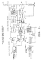
- the controller comprises a first supply portion which includes the functional blocks Logic With Isolation section 16, Oscillator section 18 and Current Sources section 20.
- a second control portion of the controller includes a MOSFET Drive and Current Limiting section 40, a MOSFET protection section 42, I 2 RC section 32, Logic section 44, Status section 34, Band Gap Current/Voltage section 30, Opto-Isolator Drive section 38 and a Power-up Reset section 36.
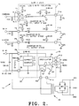
- a controller comprises two integrated circuits (ICs) referred to as Supply ASIC 12 and Control ASIC 14 and various discrete off-IC components.
- ICs integrated circuits
- the supply circuitry is made up of Supply Asic 12 and various off-IC components including capacitors, resistors, photo transistors/LEDs, transformers and diode bridges.
- Supply ASIC 12 is made up of functional sections Logic With Isolation 16, Oscillator 18 and Current Sources 20.
- the function of Logic With Isolation section 16 is to provide a TTL compatible input stage for a COMMAND line, an LED driver for the COMMAND line opto-isolator C, a TTL compatible output stage for STATUS and TRIP lines, and a photo-transistor receiver for STATUS and TRIP line opto-isolators S and T, respectively. All control signals communicated between ASICS 12 and 14 are passed through opto-isolators to achieve isolation between the two circuits.
- TTL input/output standards are as follows: Input TTL logic high input voltage 2.0V maximum TTL logic low input voltage 0.8V minimum TTL logic high input current 20u A maximum TTL logic low output current 400u A maximum Output TTL logic high output voltage 2.4V minimum TTL logic low output voltage 0.4V maximum TTL logic high output current 400u A minimum TTL logic low input current 8m A minimum
- the COMMAND input line is tied to an off-IC filter capacitor Ccd to protect against transient damage to ASIC 12 and connected to the input of invertor INV1 having hysteresis to improve noise immunity of the circuit.
- INV1 invertor
- the input of INV1 will be pulled high (one diode drop below BIAS) or low (one diode drop above BIAS GND), respectively in the event the COMMAND line is open circuited, i.e., disconnected.
- invertor INV1 When the input of invertor INV1 is high, the output of invertor INV1 is low, a saturated NPN transistor with 200u A current source from I3, and transistor Q1 is off (open collector) so that source I4 supplies current to the LED of the COMMAND opto-isolator C turning the LED on.
- Inverters INV2 and INV3 both have input stages incorporating hysteresis to improve the noise immunity of the circuits.
- Off-IC capacitor C tr and C st are tied to the TRIP and STATUS outputs respectively to protect against transient damage to the ASIC 12.
- the function of the oscillator section 18 is to produce a transformer drive signal which is used to power ASIC 14, the controller circuitry, by means of an isolation transformer 22, a full wave bridge BR1 and a smoothing capacitor C vs1 .
- Oscillator 26 is a standard emitter-coupled oscillator modified with high speed output comparators to drive transistors Q2 and Q3.
- the oscillator frequency is set by capacitor C osc and resistor R osc mounted externally of the ASIC.
- Oscillator 26 produces two output signals, A and B, which are 250 KHZ square waves 180° out of phase with each other.
- the oscillator outputs drive transistors Q2 and Q3 into saturation when high; the transistors having an open collector when low.
- the collector of transistors Q2 and Q3 are tied to the ends of the primary winding of transformer 22 whose center tap is connected to the BIAS line.
- the transformer acts as two synchronized 1:4 ratio transformers (1/2:2 primary to secondary ratio). With practical transformer efficiencies, saturation voltages of transistors Q2 and Q3 equal to 0.2V and a BIAS voltage of 5V, a 16.5V peak to peak square wave is produced across the transformer secondary.
- a full wave rectifier BR1 is placed across the transformer secondary to create a DC output of 15.1V.
- a capacitor C vs1 is placed across the DC outputs of the rectifier to smooth the output which is connected across VS1 and GND to power the control circuitry of ASIC 14.
- the function of the Current Sources section 20 is to provide temperature stable current sources to power other sections of the ASIC.
- the reference current level used to derive all other current sources is set by off-IC connected resistor R sbias .
- the current sources section 20 and other functional sections of ASIC 12 operate at a nominal voltage level of 5V.
- Off-IC capacitor C bias is added across the BIAS and BIAS GND lines to minimize noise generated by the switching of the functional blocks of ASIC 12 and to protect against transient damage to ASIC 12.
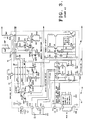
- the function of the control circuitry is to, a) turn the load current on and off by means of a solid state switch made up of MOSFETs in response to a C com input from ASIC 12, b) provide a primary trip mechanism to remove load current from the load in accordance with a selected trip time vs load current curve, c) limit the maximum load current to a predetermined calibrated level (current limit), d) provide a secondary trip mechanism that protects the MOSFETs from damage when in the current limiting mode, e) provide a trip latching feature which holds a trip, keeping the controller off until reset by the C com input from ASIC 12, f) provide the required drive signal for an opto-isolator LED to communicate a status indication to ASIC 12 reflecting that either load voltage or load current above a specified threshold is present, and g) provide the required drive signal for an opto-isolator LED to communicate a trip indication to ASIC 12.
- Control ASIC 14 is made up of Control ASIC 14 and various off-IC components including resistors, capacitors, photo-transistors/LEDs, MOSFETs and semiconductor transient suppressors.
- Control ASIC 14 comprises the following functional sections: Band Gap Current/Voltage Reference section 30, I 2 RC section 32, Status section 34, Power-Up-Reset section 36, Opto-Isolator Reference Drive section 38, MOSFET Drive and Current Limiting section 40, MOSFET Protection section 42 and Logic section 44.
- Band Gap Current/Voltage Reference section 30 provides a temperature stable voltage reference, temperature stable current sources and resistor ratioed current sources used by other functional sections within ASIC 14.
- V ref the band gap voltage reference
- BG temperature stable band gap
- RR resistor ratioed current sources
- I 2 RC circuit 32 creates an electronic analog of the temperature of a wire as a function of the heating due to current flow through the wire and outputs a trip signal indicating that the temperature of the wire has risen a predetermined amount, simulating a selected trip time vs load current curve.
- circuit 32 provides a feature known as "thermal memory". Thermal memory is a term which refers to the feature of shortening the trip time of a given load current level due to previously stored energy in the wire, or equivalently elevated initial wire temperature, as a result of previous load current flow. Without this feature, trip times for a given load current level would remain constant and repeated applications of load current at intervals which did not allow the wire temperature to return to ambient would cause the wire to exceed the maximum specified level.
- a thermal model of the wire can be used to determine the time required for a given amount of power dissipation to raise the wire temperature a selected amount.
- the I 2 RC circuit section 32 simulates the temperature rise of the wire and produces a trip signal when the temperature of the wire has risen a specified amount. Circuit 32 produces an electrical signal in the form of voltage which is proportional to the above energy/temperature equation in the manner described below.
- the non-inverting terminal of ground sensing op-amp OP2 is tied to the positive connection of shunt RS through resistor R24 of 600 ohms.
- the output of op-amp OP2 is connected to the base of NPN transistor Q29 and to ground through stabilizing capacitor C t1 and serially connected resistor R iv .
- the emitter of transistor Q29 is tied to the junction of capacitor C ti and resistor R iv and to the inverting terminal of op-amp OP2 through resistor R25 of 600 ohms. This arrangement in the feedback path of the op-amp OP2 forces the voltage of the inverting terminal of op-amp OP2 to equal the voltage at its non-inverting terminal, i.e., R s voltage.
- Calibration of current i2(t) provides a means of adjusting the ultimate trip of the controller trip time vs load current curve in a highly accurate, quick manner and at low cost.
- Ultimate trip calibration is performed by disconnecting capacitor C i , to be discussed below, from the circuit to make the time constant of the circuit equal to 0, running the selected ultimate trip current through the controller, and trimming resistors R t 1 and R t 2 until the voltage difference between pins C al 1 and C al 2 (P29, P30), connected respectively to the inverting and non-inverting inputs of comparator CMP7, is 0V. Capacitor C i is then connected to complete the circuit.
- resistor trimming procedures such as laser trimming, only increases the value of a resistor, two resistors are needed to adjust current i2(t). Increasing the value of R t 1 tied to transistor Q30 will increase i2(t) whereas increasing the value of R t 2 tied to transistor Q31 will decrease the value of current i2(t).
- the current to be squared, i2 is fed into diode connected transistors Q33, Q34.
- Transistor Q36 is fed by a relatively large current source I ref (300u A).
- I ref the large current source
- the diode drop across transistor Q36 is essentially constant and the total of the two V bes built-up across transistors Q33, Q34 is imposed across the base-emitter of transistor Q35 thereby squaring the Q33, Q34 collector current.
- V w (t) Y/C i I w (1 - e -t/R i C i )
- Diode connected transistor Q40 is connected to the RC network R i C i to prevent discharge of the RC network through other circuitry such as comparator CMP7, preserving thermal memory even when power is removed, thereby providing the same memory function as an electromechanical thermal circuit breaker.
- Diode connector transistor Q41 connected between V ref derived from the Current/Voltage Circuit 30 and the non-inverting input of comparator CMP7 provides compensation for the temperature effect on the voltage drop across transistor Q40.
- V cmp 7- V w (t) + V Q40, where VQ40 is the voltage drop across Q40.
- V cmp 7+ V ref + VQ41, where VQ41 is the voltage drop across Q41.
- Diode Q41 is forward biased by current source I15.
- V cmp 7- will be less than V cmp 7+ and the output of comparator CMP7 will be high signifying that the wire temperature has not risen above the selected amount and therefore, a trip condition is not present.
- V cmp 7- will be greater than V cmp 7+ and the output of comparator CMP7 will be low signifying that the temperature of the wire has risen the selected amount and that a trip condition is present.
- the output of comparator CMP7 is tied to input C of NAND gate NAND 4 through line I 2 RC TRIP.
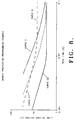
- off-IC component values used to achieve a trip time vs load current curve 2 per MS3320 seen in Fig. 4 are as follows:
- Dashed line curves 4 and 6 shown in Fig. 4 represent maximum and minimum trip time vs load current curves, respectively.
- V w (t) equation (Nos. 8 or 9) it can be seen that adjusting one or more of the off-IC components of circuit 32 can tailor the circuit performance to meet specific requirements of a given application.
- the current performance characteristics which can be changed by adjusting one or more external components are the trip time vs load current curve time constant, load current rating (i.e., 2.5 amp, 5.0 amp, 10.0 amp, etc.) and ultimate trip load current.
- trip time vs load current curve time constants can be obtained by adjusting capacitor C i and resistor R i
- other load current ratings can be used by adjusting R s
- the ultimate trip load current can be adjusted by resistors R t 1, R t 2 and R iv .
- the resistance of the shunt R s has been chosen such that 100% rated current, RI, produces 100m V across the shunt (100m V/100% rated current), i.e., a controller with a rated current of 10A would use a 10m ohm shunt.
- RI 100% rated current
- a controller with a rated current of 10A would use a 10m ohm shunt.
- other shunt resistances providing other scale factors may be chosen.
- Status circuit 34 is to provide an output of either a selected current or a voltage status indication when the load current or load voltage, respectively, exceeds a predetermined threshold.
- Current status indication is chosen by connecting pin P25 to pin P24 whereas voltage status is chosen by connecting pin P26 to pin P24.
- an 18 mV reference voltage tied to the inverting terminal of the ground sensing comparator CMP3 is set by resistor ratio current source I4 of 30u A and a 600 ohm resistor R2.
- Comparator CMP3 is designed to have approximately 4 mV of hysteresis to enhance noise immunity of the circuit.
- the non-inverting terminal of comparator CMP3 is tied to resistor R s through 600 ohm resistor R1.
- the inverting pin of comparator CMP4 is connected to the positive terminal of band gap current source I5 of 50 u A, to the cathode of diode connected NPN transistor Q1 and through pin P27 to R vstat and then to LINE GND.
- the non-inverting terminal of comparator CMP4 is tied to a voltage reference, V ref , derived from the Current/Voltage circuit 30.
- Comparator CMP4 is designed having approximately 0.5V of hysteresis for noise immunity enhancement.
- Power Reset circuit 36 The function of Power Reset circuit 36 is to reset/disable critical sections of the circuitry of ASIC 14 until sufficient operating voltage is present across VS1 (pin P21) and GND (pin P23) for proper operation.
- Circuit 36 functions such that current flows in the common base PNP current mirrors made up of Q2, Q3, R3 and R6 before any other current sources within ASIC 14.
- the MOSFET Protection circuit 42 With output signal MP at the saturation voltage of transistor Q8, the MOSFET Protection circuit 42, to be described
- collector voltage of transistor Q4 When the collector voltage of transistor Q4 is greater than V q 6 + V q 5, current from the collector of Q4 will flow into the base of transistor Q7 causing the collector-emitter of transistor Q7 to saturate and turning off transistor Q8 (open collector) causing transistor Q8 to have no effect on the operation of MOSFET Protection circuit 42.
- the collector voltage of transistor Q4 will be equal V q 6 + V q 5 when VS1 is approximately one additional diode drop higher (8.2 V total).
- Opto-Isolator Drive section 38 The function of Opto-Isolator Drive section 38 is to provide a means of re-routing the main current sources, which supply the majority of ASIC 14, through the LED portion of the trip T and status S opto-isolators when required. Circuit section 38 also establishes a voltage supply VS2 from which most of the components within ASIC 14 are powered.
- Voltage source VS2 is established by the zener voltage of NPN transistor Q10 (6.8V) plus a forward biased diode drop of NPN transistor Q11 (0.7V) added for temperature compensation for a total of approximately 7.5V.
- Band gap current source I6 (200u A) will saturate transistor Q14 whose collector is tied to band gap current source I7 (2m A). The Q14 collector current, current I7, and the base current, I6, will flow into VS2 to power a majority of the ASIC 14 electronics.
- invertor INV4 When the input of invertor INV4 is high, the output of the invertor will be low sinking all of the current from current source I6 causing a zener breakdown of zener diode Q12 which pulls the base of transistor Q14 approximately one diode drop below the emitter turning Q14 off. With transistor Q14 off, current source I7 will flow through the LED portion of the status opto-isolator S (pin P19) and flow through pin P20 into VS2 to provide power for a majority of the ASIC 14 electronics and indicate current flow or load voltage above the thresholds.
- MOSFET Drive and Current Limiting circuit section 40 The function of MOSFET Drive and Current Limiting circuit section 40 is to control the MOSFETs drain-source resistance by manipulating the MOSFETs gate-source voltage.
- the MOSFET control functions are designed to turn the MOSFETs on and off and to limit the peak current flow through the MOSFETs to a calibrated or selected level. Limiting the current prevents over-current conditions from damaging the MOSFETs.
- a plurality of MOSFETs PS1-PS7 being indicated in the figure, have their sources and drains connected in parallel with their gates connected respectively to 600 ohm gate resistors R8-R14.
- Resistors R8-R14 along with another 600 ohm resistor R15 connected to off-IC mounted capacitor C T through pin P38 (if required an eighth MOSFET, and a 15V zener diode, can be substituted for C t at pin 38), are connected to the junction between current sources I12 and I11 and to pin P47.
- Current sources I12 and I11 are connected between source VS1 and ground with current source I10 connected between VS1 and the output of op-amp OP1 whose output is adapted to control the state of energization of source I11.
- band gap current source I10 When the ENABLE of op-amp OP1 is low the output of the comparator is pulled high by the band gap current source I10 of 100u A turning on band gap current source I11 of 2.2m A.
- Band gap current source I12 sources 600u A and current source I11 sinks 2.2m A with a net of 1.6m A flowing from the MOSFET gates and capacitor C T through the 600 ohm resistor R8 through R15, discharging the MOSFET gates and capacitor C T .
- the voltage at the negative terminal of source I11, also the positive terminal of source I12 will be approximately one diode drop above ground GND.
- ASIC 14 includes outputs to drive eight MOSFETs directly, that is the gate of eight MOSFETs can be tied directly to outputs of resistors R8 through R15. If additional MOSFETs are desired output CG and off-IC gate resistors are required. Output CG, pin P47, is connected to capacitor C comp and then through pin P45 to the non-inverting terminal of op-amp OP1.
- a load current exceeding the current limit level may occur at two different times.
- the controller may turn on into the load current, in which case the circuit will limit the load current to the current limit level during turn on.
- an overload current may be applied to the controller while it is fully on, i.e., with the MOSFETs drain-source at low resistance. In this case a large degree of current overshoot will occur while the circuit lowers the MOSFETs gate-source voltage to raise the drain-source resistance.
- NPN transistor Q16 and emitter resistor R16 are connected between the MOSFET gates and ground with its base tied to the shunt R s through diode connected NPN transistors Q17, Q18.
- the inverting terminal of op-amp OP1 is tied to CL1 pin P46.
- the current limit level percentage is approximately equal to the voltage at CL1 in millivolts when a 100m V/100% rated current shunt is chosen as described supra. For example, 800m V at CL1 will cause the circuit to current limit at approximately 800% of rated load. If a shunt having a different resistance is chosen, the current limit percentage set by the voltage at CL1 must be adjusted accordingly.
- the current limit voltage is set by resistor ratio current source I13 of 30u A, resistors R17 of 7.2K ohms, R18 of 14.4K ohms, R cl 1 and R cl 2.
- Resistors R cl 1 and R cl 2 are connected off-IC at pins P44, P43 respectively and make up the emitter resistors of Wilson current mirror Q19, Q20, Q21 with the collector of transistor Q19 and base of transistor Q21 connected to current source I13 and the collector of transistor Q21 connected to the inverting terminal of op-amp OP1 and serially connected resistors R17, R18.
- resistor trimming procedures such as laser trimming
- two resistors are required to adjust the voltage at CL1.
- Increasing the value of R cl 2 will increase the voltage at CL1 whereas increasing the value of R cl 1 will decrease the voltage at CL1.
- Capacitor C t is included in the circuit to adjust the turn on and turn off time of the MOSFETs by adjusting the rate of rise and fall of the MOSFETs gate-source voltage.
- Stabilizing capacitor C comp is connected in the OP1 feedback path to minimize load current oscillations during current limiting.
- resistors R17 and R18 are tied to the inverting terminal of comparator CMP5 whose non-inverting terminal is connected to shunt R s through resistor R19 and whose output is connected to the Logic circuit section 44 through a line labeled MP ENA.
- the voltage divider formed by resistors R17 and R18 make the voltage at the inverting terminal of comparator CMP5 (CMP5-) equal to 2/3 of the current limit voltage V cl 1.
- comparator CMP5 When the voltage across the shunt is less than 2/3 V cl 1, the output of comparator CMP5 is low. When the voltage across the shunt exceeds 2/3 V cl 1, the output of the comparator is high. As mentioned above, the output of comparator CMP5 is tied to Logic circuit 44 and is used as one of the signals required to enable the MOSFET Protection Circuit 42 to be discussed below.
- Transient suppressors VTR1, VTR2 are added across LINE to LINE GND and LOAD to LINE GND respectively to protect the MOSFETs and certain circuitry from damage due to LINE and LOAD voltage transients and from LOAD voltage transients caused by switching inductive loads.
- the function of the MOSFET Protection Circuit 42 is to provide a secondary trip signal that indicates when the MOSFET junction temperature has risen a selected amount due to high levels of power dissipation which can occur during current limiting.
- the circuit also includes a thermal memory feature to prevent repeated applications of current limiting at intervals which would not allow the MOSFET junction temperature to return to ambient preventing the MOSFETs from exceeding the maximum junction temperature.
- the resistance of the MOSFETs drain-source is increased to limit the current to a predetermined level as described above.
- the controller and the load form a voltage divider where the voltage across the load is such that only the current limit level is passing through the load and the rest of the line voltage is dropped across the controllers' LINE-LOAD terminals.
- a thermal model of the MOSFET package system encompassing the MOSFETs, packaging materials, and attachment materials was used to determine the time required for a given power dissipation to raise the junction temperatures of the MOSFETs a selected amount.
- the circuit simulates the temperature of the MOSFETs and trips when the temperature of the MOSFETs has risen the selected amount.
- the allowable temperature rise is simply the maximum allowable junction temperature of the MOSFET (e.g., 150° C) minus the maximum operating temperature of the controller (e.g., 80° C).
- Circuit portion 42 produces an electrical signal in the form of a voltage that is proportional to the above energy/temperature equation in the manner described below.
- Resistor Rmv is connected to LINE and ground GND through serially connected Q22 and R20.
- imv(t) (Vline(t)-Vload(t) - VQ22)/(Rmv + R20), where: VQ22 is the voltage drop across diode connected transistor Q22.
- imv(t) (Vline(t)-Vload(t))/(Rmv + R20) - VQ22/(Rmv + R20)
- imv(t) V(t)/(Rmv + R20) - VQ22/(Rmv + R20)
- the error term is partially compensated for through selection of R mv , C mp and R mp .
- Diode Q28 prevents discharge of the R mp and C mp network through other circuitry (i.e., comparator CMP6) preserving thermal memory even in the event power is removed from ASIC 14.
- Diode connected transistor Q27 tied between the non-inverting terminal of comparator CMP6 and VREF provides compensation for the temperature effect on the voltage drop across diode Q28.
- V cmp 6- V mp (t) + VQ28, where VQ28 is the voltage drop across diode Q28.
- V cmp 6 + V ref + VQ27
- VQ27 the voltage drop across diode Q27.
- Diode Q27 is forward biased by current source I14.
- V cmp 6 - will be less than V cmp 6 + and the output of comparator CMP6 will be high signifying that the junction temperature of the MOSFETs has not risen the allowable amount and, therefore, a trip condition is not present.
- V cmp 6 - will be greater than V cmp 6 + and the output of the comparator will be low signifying that the junction temperature of the MOSFETs has risen the allowable amount and, therefore, a trip condition is present.
- circuit section 42 When MP is low (i.e., saturated transistors output of invertor INV1 of logic circuit 44 to be discussed below) circuit section 42 is disabled due to the fact that the imv(t) current is diverted through the MP line away from circuit section 42. However, when MP is high (open collector) circuit section 42 operates as described above since none of the imv(t) current will flow into the MP line.
- Logic circuit 44 uses the various input signals, i.e., MP ENA, MP TRIP, I 2 RC TRIP and the C com input from ASIC 12, and provides appropriate output signals, i.e., CMD, MP and TRP, required to coordinate the operation of the other functional circuit sections of ASIC 14.
- Logic circuit 44 also provides a trip latch feature in which a latch sets upon a trip indication, turning the controller off, and remains set until a reset signal is applied.
- the C com input is the only operator controllable input signal driven by the supply ASIC 12.
- the C com input has the following three functions:
- the C com signal, along with band gap current source 11 is tied to the inverting input of comparator CMP1 with the non-inverting input connected to V ref .
- Comparator CMP1 has approximately 0.5V hysteresis designed into it so that the lower threshold is V ref and the upper threshold is V ref + 0.5.
- the collector of photo-transistor C is tied to the C com pin P17. When the LED portion of the opto-isolator is off, no collector current flows through the photo-transistor and the inverting terminal of comparator CMP1 is pulled up by current source 11 to approximately one diode drop below VS2.
- comparator CMP1 When the voltage at the inverting terminal of comparator CMP1 is higher than the upper voltage threshold at the non-inverting terminal (V ref + 0.5V), the output of comparator CMP1 is low. When the LED portion of the opto-isolator is on, the photo-transistor is saturated with a collector current of 150u A pulling the inverting input of comparator CMP1 below the lower threshold voltage of the non-inverting input (V ref ) and forcing the output of CMP1 high. The output of CMP1 is tied to the B input of gate NAND 2 and the A input of gate NAND 3.
- Capacitor Clat is tied to the positive terminal of band gap current source I2, the negative terminal of band gap current source I3 and the inverting terminal of comparator CMP2.
- current source I2 When the output of gate NAND 4 is low, current source I2 is off and source I3 discharges capacitor Clat pulling it to approximately one diode voltage drop above GND.
- the inverting terminal of comparator CMP2 falls below the voltage at the non-inverting terminal (V ref ) the output of comparator CMP2 goes high.
- current source I2 is on and a net current of I2-I3 charges capacitor Clat pulling it to approximately one voltage drop below VS2.
- the set and reset time delay of the trip latch within logic circuit 44 is provided by off-IC mounted capacitor Clat.
- the set and reset time delay enhances noise immunity by making any noise spikes of a duration less than the set and reset time delays unable to change the state of the trip latch.
- comparator CMP2 (high) is also tied to the A inputs of NAND 1 and NAND 2.
- the input B of NAND 2 is low so that input A has no effect in this state.
- gate NAND 1 since the controller is off no voltage is developed across the shunt so that the output of comparator CMP5 is low.
- the output of NAND 1 then is high which is inverted to low through INV1 with the result that the MOSFET Protection section 42 is disabled.
- the latch In the off state the latch is reset, the MOSFET Drive and Current Limiting section is turned off, the TRIP signal is low and the MOSFET Protection section is disabled.
- the MOSFET Protection section is enabled only when the load current is greater than two thirds of the current limit level in order to avoid the possibility of nuisance tripping while the MOSFETs are turning on.
- NAND 3 With respect to NAND 3, whose input A is high since its input B, as stated in the description of the off state, it remains with a high output.
- the solid state power controller provides means for controlling load current through an isolated, solid state, high side switch (turn on and off), through a COMMAND input line.
- the controller provides a means for tripping in accordance with a specified trip time vs load current curve, for limiting current flow through the load and for protecting the solid state switch from damage due to excessive power dissipation during current limiting. Trip conditions are latched keeping the controller off until a reset signal is applied through the COMMAND input line.
- the controller also provides a STATUS output reflecting load voltage or current and trip output signals giving an indication of the state of the controller and the load.
- Table 1 COMMAND STATUS TRIP CONTROLLER CONDITION 0 0 0 Controller off/reset 1 0 0 Controller on, load current/voltage below circuit threshold 1 1 0 Controller on, load current/voltage above circuit threshold 1 0 1 Controller tripped
- Controllers made in accordance with the invention containing solid state sensors and switches coupled with integrated circuit logic can be conveniently disposed in a sealed package and can be remotely mounted near the load they are protecting resulting in significant reduced power line cable weight and bulk.
- the solid state components significantly increase switching life as compared to conventional circuit breakers.
- controllers provide a means for switching high voltage DC, due to the availability of high voltage solid state switch components, not available using mechanical approaches.
- Such controllers can provide computer controlled load switching while maintaining current overload protection, i.e., they follow selected trip time vs. load current curves such as the standard MS3320 trip time vs. load current relationships thereby enabling optimization of wire size and current rating.
- the STATUS and TRIP feedback allows continuous monitoring, e.g., via a computer, of each controller circuit.
- the STATUS can be configured to monitor voltage at the load output terminal or current flow through the controller.
- means are provided to facilitate in-application adjustment (programmability) of some of the features mentioned herein, by means external to the sealed package.
- these features include, but are not limited to, the I 2 RC circuit, the Current Limit circuit and MOSFET Protection circuit.
- the means for calibrating the performance of these features for a specific application has been described above.
- the following description relates to modifying the performance of the features through the use of external components connected outside of the sealed package. This enables the protection features of a single unit to be customized for the requirements of any one of various different circuits.
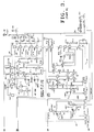
- I/O lines are added to the circuit of Fig. 5 to facilitate external programming.
- I/O lines are designated DTA, CLA1, CLA2 and MPA. Unlike control signals COMMAND, STATUS and TRIP these lines are not TTL compatible and are electrically referenced to ASIC 14.
- I/O line DTA is used in conjunction with the LOAD terminal to facilitate external programming of the I 2 RC circuit
- I/O lines CLA1 and CLA2 are used for external programming of the Current Limit level
- line MPA is used in conjunction with the LOAD terminal for external adjustment of the MOSFET Protection Circuit.
- the operation of the I 2 RC circuit is set by off-IC components R s , R iv , C t , R i and C i .
- R t1 and R t2 are used to calibrate the performance to the nominal set point (see Fig. 3).
- R i and C i are used to set the shape of the trip time vs. load current curve, similar to Fig. 4.
- Resistor R i is used to set the ultimate trip level and R i and C i together determine the time constant.
- the component values are sized to create a curve which is analogous to the temperature rise of the circuit wire.
- I 2 RC performance modification can be accomplished with the proper selection of R i and C i .
- R i and C i are segmented into R ii , C ii (internal to the package) and R ie , C ie (external to the package).
- R ie and C ie are connected in parallel to R ii and C ii by connecting R ie and C ie between I/O line DTA and the LOAD terminal.
- the DTA line is connected to R ii and C ii at P31 as shown in Fig. 6.
- the ground side of R ii and C ii is electrically connected to the LOAD terminal therefore the LOAD terminal is used as the return for R ie and C ie to reduce the total number of I/O pins required.
- R ii and C ii are used as default values and fix the lower limits of programmability.
- R ii fixes the lower limit of ultimate trip, C ii along with R ii fix the lower limit of the trip delay.
- the Current Limit level is made externally programmable as well.
- the Current Limit level is effected by off-IC components R s , R cl1 and R cl2 (see Fig. 3) in the manner developed above.
- R cl1 and R cl2 are used to set the Current Limit level during the calibration process.
- Calibration is normally accomplished by laser trimming of thick film resistors. Because laser trimming of resistors can only increase the resistance R cl1 and R cl2 are used to allow for an increase or decrease in the Current Limit level.
- V cl1 648 mV ⁇ (R cl2 /R cl1 )
- resistor R cl1 External programming is achieved by segmenting resistor R cl1 into two parallel resistors. One internal to the package R cl1i and a second programming resistor external to the package R cl1e . Resistor R cl1e is connected between I/O lines CLA1 and CLA2. CLA1 is connected to one end of R cl1i and ASIC 14 at P44 as shown in Fig. 6. CLA2 is connected to the other end of R cl1i and ASIC 14 at the secondary supply level of VS2 (P51). Practical limitations of ASIC 14 require that R cl1i and R cl2 not exceed 40 K Ohms. It is also desirable for device safety to make the default (no external component) current limit value the lowest value in the desired range.
- R CI1i is set to its maximum value of 40 K Ohms and R cl2 to the appropriate value to achieve the lowest current limit level desired. Placing this external resistor R cl1e in parallel with the internal resistor R cl1i will result in a lower "effective" R cl1 value which will result in an increase in the current limit level.
- R cl1e (R cl1i ⁇ R cl1 ) / (R cl1i - R cl1 )
- This feature is important in maximizing the power controller's ability to operate in reactive load circuits.
- the load characteristics are known to be low in reactance or are purely resistive so it may be desirable to shorten the time which the device will current limit before the trip occurs. It is also necessary to modify the MOSFET Protection ultimate trip level when the current limit level is adjusted through programming. It is desirable to have the MOSFET Protection ultimate trip level set just above the voltage produced by current flow equal to the current limit level. This requires that the MP ultimate trip level move up and down with the programmed current limit level.
- the MOSFET Protection performance can be modified by the proper selection of R mp and C mp .
- R mp and C mp must be segmented into R mpi , C mpi (internal to the package) and R mpe , C mpe (external to the package).
- R mpe and C mpe are connected in parallel to R mpi and C mpi by connecting R mpe and C mpe between I/O line MPA and the LOAD terminal.
- the MPA line is connected to R mpi and C mpi at P49 as shown in Fig. 6.
- the ground side of R mpi and C mpi is electrically connected to the LOAD terminal therefore the LOAD terminal is used as the return for R mpe and C mpe to reduce the total number of I/O pins required.
- R mpi and C mpi are used as default values and fix the lower limits of programmability.
- R mpi fixes the lower limit of ultimate trip and C ii along with R ii fix the lower limit of the trip delay. Because higher current limit levels are associated with higher power dissipation (faster junction temperature rise) the default settings are not likely to be used at the same time. A high current limit level would require a high ultimate trip setting and a short trip delay (time constant) while a low current limit level would require a low ultimate trip but could allow a longer trip delay.
- Curve C is used for a device with the current limit level programmed to 400% of the rated current while curve D is used for the same device with the current limit level programmed to 1200%. It is determined that the LINE to LOAD voltage drop developed when 400% current flow is 2 V while the voltage drop is 6 V at 1200%. Therefore, for curve C the ultimate trip level will be set for 2.5 V and at 7 V for curve D.
- the maximum time constants for these curves are a function of the thermal properties of the MOSFETs and their packaging environment. For this example, the maximum time constant of curve C is 52 mS while for curve D it is 4.3 mS.
- a controller made in accordance with the invention also provides current limiting and power switch protection.
- the controller limits the circuit current to a present level and maintains it, tripping only when the power switch junction temperature has risen the selected amount thereby avoiding premature tripping due to momentary transients.
Landscapes
- Emergency Protection Circuit Devices (AREA)
- Control Of Voltage And Current In General (AREA)
- Protection Of Static Devices (AREA)
Description
- This invention relates generally to a solid state circuit controller and more specifically to a solid state circuit controller for switching power to a load and for protecting the switch from damage due to power dissipation. Document DE-A-4005813 discloses such a controller having the features of the preamble of
claim 1. - The controller has utility in many applications, such as, by way of example, in aircraft power distribution systems. Traditionally, such systems have been controlled with electromechanical circuit breakers incorporating a bimetallic element to sense the resistive heating of wire due to current flow. A key inherent quality of the bimetallic sensor is known as "thermal memory". The bimetal stores and dissipates the heat energy in the same manner as the wire and reduces circuit breaker trip time when the wire temperatures remain elevated from a previous overload condition. This protects the wire when exposed to multiple overloads or preload conditions by maintaining the heat energy below the threshold for wire damage as set forth in MS3320 trip time vs. load current curve standard. Such circuit breakers also allow momentary high inrush currents such as motor loads and lamp loads without nuisance tripping. For example, inrush currents of four to fifteen times nominal rating, some lasting several seconds, are typical of motors, power supplies and incandescent filaments.
- Advances in solid state and computer technology now offer the potential for fully automatic control resulting in reduced flight crew overload, enhanced maintainability and reliability as well as significant weight savings. One approach in providing such a control is shown and described in U.S. Patent No. 4,866,559 assigned to the assignee of the present invention. In that control an electrothermal sensor is used as a current sensing element. The I2RC power dissipation within a resistive beam of the current sensing element provides a measurable temperature gradient across its surface as a function of current flow and time. An electronic circuit responds to a maximum temperature difference between the center and the edge of the beam resulting in a trip time vs. load current trip characteristic similar to the traditional electromechanical, thermal circuit breakers.
- While this approach is effective, the space required for the electromechanical sensor is greater than desirable and the fabrication process employed to maintain the required optimum performance relative to temperature is costly.
- It therefore an object of the present invention to provide an improved solid state power controller which includes the performance characteristics of traditional thermal circuit breakers which overcomes the above noted problems of the prior art. Another object is the provision of a solid state power controller having improved accuracy as well as one which is compatible with hybrid manufacturing practices and which is conducive for use with computer control systems. Yet another object is the provision of a solid state power controller which is easily adaptable to a wide variety of applications such as different time current curves, load current curves and the like. Another object is the provision of a solid state controller which can be used for switching high voltage DC.
- It is another object of the present invention to provide protection of solid state switches used in such power controllers, such as MOSFETs, from thermal damage due to power dissipation. Another object is the provision of controller apparatus to protect solid state power switches used to limit current flow therethrough, as well as to switch high voltage DC, from thermal damage from power dissipated in the switches.
- Yet another object of the present invention to provide in-situ, external programmability of a solid state controller in order to allow adjustment of certain features including current overload protection, MOSFET thermal protection and current limit as desired for different applications.
- Various other objects and advantages will appear from the following description of an embodiment of the invention and the novel features will be particularly pointed out hereinafter in connection with the accompanying drawings and the appended claims.
- According to the present invention there is provided a solid state controller for controlling current through a wire to a load by means of a solid state switch means through an input line having
- a low resistance shunt resistor serially connected to the solid state switch means and a wire connecting the switch means to the load,
- means for measuring the voltage drop across the shunt resistor, and
- means having a signal proportional to the current flowing through the shunt resistor as an input signal to be compared to reference values to limit current flow through the solid state switch means to a selected value while continuing to permit current flow,
- In one embodiment of the present invention, there is provided a controller comprising two integrated circuits referred to as a Supply ASIC and a Control ASIC along with various discrete external components including resistors, capacitors, a transformer, zener diodes, MOSFETs and the like.
- The Supply ASIC comprises a Current Sources section, a Logic With Isolation section and an Oscillator section.
- The Logic With Isolation section provides an interface between the external controller and the Control ASIC circuitry and has a COMMAND input and STATUS and TRIP output stages fully TTL compatible. The input COMMAND signal controls the on/off and trip reset functions. In the event that the external COMMAND signal is removed as by being open circuited due to harness wire breakage, a default COMMAND high (controller on) or low (controller off) condition can be set by connecting the COMMAND input to a normally closed pin or a normally open pin respectively. The output STATUS signal reflects whether or not a selected load current or load voltage status exists while an output TRIP signal reflects whether or not a trip condition has occurred. A trip condition can be caused by either an I2RC circuit or a MOSFET Protection circuit, to be discussed below.
- The Current Sources section provides temperature stable current sources for the Supply ASIC Logic with isolation section and the Oscillator section. Bias currents are set by an external resistor.
- The Oscillator section produces a drive signal for a transformer which in turn is used to power the isolated Control ASIC circuitry. The oscillator is made up of a modified emitter coupled oscillator with high speed comparator outputs. Frequency of the oscillator is set by an externally mounted resistor and capacitor.
- The Control ASIC may comprise a MOSFET Drive and Current Limiting section a MOSFET Protection section, an I2RC section, a Logic section, a Status section, a Band Gap Current/Voltage Reference section, an Opto-Isolator Drive section and a Power-Up-Reset section.
- The MOSFET Drive and Current Limiting section turns MOSFETs on and off by controlling MOSFET gate-source voltage. Additionally, this section may limit current flow through the MOSFETs to a predetermined level by decreasing and increasing the MOSFETs on resistance through increasing and decreasing the gate-source voltage, respectively. External calibration of the current limit level is effected by trimming a pair of externally mounted resistors. The controller preferably employs N-channel MOSFETs since they have lower on-resistance than comparable sized P-channel MOSFETs.
- The MOSFET Protection section produces an analog voltage proportional to the MOSFET temperature rise and provides a trip signal when the allowable temperature rise of the MOSFETs, simulated by a reference voltage, is reached in order to protect the MOSFETs from thermal damage caused by high power dissipation during current limiting. The MOSFET protection section may include thermal memory.
- A current is generated proportional to the voltage drop across the MOSFET which is converted to a first electrical signal proportional to the power dissipated in the MOSFET. This signal is integrated as a function of time providing a second signal proportional to the temperature rise of the junction of the MOSFET and a trip signal is generated when the preselected allowable temperature rise of the junction has been reached.
- The I2RC section produces an analog voltage proportional to the wire temperature rise or equivalently energy stored in the wire and produces a trip signal when the maximum temperature rise of the wire, simulated by a reference voltage, is reached. The section comprises a linear circuit which measures the current flow through the wire, calculates its heating impact on the wire and provides a signal to trip the controller when the wire temperature has risen a selected amount as defined by a selected curve set such as one derived from the MS3320 trip time vs. load current curves. The circuit reads the current in the wire as a voltage signal across a shunt resistor serially connected to the wire, the signal is scaled and converted to a current by an amplifier state, then squared with the resultant applied to an RC network. The output voltage from the RC network is monitored by a comparator which has a threshold set by the referenced voltage according to the energy equation. When the output voltage of the RC network reaches the threshold level, the comparator output transitions to an opposite state signalling Logic section of a trip condition in order to interrupt current flow within the wire by turning off the MOSFETs. The I2RC section may include thermal memory.
- The Logic section produces internal control signals for the MOSFET Drive and Current limiting section, MOSFET Protection section and Optoisolator Drive section based on COMMAND input and trip signals from the I2RC section and MOSFET Protection section. This section may also contain a trip latch to hold a trip condition until a reset is applied by the COMMAND input signal. The trip latch contains a set and reset delay to prevent false tripping and resetting from induced voltage or current spikes. The delay can be adjusted by an externally mounted capacitor.
- The Status section provides a signal indicating whether the voltage at the LOAD terminal, if the voltage status is chosen, or the old current, if the current status is chosen, exceeds predetermined levels. Hysteresis is employed with both voltage and current status thresholds to enhance noise immunity. The voltage status thresholds with hysteresis are set by an external resistor whereas the current status thresholds with hysteresis are internally set.
- The Band Gap Current/Voltage Reference section provides a temperature stable voltage reference and current sources to operate the other sections of the Control ASIC circuitry. This section also provides current sources whose values are ratioed to internal ASIC resistors. The ratioed resistor current sources are used to establish temperature stable voltages, other than the voltage reference, within the sections of the Control ASIC. The voltage reference and current sources are established through the use of an inherently temperature stable "band gap voltage" reference. Band Gap current source values are set by an external resistor. The band gap voltage reference is also used to establish a supply voltage of approximately 7.5 V used by other sections of the ASIC.
- The Opto-Isolator Drive section provides the drive signal for opto-isolator photo diodes to transmit status and trip indications to the Supply ASIC. To turn a photo diode on, indicating a status or trip condition, the circuit diverts the 7.5 V supply current through an opto-isolator photo diode.
- The Power-Up-Reset section sets the functional sections of the control circuitry to a predetermined state such as MSOFETS off, trip latch reset, trip and status opto-isolator off, MOSFET protection disabled and the like until there is sufficient supply voltage to operate the Control ASIC.
- Selected features of the controller may be made externally programmable to facilitate customizing the controller in-situ for a particular application. These features include the I2RC circuit, the Current Limit circuit and the MOSFET Protection circuit by calibrating the features to a default level and by adding lines extending out of the sealed package containing the controller to external connecting points. The operation of the I2RC circuit is set by certain components disposed off the integrated circuits (ICs) comprising the controller circuitry including a resistor Ri and capacitor Ci used to set the shape of the trip time vs. load current curve where resistor Ri is used to set the ultimate trip level and Ri and Ci together determine the time constant. Ri and Ci may be segmented into Rii, Cii (disposed internally in the package) and Rie, Cie (disposed externally outside the package). Rie and Cie are connected in parallel to Rii and Cii. The internal, off-IC components Rii and Cii are selected to provide default values and to fix the lower limits or programmability.
- The current level may also be externally programmable. The current limit level is affected by off-IC resistors Rs, Rc11 and Rc12. Resistor Rc11 is segmented into two parallel resistors with Rc11i disposed within the package and Rc11e disposed outside the package between external connection points on current paths extending out of the sealed package. The value of resistors Rc11i and Rc12 selected to a default level, the lowest current limit value in the desired range. Placing external resistor Rc11e in parallel with internal resistor Rc11i will result in a lower effective Rc11 value and increase the value the current limit level.
- The MOSFET Protection circuit may be externally programmable in a manner similar to the I2RC circuit. Operation of the MOSFET Protection circuit is set by off-IC components, resistors Rmv, Rmp and capacitor Cmp. Components Rmp and Cmp are used to set the shape of the trip time vs. LINE to LOAD voltage with resistor Rmp used to set the ultimate trip level and components Rmp and Cmp together determining the time constant. Resistor Rmp and capacitor Cmp are segmented into Rmpi, Cmpi disposed internally in the package and Rmpe, Cmpe disposed externally of the package. Rmpe and Cmpe are connected in parallel to Rmpi and Cmpi and the values of Rmpi and Cmpi are chosen as default values to fix the lower limits of programmability.
-
- Fig. 1 is a block diagram of a solid state circuit controller made in accordance with the invention;
- Fig. 2 is a circuit diagram showing a Supply ASIC and associated off-IC components used with the present invention;
- Fig. 3 (parts A and B) is a circuit diagram showing the Control ASIC and associated off-IC components used with the present invention;
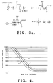
- Fig. 3a shows several conventional symbols and their equivalents;
- Fig. 4 is a trip time vs load current curve as used in accordance with the present invention.
- Fig. 5 is a block diagram of a solid state circuit controller similar to Fig. 1 but showing additional lines used for programming the controller;
- Fig. 6 (parts A and B) is a circuit diagram similar to Fig. 3 but showing internal default components, programming points and external programming components;
- Fig. 7 is similar to Fig. 4 but shows a programming range for trip time vs. load current values; and
- Fig. 8 shows Line to Load Voltages vs. Trip Time switch protection curves.
- With particular reference to Fig. 1 the controller comprises a first supply portion which includes the functional blocks Logic With
Isolation section 16,Oscillator section 18 andCurrent Sources section 20. A second control portion of the controller includes a MOSFET Drive and Current Limitingsection 40, aMOSFET protection section 42, I2RC section 32,Logic section 44,Status section 34, Band Gap Current/Voltage section 30, Opto-Isolator Drive section 38 and a Power-upReset section 36. - With reference to the following description it should be noted that all current sources are non-ideal. They are only functional provided the negative terminal of the current source is approximately one diode voltage drop above the positive terminal. If there is less than one diode drop, the output current is effectively zero. Unless otherwise noted, the outputs of each logic gate and comparator is an open collector transistor (NPN), therefore a logic low voltage is equal to the saturation voltage of the output transistor (approximately 0.2V). The inputs of all logic gates are non-ideal current sources, therefore, due to the non-ideal behavior of the current sources a logic high voltage is equal to the voltage at the negative terminal of the current source minus one diode voltage drop. Unless otherwise stated, all voltages within an ASIC are referenced to the local or individual ASIC ground. The stated voltages are assumed to be nominal.
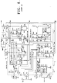
- According to a preferred embodiment of the invention, as seen in Figs. 2 and 3, a controller comprises two integrated circuits (ICs) referred to as
Supply ASIC 12 andControl ASIC 14 and various discrete off-IC components. - As seen in Fig. 2, the supply circuitry is made up of
Supply Asic 12 and various off-IC components including capacitors, resistors, photo transistors/LEDs, transformers and diode bridges.Supply ASIC 12 is made up of functional sections Logic WithIsolation 16,Oscillator 18 andCurrent Sources 20. - The function of Logic With
Isolation section 16 is to provide a TTL compatible input stage for a COMMAND line, an LED driver for the COMMAND line opto-isolator C, a TTL compatible output stage for STATUS and TRIP lines, and a photo-transistor receiver for STATUS and TRIP line opto-isolators S and T, respectively. All control signals communicated betweenASICS - TTL input/output standards are as follows:
Input TTL logic high input voltage 2.0V maximum TTL logic low input voltage 0.8V minimum TTL logic high input current 20u A maximum TTL logic low output current 400u A maximum Output TTL logic high output voltage 2.4V minimum TTL logic low output voltage 0.4V maximum TTL logic high output current 400u A minimum TTL logic low input current 8m A minimum - The COMMAND input line is tied to an off-IC filter capacitor Ccd to protect against transient damage to
ASIC 12 and connected to the input of invertor INV1 having hysteresis to improve noise immunity of the circuit. Depending on the particular load with which the controller is to be used, by tying either the normally closed current source I1 of 10u A or the nominally open current source I2 of 10u A pin to the COMMAND pin, the input of INV1 will be pulled high (one diode drop below BIAS) or low (one diode drop above BIAS GND), respectively in the event the COMMAND line is open circuited, i.e., disconnected. - Current sources I3 and I4 are connected to the base and collector respectively of transistor Q1 whose collector is also connected to opto-isolator C. When the input of invertor INV1 is low the output of invertor INV1 is an open collector NPN transistor and I3 of 200u A supplies base current to transistor Q1. Transistor Q1 is saturated with a collector current of 2m A supplied by I4, therefore no current flows through the LED of the COMMAND opto-isolator C and the LED is off.
- When the input of invertor INV1 is high, the output of invertor INV1 is low, a saturated NPN transistor with 200u A current source from I3, and transistor Q1 is off (open collector) so that source I4 supplies current to the LED of the COMMAND opto-isolator C turning the LED on.
- Inverters INV2 and INV3 both have input stages incorporating hysteresis to improve the noise immunity of the circuits. Off-IC capacitor Ctr and Cst are tied to the TRIP and STATUS outputs respectively to protect against transient damage to the
ASIC 12. - When the state of the photo-transistor of the TRIP opto-isolator T is open collector (LED off), the input of invertor INV2 is pulled above the upper threshold by I5 (200u A) and the output of invertor INV2 goes low, a saturated NPN transistor, signifying no trip condition. When the photo-transistor of the TRIP opto-isolator T is saturated (LED on) the input of invertor INV2 is below the lower threshold and the output of invertor INV2 is an open collector NPN transistor and is pulled high by I8 of 800u A signifying a trip condition.
- In like manner, when the state of the photo-transistor of the STATUS opto-isolator S is an open collector (LED off), the input of invertor INV3 is pulled above the upper threshold by current source I6 (200u A) and the output of invertor INV3 goes low, a saturated NPN transistor, signifying no status condition. When the photo-transistor of the STATUS opto-isolator is saturated (LED on), the input of invertor INV3 is below the lower threshold and the output of INV3 is an open collector NPN transistor and is pulled high by I7 of 800u A signifying a status condition.
- The function of the
oscillator section 18 is to produce a transformer drive signal which is used to powerASIC 14, the controller circuitry, by means of anisolation transformer 22, a full wave bridge BR1 and a smoothing capacitor Cvs1. -
Oscillator 26 is a standard emitter-coupled oscillator modified with high speed output comparators to drive transistors Q2 and Q3. The oscillator frequency is set by capacitor Cosc and resistor Rosc mounted externally of the ASIC.Oscillator 26 produces two output signals, A and B, which are 250 KHZ square waves 180° out of phase with each other. The oscillator outputs drive transistors Q2 and Q3 into saturation when high; the transistors having an open collector when low. The collector of transistors Q2 and Q3 are tied to the ends of the primary winding oftransformer 22 whose center tap is connected to the BIAS line. Driven by transistors Q2 and Q3 the transformer acts as two synchronized 1:4 ratio transformers (1/2:2 primary to secondary ratio). With practical transformer efficiencies, saturation voltages of transistors Q2 and Q3 equal to 0.2V and a BIAS voltage of 5V, a 16.5V peak to peak square wave is produced across the transformer secondary. A full wave rectifier BR1 is placed across the transformer secondary to create a DC output of 15.1V. A capacitor Cvs1 is placed across the DC outputs of the rectifier to smooth the output which is connected across VS1 and GND to power the control circuitry ofASIC 14. - The function of the
Current Sources section 20 is to provide temperature stable current sources to power other sections of the ASIC. The reference current level used to derive all other current sources is set by off-IC connected resistor Rsbias. Thecurrent sources section 20 and other functional sections ofASIC 12 operate at a nominal voltage level of 5V. Off-IC capacitor Cbias is added across the BIAS and BIAS GND lines to minimize noise generated by the switching of the functional blocks ofASIC 12 and to protect against transient damage toASIC 12. - The function of the control circuitry is to, a) turn the load current on and off by means of a solid state switch made up of MOSFETs in response to a Ccom input from
ASIC 12, b) provide a primary trip mechanism to remove load current from the load in accordance with a selected trip time vs load current curve, c) limit the maximum load current to a predetermined calibrated level (current limit), d) provide a secondary trip mechanism that protects the MOSFETs from damage when in the current limiting mode, e) provide a trip latching feature which holds a trip, keeping the controller off until reset by the Ccom input fromASIC 12, f) provide the required drive signal for an opto-isolator LED to communicate a status indication toASIC 12 reflecting that either load voltage or load current above a specified threshold is present, and g) provide the required drive signal for an opto-isolator LED to communicate a trip indication toASIC 12. - As seen in Fig. 3, the control circuitry is made up of
Control ASIC 14 and various off-IC components including resistors, capacitors, photo-transistors/LEDs, MOSFETs and semiconductor transient suppressors.Control ASIC 14 comprises the following functional sections: Band Gap Current/Voltage Reference section 30, I2RC section 32,Status section 34, Power-Up-Reset section 36, Opto-IsolatorReference Drive section 38, MOSFET Drive and Current Limitingsection 40,MOSFET Protection section 42 andLogic section 44. - Band Gap Current/
Voltage Reference section 30 provides a temperature stable voltage reference, temperature stable current sources and resistor ratioed current sources used by other functional sections withinASIC 14. - Vref, the band gap voltage reference, is derived from a standard band gap reference circuit which creates an inherently temperature stable voltage of approximately 1.25V which is scaled up using internal resistor rationing to obtain Vref of 3.25V which serves as a reference voltage for other functional blocks of
ASIC 14. Vref is also used in conjunction with Rcbias to create temperature stable band gap, BG, current sources used to power other functional blocks withinASIC 14. Resistor ratioed, RR, current sources are also developed within this section whose values are ratioed by internal ASIC resistors to create temperature stable voltage references of values other than Vref, needed by other functional sections ofASIC 14, by feeding the RR current sources through internal ASIC resistors matched with those used to establish the value of the RR current sources. - I2RC circuit 32 creates an electronic analog of the temperature of a wire as a function of the heating due to current flow through the wire and outputs a trip signal indicating that the temperature of the wire has risen a predetermined amount, simulating a selected trip time vs load current curve. In addition,
circuit 32 provides a feature known as "thermal memory". Thermal memory is a term which refers to the feature of shortening the trip time of a given load current level due to previously stored energy in the wire, or equivalently elevated initial wire temperature, as a result of previous load current flow. Without this feature, trip times for a given load current level would remain constant and repeated applications of load current at intervals which did not allow the wire temperature to return to ambient would cause the wire to exceed the maximum specified level. - A thermal model of the wire can be used to determine the time required for a given amount of power dissipation to raise the wire temperature a selected amount. The following first order differential equation models the energy stored in the wire as a function of time (Ew(t)) which is proportional to the temperature rise of the wire as a function of time:

- Rw
- resistance of the wire.
- Iw(t)
- current through the wire as a function of time.
- Rw Iw 2(t)
- power dissipated within the wire
- K
- 1/ the thermal time constant of the wire.
- The solution is as follows:

- Ew(t=0)e-Kt
- the thermal memory of the equation where Ew(t=0) is the energy stored in the wire at time = 0.
- The I2
RC circuit section 32 simulates the temperature rise of the wire and produces a trip signal when the temperature of the wire has risen a specified amount.Circuit 32 produces an electrical signal in the form of voltage which is proportional to the above energy/temperature equation in the manner described below. - Load current Iw(t) flowing through shunt Rs causes a voltage to be developed across shunt Rs as follows:


emitter resistors R t1 andR t2 for transistors Q30 and Q31 respectively provide a means for external calibration of current i2(t). That is,
resistors R t1 andR t2 until the voltage difference between pins Cal 1 and Cal 2 (P29, P30), connected respectively to the inverting and non-inverting inputs of comparator CMP7, is 0V. Capacitor Ci is then connected to complete the circuit. - Due to the fact that resistor trimming procedures such as laser trimming, only increases the value of a resistor, two resistors are needed to adjust current i2(t). Increasing the value of
R t1 tied to transistor Q30 will increase i2(t) whereas increasing the value ofR t2 tied to transistor Q31 will decrease the value of current i2(t). - NPN transistors Q33, Q34, Q35, Q36 and current source Iref, a band gap current source of 300u A, form an approximate current squaring function as follows:

- The current to be squared, i2, is fed into diode connected transistors Q33, Q34. Transistor Q36 is fed by a relatively large current source Iref (300u A). As a result of the large current source (Iref) relative to i3 the diode drop across transistor Q36 is essentially constant and the total of the two Vbes built-up across transistors Q33, Q34 is imposed across the base-emitter of transistor Q35 thereby squaring the Q33, Q34 collector current.
- Transistors Q37, Q38, Q39 and resistors R26 and R27 form a standard Wilson current mirror configuration providing improved collector current matching by minimizing base current error with emitter resistors to minimize errors due to transistor Vbe mismatch resulting in:

- Current i4(t) flows through diode connected NPN transistor Q40 to charge the parallel R-C network made-up of resistor Ri and capacitor Ci. The voltage across resistor Ri and capacitor Ci is as follows:


- By comparing the equations for Ew(t), No. 2, and Vw(t), Nos. 8 or 9, it can be seen that the two are proportional under the following conditions:
- Ri Ci = 1/K, setting the time constants of the two equations equal to each other,
- I4(t) is proportional to Iw 2(t) as shown previously by equation Nos. 6 and 7, and
- 1/Ci * Y (constant) is chosen to be the right proportion to Rw.
- By way of example, let Iw(t) be a step function (Iw(t) = Iw for t > 0, Iw(t)=0 for t < 0) and Vw(t = 0) = 0, then the solution for Vw(t) is:

- It may be noted that this equation is used to develop the Fig. 4 curve.
- Diode connected transistor Q40 is connected to the RC network Ri Ci to prevent discharge of the RC network through other circuitry such as comparator CMP7, preserving thermal memory even when power is removed, thereby providing the same memory function as an electromechanical thermal circuit breaker.
- Diode connector transistor Q41 connected between Vref derived from the Current/
Voltage Circuit 30 and the non-inverting input of comparator CMP7 provides compensation for the temperature effect on the voltage drop across transistor Q40. - The voltage at the inverting terminal of CMP7 (Vcmp 7-) is equal to:
Vcmp 7- = Vw(t) + V Q40, where VQ40 is the voltage drop across Q40. - The voltage at the non-inverting terminal of CMP7(
V cmp 7+) is equal to:
V cmp 7+ = Vref + VQ41, where VQ41 is the voltage drop across Q41. Diode Q41 is forward biased by current source I15. - Assuming that the difference between the voltage drop across VQ40 and VQ41 is negligible, when Vw(t) is less than Vref then Vcmp 7- will be less than
V cmp 7+ and the output of comparator CMP7 will be high signifying that the wire temperature has not risen above the selected amount and therefore, a trip condition is not present. - Again, assuming that the difference between the voltage drop across VQ40 and VQ41 is negligible, when Vw(t) is greater than Vref, Vcmp 7- will be greater than
V cmp 7+ and the output of comparator CMP7 will be low signifying that the temperature of the wire has risen the selected amount and that a trip condition is present. The output of comparator CMP7 is tied to input C ofNAND gate NAND 4 through line I2RC TRIP. - As an example, off-IC component values used to achieve a trip time vs load
current curve 2 per MS3320 seen in Fig. 4 are as follows: - Rs =
- 10m ohm (10.0 amp rated load current)
- Riv =
- 15.8 K ohm
- Ct =
- 1000 pF
- Ri =
- 15.1 M ohm
- Ci =
- 1 uF
-
R t1 andR t2 = - Adjusted to set the nominal ultimate trip load current percentage (126.5 of rated current). Approximate value for each of
R t1 andR t2 is 20 K ohms. - Dashed line curves 4 and 6 shown in Fig. 4 represent maximum and minimum trip time vs load current curves, respectively.
- Using the Vw(t) equation (Nos. 8 or 9) it can be seen that adjusting one or more of the off-IC components of
circuit 32 can tailor the circuit performance to meet specific requirements of a given application. The current performance characteristics which can be changed by adjusting one or more external components are the trip time vs load current curve time constant, load current rating (i.e., 2.5 amp, 5.0 amp, 10.0 amp, etc.) and ultimate trip load current. For example, for a given load current rating, other trip time vs load current curve time constants can be obtained by adjusting capacitor Ci and resistor Ri, for a given trip time vs load current curve time constant, other load current ratings can be used by adjusting Rs, the ultimate trip load current can be adjusted byresistors R t1,R t2 and Riv. - Preferably, the resistance of the shunt Rs has been chosen such that 100% rated current, RI, produces 100m V across the shunt (100m V/100% rated current), i.e., a controller with a rated current of 10A would use a 10m ohm shunt. By choosing the shunt in this way, the voltage produced across the shunt for a given rated current percentage will be the same independently of the rated current value, e.g, x % of R I = x mV across Rs. However, if desired, other shunt resistances providing other scale factors may be chosen.
- The function of
Status circuit 34 is to provide an output of either a selected current or a voltage status indication when the load current or load voltage, respectively, exceeds a predetermined threshold. Current status indication is chosen by connecting pin P25 to pin P24 whereas voltage status is chosen by connecting pin P26 to pin P24. With respect to the current status, an 18 mV reference voltage tied to the inverting terminal of the ground sensing comparator CMP3 is set by resistor ratio current source I4 of 30u A and a 600 ohm resistor R2. Comparator CMP3 is designed to have approximately 4 mV of hysteresis to enhance noise immunity of the circuit. The non-inverting terminal of comparator CMP3 is tied to resistor Rs through 600 ohm resistor R1. When the voltage across shunt Rs is less than the lower threshold of CMP3 (18 mV) the output of the comparator tied to the ISTATUS pin P25 is low and when the voltage across shunt Rs exceeds the upper threshold (22 mV) the output is high. - With respect to the voltage status the inverting pin of comparator CMP4 is connected to the positive terminal of band gap current source I5 of 50 u A, to the cathode of diode connected NPN transistor Q1 and through pin P27 to Rvstat and then to LINE GND. The non-inverting terminal of comparator CMP4 is tied to a voltage reference, Vref, derived from the Current/
Voltage circuit 30. Comparator CMP4 is designed having approximately 0.5V of hysteresis for noise immunity enhancement. Resistor Rvstat is chosen so that the upper load voltage threshold, Vup, and lower load voltage threshold, Vl0, are as follows:

ASIC 14 from damage that would result if its voltage rating was exceeded by preventing the voltage at the inverting terminal of comparator CMP4 from going more than one diode drop below GND. - The function of
Power Reset circuit 36 is to reset/disable critical sections of the circuitry ofASIC 14 until sufficient operating voltage is present across VS1 (pin P21) and GND (pin P23) for proper operation. - Since the current mirror PNP transistor Q9, current mirror collector resistor R29, the two NPN transistors Q7 and Q8, and the base resistor R5 for output signal MP are duplicated for each of the other output signals CMD, TRP, STS and LAT only the details of the operation of the MP output signal will be described.
-
Circuit 36 functions such that current flows in the common base PNP current mirrors made up of Q2, Q3, R3 and R6 before any other current sources withinASIC 14. When the collector voltage of transistor Q4 is less than the NPN zener diode of Q6 (Vq6 = 6.8V) connected to the collector of Q4, plus one diode voltage drop of diode Q5 (Vq5 = 0.7V) added for temperature compensation (equivalently Vq6 + Vq5 = 7.5V), there is no Q4 collector current and, therefore, no base current is available for transistor Q7 which is pulled low by base resistor R5 and common resistor R4, so that transistor Q7 is off and transistor Q8 is on (collector-emitter is saturated due to base current supplied by the portion of the current mirror made-up of transistor Q9 and resistor R29). With output signal MP at the saturation voltage of transistor Q8, theMOSFET Protection circuit 42, to be described infra, will be disabled since all current from resistor Rmv (pin P48) is shorted to ground GND by transistor Q8. - When the collector voltage of transistor Q4 is greater than Vq6 + Vq5, current from the collector of Q4 will flow into the base of transistor Q7 causing the collector-emitter of transistor Q7 to saturate and turning off transistor Q8 (open collector) causing transistor Q8 to have no effect on the operation of
MOSFET Protection circuit 42. The collector voltage of transistor Q4 will be equal Vq6 + Vq5 when VS1 is approximately one additional diode drop higher (8.2 V total). - The function of Opto-
Isolator Drive section 38 is to provide a means of re-routing the main current sources, which supply the majority ofASIC 14, through the LED portion of the trip T and status S opto-isolators when required.Circuit section 38 also establishes a voltage supply VS2 from which most of the components withinASIC 14 are powered. - Voltage source VS2 is established by the zener voltage of NPN transistor Q10 (6.8V) plus a forward biased diode drop of NPN transistor Q11 (0.7V) added for temperature compensation for a total of approximately 7.5V.
- The operation of the status opto-drive and the trip opto-drive is identical and therefore only the details of the status opto-drive will be described.
- When the input of invertor INV4 is low indicating current flow or load voltage below the thresholds, the output of invertor INV4 is high (open collector). Band gap current source I6 (200u A) will saturate transistor Q14 whose collector is tied to band gap current source I7 (2m A). The Q14 collector current, current I7, and the base current, I6, will flow into VS2 to power a majority of the
ASIC 14 electronics. - When the input of invertor INV4 is high, the output of the invertor will be low sinking all of the current from current source I6 causing a zener breakdown of zener diode Q12 which pulls the base of transistor Q14 approximately one diode drop below the emitter turning Q14 off. With transistor Q14 off, current source I7 will flow through the LED portion of the status opto-isolator S (pin P19) and flow through pin P20 into VS2 to provide power for a majority of the
ASIC 14 electronics and indicate current flow or load voltage above the thresholds. - The function of MOSFET Drive and Current Limiting
circuit section 40 is to control the MOSFETs drain-source resistance by manipulating the MOSFETs gate-source voltage. The MOSFET control functions are designed to turn the MOSFETs on and off and to limit the peak current flow through the MOSFETs to a calibrated or selected level. Limiting the current prevents over-current conditions from damaging the MOSFETs. - A plurality of MOSFETs, PS1-PS7 being indicated in the figure, have their sources and drains connected in parallel with their gates connected respectively to 600 ohm gate resistors R8-R14. Resistors R8-R14, along with another 600 ohm resistor R15 connected to off-IC mounted capacitor CT through pin P38 (if required an eighth MOSFET, and a 15V zener diode, can be substituted for Ct at pin 38), are connected to the junction between current sources I12 and I11 and to pin P47. Current sources I12 and I11 are connected between source VS1 and ground with current source I10 connected between VS1 and the output of op-amp OP1 whose output is adapted to control the state of energization of source I11.
- When the ENABLE of op-amp OP1 is low the output of the comparator is pulled high by the band gap current source I10 of 100u A turning on band gap current source I11 of 2.2m A. Band gap current source I12 sources 600u A and current source I11 sinks 2.2m A with a net of 1.6m A flowing from the MOSFET gates and capacitor CT through the 600 ohm resistor R8 through R15, discharging the MOSFET gates and capacitor CT. When completely discharged the voltage at the negative terminal of source I11, also the positive terminal of source I12, will be approximately one diode drop above ground GND. Since the gates are completely discharged, there will be no current flow through resistors R8 and R15, therefore, the voltage at the MOSFET gates will also be approximately one diode drop above ground GND ensuring that the MOSFETs are off, i.e., their drain-source regions in a state having high impedance.
ASIC 14 includes outputs to drive eight MOSFETs directly, that is the gate of eight MOSFETs can be tied directly to outputs of resistors R8 through R15. If additional MOSFETs are desired output CG and off-IC gate resistors are required. Output CG, pin P47, is connected to capacitor Ccomp and then through pin P45 to the non-inverting terminal of op-amp OP1. - When the ENABLE of op-amp OP1 is high and the non-inverting terminal of OP1, which is tied to the shunt resistor Rs through 600 ohms resistor R19, is lower than the inverting terminal of OP1, the current limiting voltage, the output of op-amp OP1 is low diverting all the current from the 100uA source I10 into the output of OP1 and away from the input of current source I11. This causes current source I11, a 22X multiplying current source, to be turned off. 600u A from source I12 flows to charge the gates of the MOSFETs turning the MOSFETs on (low drain-source resistance). When the gates are completely charged, there will be no current flow through resistors R8-R15, therefore, the voltage of the MOSFET gates will be approximately one diode drop below VS1 ensuring that the MOSFETs are on. Off-IC 15V zener diodes Z1 through Z7 are connected between the MOSFET gates and the sources to protect the MOSFETs from damage due to excessive gate-source voltage. Typical MOSFETs have a maximum gate-source voltage rating of 20V.
- If a load current flows that would cause the voltage drop across shunt resistor Rs (non-inverting terminal of OP1) to exceed the current limit voltage (inverting terminal of OP1) the output of OP1 will begin to come out of saturation causing some of the 100uA from current source I10 to be diverted into the input of current source I11, causing it to turn on. It should be noted that the output voltage of OP1 has a linear effect on the value of current source I11. For example, OP1 output = 0V, I11 = 0m A; OP1 output = VS2/2, I11 = 1.1m A; OP1 output = VS2, I11 = 2.2m A. As the output of OP1 goes positive turning on I11 current flow from I12 will be diverted away from the MOSFET gates to current source I11. Additional current will also be drawn out of the MOSFET gates to I11 such that the gate-source voltage of the MOSFETs will be lowered causing the source-drain resistance to increase, in turn lowering the load current and voltage across the shunt Rs. A balanced, steady state condition is reached when the voltage developed across shunt Rs (non-inverting terminal of OP1) is equal to the current limiting voltage (inverting terminal of OP1).
- A load current exceeding the current limit level may occur at two different times. First, the controller may turn on into the load current, in which case the circuit will limit the load current to the current limit level during turn on. Second, an overload current may be applied to the controller while it is fully on, i.e., with the MOSFETs drain-source at low resistance. In this case a large degree of current overshoot will occur while the circuit lowers the MOSFETs gate-source voltage to raise the drain-source resistance. In order to limit this peak overshoot and decrease the overshoot duration, NPN transistor Q16 and emitter resistor R16 are connected between the MOSFET gates and ground with its base tied to the shunt Rs through diode connected NPN transistors Q17, Q18. If the voltage across the shunt exceeds a level equal to approximately three forward biased diode drops, i.e., approximately 2.1V, base current will flow into transistor Q16 turning the transistor on thereby rapidly removing charge from the MOSFET gates. Once the shunt voltage drops below that level the normal output gate drive circuit made-up of current sources I11 and I12 will take over discharging the MOSFETs gates until the voltage across the shunt equals the current limit voltage.
- The inverting terminal of op-amp OP1 is tied to CL1 pin P46. The current limit level percentage is approximately equal to the voltage at CL1 in millivolts when a 100m V/100% rated current shunt is chosen as described supra. For example, 800m V at CL1 will cause the circuit to current limit at approximately 800% of rated load. If a shunt having a different resistance is chosen, the current limit percentage set by the voltage at CL1 must be adjusted accordingly. The current limit voltage is set by resistor ratio current source I13 of 30u A, resistors R17 of 7.2K ohms, R18 of 14.4K ohms,
R cl1 andR cl2. Resistors Rcl1 andR cl2 are connected off-IC at pins P44, P43 respectively and make up the emitter resistors of Wilson current mirror Q19, Q20, Q21 with the collector of transistor Q19 and base of transistor Q21 connected to current source I13 and the collector of transistor Q21 connected to the inverting terminal of op-amp OP1 and serially connected resistors R17, R18. - The voltage at CL1 (Vcl1) is as follows:

- Since resistor trimming procedures, such as laser trimming, only increases the value of a resistor as mentioned above, two resistors are required to adjust the voltage at CL1. Increasing the value of
R cl2 will increase the voltage at CL1 whereas increasing the value ofR cl1 will decrease the voltage at CL1. - Capacitor Ct is included in the circuit to adjust the turn on and turn off time of the MOSFETs by adjusting the rate of rise and fall of the MOSFETs gate-source voltage. Stabilizing capacitor Ccomp is connected in the OP1 feedback path to minimize load current oscillations during current limiting.
- The junction of resistors R17 and R18 is tied to the inverting terminal of comparator CMP5 whose non-inverting terminal is connected to shunt Rs through resistor R19 and whose output is connected to the
Logic circuit section 44 through a line labeled MP ENA. The voltage divider formed by resistors R17 and R18 make the voltage at the inverting terminal of comparator CMP5 (CMP5-) equal to 2/3 of the currentlimit voltage V cl1. - When the voltage across the shunt is less than 2/3
V cl1, the output of comparator CMP5 is low. When the voltage across the shunt exceeds 2/3V cl1, the output of the comparator is high. As mentioned above, the output of comparator CMP5 is tied toLogic circuit 44 and is used as one of the signals required to enable theMOSFET Protection Circuit 42 to be discussed below. - Transient suppressors VTR1, VTR2 are added across LINE to LINE GND and LOAD to LINE GND respectively to protect the MOSFETs and certain circuitry from damage due to LINE and LOAD voltage transients and from LOAD voltage transients caused by switching inductive loads.
- The function of the
MOSFET Protection Circuit 42 is to provide a secondary trip signal that indicates when the MOSFET junction temperature has risen a selected amount due to high levels of power dissipation which can occur during current limiting. The circuit also includes a thermal memory feature to prevent repeated applications of current limiting at intervals which would not allow the MOSFET junction temperature to return to ambient preventing the MOSFETs from exceeding the maximum junction temperature. - During the current limiting procedure the resistance of the MOSFETs drain-source is increased to limit the current to a predetermined level as described above. In effect, the controller and the load form a voltage divider where the voltage across the load is such that only the current limit level is passing through the load and the rest of the line voltage is dropped across the controllers' LINE-LOAD terminals. In order to protect the MOSFETs from over heating during current limiting due to the power being dissipated in the MOSFETs, a thermal model of the MOSFET package system encompassing the MOSFETs, packaging materials, and attachment materials, was used to determine the time required for a given power dissipation to raise the junction temperatures of the MOSFETs a selected amount. To approximate the thermal model results, the following first order differential equation was used which models the energy stored in the MOSFETs as a function of time, which is proportional to the temperature rise of the MOSFETs as a function of time:

- P(t) =
- the power dissipated in a single MOSFET as a function of time.
- a =
- 1/ the thermal time constant of the MOSFET package system.
- V(t) =
- the voltage across the MOSFETs (Vline-Vload) as a function of time.
- I(t) =
- the current through a single MOSFET as a function of time. I(t) = the load current/number of MOSFETs (assuming equal load current through the MOSFETS).
- V(t) ∗ I(t) =
- the power dissipated within a single MOSFET as a function of time.
- EMP(t=0)e-at =
- the thermal memory of the equation where EMP(t=0) is the energy stored in the MOSFET at time = 0.
- The circuit simulates the temperature of the MOSFETs and trips when the temperature of the MOSFETs has risen the selected amount. The allowable temperature rise is simply the maximum allowable junction temperature of the MOSFET (e.g., 150° C) minus the maximum operating temperature of the controller (e.g., 80° C).
Circuit portion 42 produces an electrical signal in the form of a voltage that is proportional to the above energy/temperature equation in the manner described below. - Resistor Rmv is connected to LINE and ground GND through serially connected Q22 and R20.


- Transistors Q22, Q23 and resistors R20 and R21 make-up a standard current mirror with emitter resistors to minimize errors due to transistor Vbe mismatch, making:

- Transistors Q24, Q25, Q26 and resistors R22 and R23 make-up a standard "Wilson" current mirror configuration, providing improved collector current matching by minimizing base current error, with emitter resistors to minimize errors due to transistor Vbe mismatch, making:

- Current i6(t) flows through diode connected NPN transistor Q28 to charge the parallel R-C network made up of resistor Rmp and Cmp.
- The voltage across Rmp and Cmp is as follows:

- It can be seen from the equation for Vmp(t) (13) and Emp(t) (12), Vmp(t) is proportional to Emp(t) under the following conditions:
Rmp Cmp = 1/a; setting the time constants of the two equations equal to each other.
i6(t) is proportional to V(t) ∗ I(t). This can be seen as follows: i6(t) is approximately proportional to V(t) ∗ I(t) due to the fact that I(t) is a constant during current limiting (let I(t) = I), and, as can be seen in the equation for i6(t), i6(t) is equal to a term proportional to V(t):
V(t)/(Rmv + R20)
minus an error term:
VQ22/(Rmv + R20) - In practice, the error term is partially compensated for through selection of Rmv, Cmp and Rmp.
- Diode Q28 prevents discharge of the Rmp and Cmp network through other circuitry (i.e., comparator CMP6) preserving thermal memory even in the event power is removed from
ASIC 14. Diode connected transistor Q27 tied between the non-inverting terminal of comparator CMP6 and VREF provides compensation for the temperature effect on the voltage drop across diode Q28. - The voltage at the inverting terminal of comparator CMP6 (Vcmp 6-) is equal to:
Vcmp 6- = Vmp(t) + VQ28, where VQ28 is the voltage drop across diode Q28. - The voltage at the non-inverting terminal of comparator CMP6 (Vcmp 6 +) is equal to:
Vcmp 6 + = Vref + VQ27 where VQ27 is the voltage drop across diode Q27. Diode Q27 is forward biased by current source I14. - Assuming that the difference between the voltage drop across diodes VQ27 and VQ28 is negligible, when Vmp(t) is less than Vref, Vcmp 6 - will be less than Vcmp 6 + and the output of comparator CMP6 will be high signifying that the junction temperature of the MOSFETs has not risen the allowable amount and, therefore, a trip condition is not present. Again, assuming that the difference between the voltage drop across diodes VQ27 and VQ28 is negligible, when Vmp(t) is greater than Vref, Vcmp 6 - will be greater than Vcmp 6 + and the output of the comparator will be low signifying that the junction temperature of the MOSFETs has risen the allowable amount and, therefore, a trip condition is present.
- When MP is low (i.e., saturated transistors output of invertor INV1 of
logic circuit 44 to be discussed below)circuit section 42 is disabled due to the fact that the imv(t) current is diverted through the MP line away fromcircuit section 42. However, when MP is high (open collector)circuit section 42 operates as described above since none of the imv(t) current will flow into the MP line. -
Logic circuit 44 uses the various input signals, i.e., MP ENA, MP TRIP, I2RC TRIP and the Ccom input fromASIC 12, and provides appropriate output signals, i.e., CMD, MP and TRP, required to coordinate the operation of the other functional circuit sections ofASIC 14.Logic circuit 44 also provides a trip latch feature in which a latch sets upon a trip indication, turning the controller off, and remains set until a reset signal is applied. - As stated supra, the Ccom input is the only operator controllable input signal driven by the
supply ASIC 12. The Ccom input has the following three functions: - 1) Ccom = High (open collector of photo-transistor); controller off
- 2) Ccom = High; controller reset after trip
- 3) Ccom = Low (photo-transistor saturation voltage); controller on
- The Ccom signal, along with band gap
current source 11 is tied to the inverting input of comparator CMP1 with the non-inverting input connected to Vref. Comparator CMP1 has approximately 0.5V hysteresis designed into it so that the lower threshold is Vref and the upper threshold is Vref + 0.5. The collector of photo-transistor C is tied to the Ccom pin P17. When the LED portion of the opto-isolator is off, no collector current flows through the photo-transistor and the inverting terminal of comparator CMP1 is pulled up bycurrent source 11 to approximately one diode drop below VS2. When the voltage at the inverting terminal of comparator CMP1 is higher than the upper voltage threshold at the non-inverting terminal (Vref + 0.5V), the output of comparator CMP1 is low. When the LED portion of the opto-isolator is on, the photo-transistor is saturated with a collector current of 150u A pulling the inverting input of comparator CMP1 below the lower threshold voltage of the non-inverting input (Vref) and forcing the output of CMP1 high. The output of CMP1 is tied to the B input ofgate NAND 2 and the A input ofgate NAND 3. - Capacitor Clat is tied to the positive terminal of band gap current source I2, the negative terminal of band gap current source I3 and the inverting terminal of comparator CMP2. When the output of
gate NAND 4 is low, current source I2 is off and source I3 discharges capacitor Clat pulling it to approximately one diode voltage drop above GND. When the voltage at capacitor Clat, the inverting terminal of comparator CMP2, falls below the voltage at the non-inverting terminal (Vref) the output of comparator CMP2 goes high. When the output ofgate NAND 4 is high, current source I2 is on and a net current of I2-I3 charges capacitor Clat pulling it to approximately one voltage drop below VS2. When the voltage at capacitor Clat, the inverting terminal of comparator CMP2, rises above the voltage at the non-inverting terminal (Vref), the output of comparator CMP2 goes low. Since capacitor Clat is being charged and discharged by constant current sources, the delta time (dT) required to cause a delta change of the voltage (dV) across capacitor Clat is as follows:
gate NAND 4 output = low (Clat discharge):
gate NAND 4 output = high (Clat charge):
- If the voltage across capacitor Clat is fully discharged to one diode drop above GND (0.7V), the time required to raise the voltage to Vref (3.25V) when the output of
gate NAND 4 goes high is as follows:

- If the voltage across capacitor Clat is fully charged to one voltage drop below VS2 (6.8V), the time required to discharge capacitor Clat to Vref when the output of
gate NAND 4 goes low is as follows:

- Thus the set and reset time delay of the trip latch within
logic circuit 44 is provided by off-IC mounted capacitor Clat. The set and reset time delay enhances noise immunity by making any noise spikes of a duration less than the set and reset time delays unable to change the state of the trip latch. - In the off state the inverting terminal of comparator CMP1 is pulled high by current I1 so that the output of CMP1 and inputs B of
gate NAND 2 and A ofgate NAND 3 are low. This results in a high output of NAND2 andNAND 3. With regard toNAND 2 the output of invertor INV2 will be low. This is tied to the ENABLE of op-amp OP1 and the controller is off. - With regard to
gate NAND 3, since the controller is in the off state the outputs of comparator CMP7 of the I2RC section 32 (I2RC TRIP) and comparator CMP6 of the MOSFET Protection section 42 (MP TRIP) are high representing a no trip condition, so the output ofNAND 4 is low with current source I2 off. Current source I3 pulls the inverting terminal of comparator CMP2 to one diode drop above ground making the output of CMP2 high and the output of invertor INV3 low. The INV3 output is tied to the opto-isolator drive section 38 TRP line with the low signifying that there is no trip signal to be sent toSupply ASIC 12. The output of invertor INV3 is also tied to input B ofNAND 3. - The output of comparator CMP2 (high) is also tied to the A inputs of
NAND 1 andNAND 2. The input B ofNAND 2, as stated above, is low so that input A has no effect in this state. With respect togate NAND 1, since the controller is off no voltage is developed across the shunt so that the output of comparator CMP5 is low. The output ofNAND 1 then is high which is inverted to low through INV1 with the result that theMOSFET Protection section 42 is disabled. - In the off state the latch is reset, the MOSFET Drive and Current Limiting section is turned off, the TRIP signal is low and the MOSFET Protection section is disabled.
- There are two distinct states when the controller is turned on, the first with load current less than two thirds of the current limit level and the second with the load current greater than two thirds of the current limit level. The MOSFET Protection section is enabled only when the load current is greater than two thirds of the current limit level in order to avoid the possibility of nuisance tripping while the MOSFETs are turning on.
- When the controller is turned on, the output of comparator CMP1 goes high so that inputs B of
NAND 2 and A ofNAND 3 are high. With respect toNAND 2 since, as stated above, the input A ofNAND 2 is high, the output goes to low which is inverted to high by invertor INV2 thereby enabling op-amp OP1 turning on the controller. - With respect to
NAND 3, whose input A is high since its input B, as stated in the description of the off state, it remains with a high output. - Looking at the inputs of
NAND 1 since nothing in the latch section changed state, i.e., the output of comparator CMP2 remains high, if the controller is conducting current below the two thirds threshold the output of comparator CMP5 is low along with the input B ofNAND 1. The output ofNAND 1 is high which is inverted to low by INV1 which results in the MOSFET Protection section being disabled. If the controller is conducting current above the two thirds threshold the output of comparator CMP5 is high along with input B ofNAND 1. The output ofNAND 1 will then be low which is inverted to high by INV1 and thereby theMOSFET Protection Circuit 42 is enabled. - As stated above, turning the controller on puts a high on input A of
NAND 3. When no trip condition occurs the inputs A, B and C ofNAND 4 are all high. If a trip occurs then one of inputs A and C ofNAND 4 will turn to a low and the output ofNAND 4 will go high. This turns on current source I2, to charge capacitor Clat. When Clat gets above Vref the output of comparator CMP2 goes low. The output of comparator CMP2 is tied to inputs A ofNAND 1 andNAND 2 which turns the outputs of both gates to a high which are inverted to low by inverters INV1 and INV2 respectively. When the output of invertor INV2 goes low the controller shuts off and when the output of invertor INV1 goes low the MOSFET Protection section is disabled. - When the output of comparator CMP2 turns low the output of inverte INV3 goes high thereby turning on the LED portion of the trip opto-isolator T, through the Opto-Isolator Drive section, sending the trip signal to
Supply ASIC 12. That same high is fed back to input B ofNAND 3 forcing the output to go low which sets the latch. With the controller turned off due to a trip condition the previous trip signal at either of inputs A and C ofNAND 4 can be removed but the controller will remain latched off because of the low on input B ofNAND 4. - In order to reset the controller, the output of CMP must change to a low via the Ccom input which will put the input A of
NAND 3 low turning the input B ofNAND 4 high. Provided both the I2RC TRIP and MP TRIP signals have returned to high states signifying no trip condition present, the output ofNAND 4 will go low resetting the latch. - As described above, the solid state power controller provides means for controlling load current through an isolated, solid state, high side switch (turn on and off), through a COMMAND input line. The controller provides a means for tripping in accordance with a specified trip time vs load current curve, for limiting current flow through the load and for protecting the solid state switch from damage due to excessive power dissipation during current limiting. Trip conditions are latched keeping the controller off until a reset signal is applied through the COMMAND input line. The controller also provides a STATUS output reflecting load voltage or current and trip output signals giving an indication of the state of the controller and the load.
- The COMMAND, STATUS and TRIP signals operate in accordance with the truth table shown in Table 1 in which 1 = TTL High and 0 = TTL low.
Table 1 COMMAND STATUS TRIP CONTROLLER CONDITION 0 0 0 Controller off/ reset 1 0 0 Controller on, load current/voltage below circuit threshold 1 1 0 Controller on, load current/voltage above circuit threshold 1 0 1 Controller tripped - Controllers made in accordance with the invention containing solid state sensors and switches coupled with integrated circuit logic can be conveniently disposed in a sealed package and can be remotely mounted near the load they are protecting resulting in significant reduced power line cable weight and bulk. The solid state components significantly increase switching life as compared to conventional circuit breakers. Also, such controllers provide a means for switching high voltage DC, due to the availability of high voltage solid state switch components, not available using mechanical approaches. Such controllers can provide computer controlled load switching while maintaining current overload protection, i.e., they follow selected trip time vs. load current curves such as the standard MS3320 trip time vs. load current relationships thereby enabling optimization of wire size and current rating. The STATUS and TRIP feedback allows continuous monitoring, e.g., via a computer, of each controller circuit. The STATUS can be configured to monitor voltage at the load output terminal or current flow through the controller.
- In accordance with the invention, means are provided to facilitate in-application adjustment (programmability) of some of the features mentioned herein, by means external to the sealed package. As stated supra, these features include, but are not limited to, the I2RC circuit, the Current Limit circuit and MOSFET Protection circuit. The means for calibrating the performance of these features for a specific application has been described above. The following description relates to modifying the performance of the features through the use of external components connected outside of the sealed package. This enables the protection features of a single unit to be customized for the requirements of any one of various different circuits.
- With reference to Figs. 1 and 5, it can be seen that four additional I/O lines are added to the circuit of Fig. 5 to facilitate external programming. These I/O lines are designated DTA, CLA1, CLA2 and MPA. Unlike control signals COMMAND, STATUS and TRIP these lines are not TTL compatible and are electrically referenced to
ASIC 14. I/O line DTA is used in conjunction with the LOAD terminal to facilitate external programming of the I2RC circuit, I/O lines CLA1 and CLA2 are used for external programming of the Current Limit level and line MPA is used in conjunction with the LOAD terminal for external adjustment of the MOSFET Protection Circuit. - As mentioned above, the operation of the I2RC circuit is set by off-IC components Rs, Riv, Ct, Ri and Ci. Additionally, Rt1 and Rt2 are used to calibrate the performance to the nominal set point (see Fig. 3). Of these components Ri and Ci are used to set the shape of the trip time vs. load current curve, similar to Fig. 4. Resistor Ri is used to set the ultimate trip level and Ri and Ci together determine the time constant. As stated above, the component values are sized to create a curve which is analogous to the temperature rise of the circuit wire. In some applications, other factors such as power dissipation within the load or current output capability of the supply may make it desirable to shorten the time which an overload current will be carried before the trip occurs. It may also be beneficial to relocate the ultimate trip level for particular loads which have steady state current requirements slightly above or below a standard device rating. The I2RC performance modification can be accomplished with the proper selection of Ri and Ci.
- To accomplish this externally to a sealed package Ri and Ci are segmented into Rii, Cii (internal to the package) and Rie, Cie (external to the package). Rie and Cie are connected in parallel to Rii and Cii by connecting Rie and Cie between I/O line DTA and the LOAD terminal. The DTA line is connected to Rii and Cii at P31 as shown in Fig. 6. The ground side of Rii and Cii is electrically connected to the LOAD terminal therefore the LOAD terminal is used as the return for Rie and Cie to reduce the total number of I/O pins required. When manufactured this way the internal, off-IC components Rii and Cii are used as default values and fix the lower limits of programmability. Rii fixes the lower limit of ultimate trip, Cii along with Rii fix the lower limit of the trip delay.
- The performance of the circuit is still determined in the same manner developed above in
equation 10. However, now the "effective" Ri and Ci is used along with the internal default components Rii and Cii to calculate the external programming component values Rie and Cie for the desired I2t performance where:

- As an example, let the range of operation desired for I2t performance be described by the curves of Fig. 7 which describe a range of nominal operation. The ultimate trip programmable range is from 100% to 125% of the device current rating while the time constant for each limit curve shown is 1.55 sec. and 9.75 sec., respectively. The lower limit curve A performance will define the default, internal component values per
equation 10.

- To achieve the performance defined by the upper curve B limit,
equation 10 yields the following:

- This results in external programming values of:


- Values of Rie >= 43.6 M Ohms and Cie <= 561.2 nF will result in I2RC performance between the limits shown in Fig. 7. The family of curves, A through A3 shown in Fig. 7 are generated by letting Ri = Rii (Rie = open) and varying the Cie value as follows: A) Cie = open; A1) Cie = 86.2 nF; A2) Cie = 236.2 n F; and A3) Cie = 561.2 nF.
- The Current Limit level is made externally programmable as well. The Current Limit level is effected by off-IC components Rs, Rcl1 and Rcl2 (see Fig. 3) in the manner developed above. Rcl1 and Rcl2 are used to set the Current Limit level during the calibration process. Calibration is normally accomplished by laser trimming of thick film resistors. Because laser trimming of resistors can only increase the resistance Rcl1 and Rcl2 are used to allow for an increase or decrease in the Current Limit level.
- As shown above, the Current Limit set voltage is approximately:

- When the shunt resistor Rs is sized to produce 100 mV / 100% of rated current the Current Limit level is approximately:

- External programming is achieved by segmenting resistor Rcl1 into two parallel resistors. One internal to the package Rcl1i and a second programming resistor external to the package Rcl1e. Resistor Rcl1e is connected between I/O lines CLA1 and CLA2. CLA1 is connected to one end of Rcl1i and
ASIC 14 at P44 as shown in Fig. 6. CLA2 is connected to the other end of Rcl1i andASIC 14 at the secondary supply level of VS2 (P51). Practical limitations ofASIC 14 require that Rcl1i and Rcl2 not exceed 40 K Ohms. It is also desirable for device safety to make the default (no external component) current limit value the lowest value in the desired range. Therefore RCI1i is set to its maximum value of 40 K Ohms and Rcl2 to the appropriate value to achieve the lowest current limit level desired. Placing this external resistor Rcl1e in parallel with the internal resistor Rcl1i will result in a lower "effective" Rcl1 value which will result in an increase in the current limit level.
- As an example, for a desired current limit range of 400% to 1200% of the device current rating:
- For 400% current limit:


- Then for 1200% current limit:


- External programming of the MOSFET Protection circuit is accomplished in a very similar way to the I2RC circuit. As mentioned above, the operation of the MOSFET Protection circuit is set by off-IC components Rmv, Rmp and Cmp (see Fig. 4). Of these components Rmp and Cmp are used to set the shape of the trip time vs. LINE to LOAD voltage curve. Resistor Rmp is used to set the ultimate trip level and Rmp and Cmp together determine the time constant. As stated above, the component values are sized to create a curve which is analogous to the temperature rise of the MOSFETs, tripping the device when the MOSFET junction reaches the maximum allowable operating temperature. As developed above, if the LINE to LOAD voltage drop during current limit is in the form of a step function the operation of the MOSFET Protection circuit follows from equation 13:


- This feature is important in maximizing the power controller's ability to operate in reactive load circuits. In some applications however, the load characteristics are known to be low in reactance or are purely resistive so it may be desirable to shorten the time which the device will current limit before the trip occurs. It is also necessary to modify the MOSFET Protection ultimate trip level when the current limit level is adjusted through programming. It is desirable to have the MOSFET Protection ultimate trip level set just above the voltage produced by current flow equal to the current limit level. This requires that the MP ultimate trip level move up and down with the programmed current limit level.
- The MOSFET Protection performance can be modified by the proper selection of Rmp and Cmp. To accomplish this externally to a sealed package Rmp and Cmp must be segmented into Rmpi, Cmpi (internal to the package) and Rmpe, Cmpe (external to the package). Rmpe and Cmpe are connected in parallel to Rmpi and Cmpi by connecting Rmpe and Cmpe between I/O line MPA and the LOAD terminal. The MPA line is connected to Rmpi and Cmpi at P49 as shown in Fig. 6. The ground side of Rmpi and Cmpi is electrically connected to the LOAD terminal therefore the LOAD terminal is used as the return for Rmpe and Cmpe to reduce the total number of I/O pins required.
- When manufactured this way the internal, off-IC components Rmpi and Cmpi are used as default values and fix the lower limits of programmability. Rmpi fixes the lower limit of ultimate trip and Cii along with Rii fix the lower limit of the trip delay. Because higher current limit levels are associated with higher power dissipation (faster junction temperature rise) the default settings are not likely to be used at the same time. A high current limit level would require a high ultimate trip setting and a short trip delay (time constant) while a low current limit level would require a low ultimate trip but could allow a longer trip delay.
- The performance of the circuit is still determined in the same manner developed above. However, now the "effective" Rmp and Cmp is determined using the internal default components Rmpi and Cmpi to calculate the external programming component values Rmpe and Cmpe for the desired MOSFET Protection performance where:


- As an example, let the range of operation desired for MOSFET Protection performance be described by the two curves shown in Fig. 8. Curve C is used for a device with the current limit level programmed to 400% of the rated current while curve D is used for the same device with the current limit level programmed to 1200%. It is determined that the LINE to LOAD voltage drop developed when 400% current flow is 2 V while the voltage drop is 6 V at 1200%. Therefore, for curve C the ultimate trip level will be set for 2.5 V and at 7 V for curve D. The maximum time constants for these curves are a function of the thermal properties of the MOSFETs and their packaging environment. For this example, the maximum time constant of curve C is 52 mS while for curve D it is 4.3 mS.
- From
equation 14 above the internal default values are:

- To achieve the performance defined by curve C the Rmp and Cmp values would be:


- This results in external programming values of:


- To achieve the performance defined by curve D the Rmp and Cmp values would be:


- This results in external programming values of:


- Because both time constants above represent the maximum trip delay allowed at each current limit level the corresponding Cmpe is the largest value which can be used. At each current limit value any Cmpe value smaller than the maximum can be used to achieve a shorter trip delay. This is shown by the family of curves, C through C2 in Fig. 8. Curve C represents the maximum allowable trip delay when current limiting at 400% as defined by the thermal limitations of the solid state power switch. More conservative trip delays can be programmed for this current limit level if reactive load requirements are known to be minimal. For both curves, C1 and C2 Rmp = Rmpi (Rmpe = open). Decreasing the external capacitor Cmpe as follows will result in the curves shown: C1) Cmpe = 30 nF; C2) Cmpe open (Cmp = Cmpi).
- A controller made in accordance with the invention also provides current limiting and power switch protection. During a high level overload, e.g., a short circuit, the controller limits the circuit current to a present level and maintains it, tripping only when the power switch junction temperature has risen the selected amount thereby avoiding premature tripping due to momentary transients.
- Though the invention has been described with respect to a specific preferred embodiment thereof, many variations and modifications will immediately become apparent to those skilled in the art. For example, it is within the purview of the invention to employ P-channel technology for the MOSFETs as well as the N-channel described above. Although MOSFETs are described as the power switches it is also within the purview of the invention to use bipolar junction transistors (BJTs), insulated gate bipolar junction transistors (IGBTs) or MOS controlled thyristors (MCTs) which have certain advantages in high current applications. It is therefore the intention that the appended claims be interpreted as broadly as possible in view of the prior art to include all such variations and modifications.
means for turning off the solid state switch means when the trip signal is produced.

Claims (17)
- A solid state controller for controlling current through a wire to a load by means of a solid state switch means (PS1-PS7) through an input line havinga low resistance shunt resistor (Rs) serially connected to the solid state switch means and a wire connecting the switch means to the load,means (32) for measuring the voltage drop across the shunt resistor, andmeans (40) having a signal proportional to the current flowing through the shunt resistor (Rs) as an input signal to be compared to reference values to limit current flow through the solid state switch means to a selected value while continuing to permit current flow,characterised by means (CMP7) responsive to the voltage drop across the shunt resistor for developing an electrical signal proportional to the temperature rise of the wire and for providing a primary trip signal (I2RC TRIP) when the electrical signal proportional to the temperature rise of the wire reaches a selected level, and
means (INV2) for turning off the solid state switch means when the trip signal is produced. - A solid state controller according to claim 1 further characterized in that the means responsive to the voltage drop across the shunt resistor for developing an electrical signal proportional to the temperature rise of the wire includesfirst and second current paths (i1,i2) coupled together through a current mirror (Q30,Q31,Q32,RT1,RT2), the first current path being coupled to the shunt resistor (Rs) and being adapted to conduct current in response to the voltage across the shunt resistor,a third current path (i3) coupled to the second current path through current squaring means (Q33,Q34,Q36, Iref), the third current path being coupled to a fourth current path (i4) through a current mirror (Q37,Q38,Q39, R26,R27), the fourth current path being coupled to an RC network (RiCi) to charge the network which is adapted to provide a voltage representative of the temperature rise of the wire, andthe means for providing the trip signal includes voltage responsive means (CMP7) having a threshold level coupled to the RC network for comparing the voltage across the network to a reference voltage to provide a trip signal when the voltage across the network reaches the threshold level.
- A solid state controller according to claim 1 or claim 2 further characterized in that the means for developing the electrical signal proportional to the temperature rise of the wire comprises current squaring means which includes first and second diode-connected transistors (Q33,Q34), the current to be squared being fed through the first and second transistors, a third transistor (Q35) and a fourth diode-connected transistor (Q36), a relatively large current source (Iref) connected to the fourth transistor creating a relatively constant Vbe thereby imposing the change in the two Vbe drops built-up across the first and second transistors across the base emitter of the third transistor.
- A solid state controller according to claim 2 or claim 3 further characterized in having first and second calibration resistors (RT1,RT2) respectively tied to the first and second current paths, the first and second resistors selected to adjust the load current level relative to the threshold level of the voltage responsive means.
- A solid state controller according to claim 4 further characterized in having an operational amplifier (OP2), the first current path being coupled to the shunt resistor through the operational amplifier and a feedback resistor (R25) being connected to the feedback circuit of the operational amplifier whereby the current in the first current path is proportional to the voltage across the shunt resistor.
- A solid state controller according to claim 4 further characterized in that the trip signal is produced approximately according to the formula:
 Y = (RsRivRt2))2/Iref
andRs = shunt resistorsRi = resistor of RC networkCi = capacitor of RC networkRt1 = first resistorRt2 = second resistorRiv = feedback resistor - A solid state controller according to claim 2 with or without the features of any of claims 3 to 6 further including a diode (Q40) to allow selected decay of the RC network voltage to provide thermal memory.
- A solid state controller according to claim 6 further characterized in that the trip signal is produced to conform to the MS 3320 trip time vs. load current curve having the following component valuesRs 10 m ohm (10.0 amp rated load current)Riv 15.8 K ohmCi 1 µFRi 15.1 M ohmRt1 and Rt2 adjusted to set nominal "ultimate trip" load current percentage (126.5% of rated current) - approximate value is 20 K ohm each.
- A solid state controller according to claim 1 further characterized in that the means responsive to the voltage drop across the shunt resistor for developing an electrical signal proportional to the temperature rise of the wire includesmeans for generating a first electrical signal (i3) proportional to the power dissipated in the wire,means including an RC circuit (RiCi) for integrating the first electrical signal as a function of time providing a second electrical signal proportional to the temperature rise of the wire, and further characterized in havinga sealed package in which is disposedthe solid state switch means (PS1-PS7),the means (32) for generating the first electrical signal, andthe means (RiCi) for integrating the first electrical signal,and current path connected in parallel with the RC network and extending outside the package to an external connecting point (DTA) so that an additional RC network (Rie,Cie) can be connected to the external connecting point to externally program the controller.
- A solid state controller according to any one of the preceding claims further characterized in that the solid state switch means includesat least one MOSFET (PS1-PS7), each MOSFET having a drain, a source and a gate,the shunt resistor (Rs) serially connected to the drain-source of each MOSFET,a comparator (OP1) having an inverting terminal, a non-inverting terminal and an output, the shunt resistor (Rs) coupled to the non-inverting terminal, a reference voltage coupled to the inverting terminal,a first current source (I12) connected between a supply voltage (VS1) and each MOSFET gate and ground, the output of the comparator (OP1) being connected to a third current source (I10) and providing a linear relationship between the output of the comparator and the value of the second current source (I11) between one extreme where the value of the second current source (I11) is zero when the output of the comparator is low causing current to be conducted from the first current source (I12) to each gate, and an opposite extreme where current flows from the first current source (I12) and out from each gate to the second current source (I11) when the output of the comparator is high, whereby when the voltage at the non-inverting terminal of the comparator exceeds the voltage at the inverting terminal the output of the comparator will increase causing current to flow from each gate causing the source-drain resistance to increase and lower the load current and voltage across the shunt resistor.
- A solid state controller according to claim 9 further characterized in that the inverting terminal is coupled to the reference voltage through a current mirror (Q19,Q20, Q21) having first and second paths, and a respective calibration resistor (RCl2,RCL1) is connected to each path, the resistor values being chosen to obtain a selected current level.
- A solid state controller according to claim 1 further characterized in that the solid state switch means (PS1-PS7) has a junction serially connected to a load, and includingmeans for generating a current i6(t) proportional to the power dissipated in the solid state switch means,means (Rmp,Cmp) for integrating the proportional current as a function of time to provide an electrical signal proportional to the temperature rise of the junction of the solid state switch means, andmeans for providing a trip signal (CMP6) when a preselected temperature rise of the junction has been reached.
- A solid state controller according to claim 12 further characterized in that the means for integrating the current proportional comprises an RC network (Rmp Cmp).
- A solid state controller according to claim 13 further characterized in having a thermal memory means (Q28) in which the voltage across the RC network is allowed to decay naturally in proportion to the cooling of the junction of the solid state switch means when the solid state switch means is turned off.
- A solid state controller according to claim 12 further characterized in that the solid state switch means comprises at least one MOSFET (PS1-PS7).
- A solid state controller according to claim 12 further characterized in thatthe solid state switch means (PS1-PS7),the means for generating a current i6(t) proportional to the power dissipated in the solid state switch means, andthe generating means (Rmp,Cmp), being an RC network for integrating the proportional current as a function of time to provide an electrical signal proportional to the temperature rise of the junction of the solid state switch means, are disposed in a sealed package; and further includinga circuit path extending outside of the sealed package to an external connection point (MPA) and being connected in parallel with the RC network so that an additional RC network (Rmpe,Cmpe) can be connected to the external connection point to externally program the apparatus.
- A solid state controller according to claim 10 in whicheach MOSFET,the shunt resistor (Rs),the comparator (OP1), andthe first (I12), second (I11) and third (I10) current sources are all disposed in a sealed package, and further characterized in thatthe values of the respective resistors (RC11i,RC12i) chosen to provide the lowest desired limiting current level, and an additional current path is connected in parallel with the resistor in the first path, the additional current path extending out of the package to an external connection (CLA1,CLA2).
Applications Claiming Priority (6)
| Application Number | Priority Date | Filing Date | Title |
|---|---|---|---|
| US985406 | 1992-12-04 | ||
| US07/985,406 US5723915A (en) | 1992-12-04 | 1992-12-04 | Solid state power controller |
| US07/985,411 US5444590A (en) | 1992-12-04 | 1992-12-04 | Solid state power controller with power switch protection apparatus |
| US7219393A | 1993-06-03 | 1993-06-03 | |
| US72193 | 1993-06-03 | ||
| US985411 | 2011-01-06 |
Publications (3)
| Publication Number | Publication Date |
|---|---|
| EP0600751A2 EP0600751A2 (en) | 1994-06-08 |
| EP0600751A3 EP0600751A3 (en) | 1994-10-12 |
| EP0600751B1 true EP0600751B1 (en) | 1997-11-19 |
Family
ID=27372036
Family Applications (1)
| Application Number | Title | Priority Date | Filing Date |
|---|---|---|---|
| EP19930309730 Expired - Lifetime EP0600751B1 (en) | 1992-12-04 | 1993-12-03 | Solid state power controller |
Country Status (3)
| Country | Link |
|---|---|
| EP (1) | EP0600751B1 (en) |
| JP (1) | JPH06217450A (en) |
| DE (1) | DE69315308T2 (en) |
Cited By (1)
| Publication number | Priority date | Publication date | Assignee | Title |
|---|---|---|---|---|
| RU2817570C1 (en) * | 2023-11-17 | 2024-04-16 | Гарри Романович Аванесян | Overload protection circuit for digital device outputs |
Families Citing this family (16)
| Publication number | Priority date | Publication date | Assignee | Title |
|---|---|---|---|---|
| GB9512883D0 (en) * | 1995-06-23 | 1995-08-23 | Lucas Ind Plc | Tamper-resistant circuit |
| US6011416A (en) * | 1997-02-19 | 2000-01-04 | Harness System Technologies Research Ltd. | Switch circuit having excess-current detection function |
| GB9825772D0 (en) * | 1998-11-26 | 1999-01-20 | Smith Nigel P A | Electronic control unit |
| US6381114B1 (en) * | 2000-03-31 | 2002-04-30 | Micro Motion, Inc. | Integrated current source feedback and current limiting element |
| JP4118496B2 (en) * | 2000-09-11 | 2008-07-16 | 三菱電機株式会社 | Power semiconductor device and overcurrent protection circuit |
| FR2829319A1 (en) * | 2001-08-31 | 2003-03-07 | Dav | POWER SWITCHING CIRCUIT FOR MOUNTING A SWITCHED LOAD ON THE GROUND SIDE |
| JP2005204375A (en) * | 2004-01-14 | 2005-07-28 | Nec Corp | Overcurrent protection circuit and portable communication terminal device |
| US7619865B2 (en) | 2004-08-02 | 2009-11-17 | International Rectifier Corporation | Electronic circuit protection device with I2t or other function |
| US7508642B2 (en) | 2005-07-14 | 2009-03-24 | Honeywell International Inc. | Method and apparatus applying virtual Δt trip criterion in power distribution |
| US8218281B2 (en) * | 2009-05-18 | 2012-07-10 | Hamilton Sundstrand Corporation | Control circuit for controlling a semiconductor switch system |
| CN102684178B (en) * | 2011-03-11 | 2015-05-06 | 同方泰德国际科技(北京)有限公司 | Multi-output circuit using power supply load short-circuit protection circuit |
| DE102011079552B4 (en) | 2011-07-21 | 2014-05-08 | Siemens Aktiengesellschaft | Circuit for switching a current and method for operating a semiconductor power switch |
| EP2779346B1 (en) * | 2013-03-15 | 2020-05-27 | Fairchild Semiconductor Corporation | Methods and apparatus including a current limiter |
| CN104993811B (en) * | 2015-07-27 | 2018-08-14 | 深圳市英可瑞科技股份有限公司 | A kind of current foldback circuit of semiconductor switch |
| US11374400B2 (en) | 2020-12-01 | 2022-06-28 | Rolls-Royce Singapore Pte. Ltd. | Topology of a solid state power controller with two mid-capacitors |
| EP3998686B1 (en) | 2021-02-19 | 2023-12-06 | Lilium eAircraft GmbH | Solid state power controller |
Family Cites Families (7)
| Publication number | Priority date | Publication date | Assignee | Title |
|---|---|---|---|---|
| US3944890A (en) * | 1974-09-10 | 1976-03-16 | General Electric Co. | Static overcurrent relay |
| FR2615676B1 (en) * | 1987-05-22 | 1994-05-13 | Matra | STATIC CURRENT LIMITING ELECTRICAL SWITCHING DEVICE |
| DE3827881A1 (en) * | 1988-08-17 | 1990-02-22 | Teldix Gmbh | Circuit for monitoring electrical parameters of a voltage supply |
| DE4005813C2 (en) * | 1990-02-23 | 2002-01-10 | Siemens Ag | Device for monitoring the load current of an electronically switched consumer |
| DE4106690C2 (en) * | 1991-03-02 | 1994-06-30 | Telefunken Microelectron | Method for controlling a load and a circuit arrangement for carrying out this method with an IGBT transistor |
| DE4137277C1 (en) * | 1991-11-13 | 1993-01-21 | Ant Nachrichtentechnik Gmbh, 7150 Backnang, De | Current limiter circuit e.g. for use in satellite - has Zener diode between control electrode of MOSFET and main current path and uses comparator to control limiting threshold |
| US5245526A (en) * | 1992-02-07 | 1993-09-14 | Power Integrations, Inc. | Below ground current sensing with current input to control threshold |
-
1993
- 1993-12-03 DE DE1993615308 patent/DE69315308T2/en not_active Expired - Fee Related
- 1993-12-03 EP EP19930309730 patent/EP0600751B1/en not_active Expired - Lifetime
- 1993-12-03 JP JP30439793A patent/JPH06217450A/en active Pending
Cited By (1)
| Publication number | Priority date | Publication date | Assignee | Title |
|---|---|---|---|---|
| RU2817570C1 (en) * | 2023-11-17 | 2024-04-16 | Гарри Романович Аванесян | Overload protection circuit for digital device outputs |
Also Published As
| Publication number | Publication date |
|---|---|
| JPH06217450A (en) | 1994-08-05 |
| EP0600751A3 (en) | 1994-10-12 |
| EP0600751A2 (en) | 1994-06-08 |
| DE69315308D1 (en) | 1998-01-02 |
| DE69315308T2 (en) | 1998-03-19 |
Similar Documents
| Publication | Publication Date | Title |
|---|---|---|
| US5723915A (en) | Solid state power controller | |
| US6125024A (en) | Externally programmable solid state power controller with power switch protection apparatus and method for making | |
| US5444590A (en) | Solid state power controller with power switch protection apparatus | |
| EP0600751B1 (en) | Solid state power controller | |
| US4316230A (en) | Minimum size, integral, A.C. overload current sensing, remote power controller with reset lockout | |
| US4800331A (en) | Linear current limiter with temperature shutdown | |
| US4546238A (en) | Circuit arrangement for temperature control of an electric heating element | |
| US4186418A (en) | Overvoltage protected integrated circuit network, to control current flow through resistive or inductive loads | |
| JPH0654866B2 (en) | Electronic control circuit having input / output terminals | |
| US4910631A (en) | Circuit breaker with over-temperature protection and low error I2 t calculator | |
| US20070086807A1 (en) | Image forming apparatus with detachable power-requiring unit | |
| US6014030A (en) | Current-level monitor with hierarchical precision | |
| US4597025A (en) | Minimum size, integral, A.C. overload current sensing, remote power controller | |
| GB2253709A (en) | Overcurrent detection circuit | |
| WO1992001335A1 (en) | Surge current-limiting circuit for a large-capacitance load | |
| US4513342A (en) | Current-squared-time (i2 t) protection system | |
| CN100553132C (en) | Supply unit | |
| US4346424A (en) | Electronic remote control D.C. power controller and circuit breaker | |
| US3753070A (en) | Protective circuit for electric motors | |
| US5162669A (en) | Semiconductor switch including a device for measuring a depletion layer temperature of the switch | |
| US6040972A (en) | Protection device for communication | |
| US5804955A (en) | Low voltage current limit circuit with temperature insensitive foldback network | |
| US6717416B2 (en) | Circuit configuration for the voltage supply of a two-wire sensor | |
| US4994651A (en) | Solid state temperature dependent direct voltage interrupter for a heater circuit | |
| US11201459B1 (en) | EFuse for use in high voltage applications |
Legal Events
| Date | Code | Title | Description |
|---|---|---|---|
| PUAI | Public reference made under article 153(3) epc to a published international application that has entered the european phase |
Free format text: ORIGINAL CODE: 0009012 |
|
| AK | Designated contracting states |
Kind code of ref document: A2 Designated state(s): DE FR GB IT NL |
|
| PUAL | Search report despatched |
Free format text: ORIGINAL CODE: 0009013 |
|
| AK | Designated contracting states |
Kind code of ref document: A3 Designated state(s): DE FR GB IT NL |
|
| 17P | Request for examination filed |
Effective date: 19950314 |
|
| 17Q | First examination report despatched |
Effective date: 19951103 |
|
| GRAG | Despatch of communication of intention to grant |
Free format text: ORIGINAL CODE: EPIDOS AGRA |
|
| GRAH | Despatch of communication of intention to grant a patent |
Free format text: ORIGINAL CODE: EPIDOS IGRA |
|
| GRAH | Despatch of communication of intention to grant a patent |
Free format text: ORIGINAL CODE: EPIDOS IGRA |
|
| GRAA | (expected) grant |
Free format text: ORIGINAL CODE: 0009210 |
|
| AK | Designated contracting states |
Kind code of ref document: B1 Designated state(s): DE FR GB IT NL |
|
| PG25 | Lapsed in a contracting state [announced via postgrant information from national office to epo] |
Ref country code: NL Free format text: LAPSE BECAUSE OF FAILURE TO SUBMIT A TRANSLATION OF THE DESCRIPTION OR TO PAY THE FEE WITHIN THE PRESCRIBED TIME-LIMIT Effective date: 19971119 |
|
| REF | Corresponds to: |
Ref document number: 69315308 Country of ref document: DE Date of ref document: 19980102 |
|
| ITF | It: translation for a ep patent filed | ||
| ET | Fr: translation filed | ||
| NLV1 | Nl: lapsed or annulled due to failure to fulfill the requirements of art. 29p and 29m of the patents act | ||
| PLBE | No opposition filed within time limit |
Free format text: ORIGINAL CODE: 0009261 |
|
| STAA | Information on the status of an ep patent application or granted ep patent |
Free format text: STATUS: NO OPPOSITION FILED WITHIN TIME LIMIT |
|
| 26N | No opposition filed | ||
| REG | Reference to a national code |
Ref country code: GB Ref legal event code: IF02 |
|
| REG | Reference to a national code |
Ref country code: GB Ref legal event code: 732E |
|
| REG | Reference to a national code |
Ref country code: FR Ref legal event code: TP |
|
| REG | Reference to a national code |
Ref country code: GB Ref legal event code: 732E |
|
| REG | Reference to a national code |
Ref country code: FR Ref legal event code: TP |
|
| PGFP | Annual fee paid to national office [announced via postgrant information from national office to epo] |
Ref country code: IT Payment date: 20081212 Year of fee payment: 16 |
|
| PGFP | Annual fee paid to national office [announced via postgrant information from national office to epo] |
Ref country code: FR Payment date: 20081205 Year of fee payment: 16 |
|
| PGFP | Annual fee paid to national office [announced via postgrant information from national office to epo] |
Ref country code: DE Payment date: 20081230 Year of fee payment: 16 |
|
| PGFP | Annual fee paid to national office [announced via postgrant information from national office to epo] |
Ref country code: GB Payment date: 20081110 Year of fee payment: 16 |
|
| GBPC | Gb: european patent ceased through non-payment of renewal fee |
Effective date: 20091203 |
|
| REG | Reference to a national code |
Ref country code: FR Ref legal event code: ST Effective date: 20100831 |
|
| PG25 | Lapsed in a contracting state [announced via postgrant information from national office to epo] |
Ref country code: FR Free format text: LAPSE BECAUSE OF NON-PAYMENT OF DUE FEES Effective date: 20091231 |
|
| PG25 | Lapsed in a contracting state [announced via postgrant information from national office to epo] |
Ref country code: DE Free format text: LAPSE BECAUSE OF NON-PAYMENT OF DUE FEES Effective date: 20100701 |
|
| PG25 | Lapsed in a contracting state [announced via postgrant information from national office to epo] |
Ref country code: GB Free format text: LAPSE BECAUSE OF NON-PAYMENT OF DUE FEES Effective date: 20091203 |
|
| PG25 | Lapsed in a contracting state [announced via postgrant information from national office to epo] |
Ref country code: IT Free format text: LAPSE BECAUSE OF NON-PAYMENT OF DUE FEES Effective date: 20091203 |