EP0600635A2 - Parallel-connection multiple inverter system and control method therefor - Google Patents
Parallel-connection multiple inverter system and control method therefor Download PDFInfo
- Publication number
- EP0600635A2 EP0600635A2 EP93309161A EP93309161A EP0600635A2 EP 0600635 A2 EP0600635 A2 EP 0600635A2 EP 93309161 A EP93309161 A EP 93309161A EP 93309161 A EP93309161 A EP 93309161A EP 0600635 A2 EP0600635 A2 EP 0600635A2
- Authority
- EP
- European Patent Office
- Prior art keywords
- phase
- voltage
- polarity
- individual line
- voltage command
- Prior art date
- Legal status (The legal status is an assumption and is not a legal conclusion. Google has not performed a legal analysis and makes no representation as to the accuracy of the status listed.)
- Granted
Links
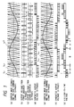
Images


Classifications
-
- H—ELECTRICITY
- H02—GENERATION; CONVERSION OR DISTRIBUTION OF ELECTRIC POWER
- H02M—APPARATUS FOR CONVERSION BETWEEN AC AND AC, BETWEEN AC AND DC, OR BETWEEN DC AND DC, AND FOR USE WITH MAINS OR SIMILAR POWER SUPPLY SYSTEMS; CONVERSION OF DC OR AC INPUT POWER INTO SURGE OUTPUT POWER; CONTROL OR REGULATION THEREOF
- H02M7/00—Conversion of ac power input into dc power output; Conversion of dc power input into ac power output
- H02M7/42—Conversion of dc power input into ac power output without possibility of reversal
- H02M7/44—Conversion of dc power input into ac power output without possibility of reversal by static converters
- H02M7/48—Conversion of dc power input into ac power output without possibility of reversal by static converters using discharge tubes with control electrode or semiconductor devices with control electrode
- H02M7/483—Converters with outputs that each can have more than two voltages levels
- H02M7/49—Combination of the output voltage waveforms of a plurality of converters
Definitions
- the present invention relates to an inverter system for use in a variable-speed AC motor control system, an uninterruptible ac electric power supply and the like, and more particularly it relates to a multiple inverter system having voltage source PWM inverters connected in parallel and performing pulse-width modulation control on its output voltage. It also relates to a control method for the system.
- a parallel and multiple connection of voltage source PWM inverters is already known and has contributed to the down-sizing in capacity of a unit inverter and to the harmonic reduction thereof thereby ensuring reduction of distortion in the output voltage even at a lower switching frequency.
- a PWM control method useful for controlling the inverter output voltage there is known such a prior art as set forth in the Japanese Patent Application Laid-open No.60-98875/1985.
- a phase angle of respective carrier waves for controlling a respective inverter is adapted to become negative-phase from each other with a phase shift of 180 degrees, and the respective inverter is controlled of its output voltage with a PWM signal to be obtained as a result of comparison between these respective carrier waves and a voltage command signal.
- the pulse phases in the synthetic output voltages can be adjusted to become almost the same throughout the whole phases. Therefore, it is possible to minimize distortion in the output voltage of the multiple inverter system, and in particular, to eliminate the harmonic component which is two times the carrier frequency without increasing switching frequency in the inverter system.
- the loss occurring in the inverter system and the load such as motors are ensured to be minimized, thereby contributing to improvement in efficiency and down-sizing of the inverter system and the like. Further, thusly reduced distortion in the output voltage advantageously reduces noise and vibration.
- the main object of the present invention is to reduce harmonics in the output voltage from the parallel-connection multiple inverter without increasing the number of a switching frequency.
- the object of the invention is at least in part accomplished by utilizing a parallel-connection multiple inverter system having: at least two inverter units for converting a DC voltage to an AC voltage, and generating a synthetic output voltage to be output by synthesizing AC voltages from said at least two inverter units; controlling output voltages from the above-mentioned at least two inverter units in response to a pulse width modulation signal to be obtained as a result of comparison between an AC voltage command which serves as a reference value for an output voltage of a respective line phase and two carrier waves which have a phase difference of 180 degrees each other, further in conjunction with a control method for controlling a parallel-connection multiple inverter whereby every time the polarity of said AC voltage command in respective line phases changes, more specifically at every 180 degrees of phase, the phase angle of a respective carrier wave in the corresponding line phase is caused to change.
- This phase angle change in the carrier waves is advantageously effected to be performed such that, in particular, when the polarity of said AC voltage command is in the same polarity with that of an associated AC voltage command in a corresponding relative phase, the corresponding phase angle of the carrier waves in the corresponding line phases are adapted to become in-phase or in negative-phase one another, and further when the respective polarity of said AC voltage commands in the corresponding line phases is in the opposite polarity from each other, the corresponding phase angle of the carrier waves in said corresponding respective line phases is changed to have a phase difference of appraximately 90 degrees.
- a parallel-connection multiple inverter system having: two inverter units each for converting a DC voltage into an AC voltage; a means for synthesizing AC voltages from said respective inverter units to obtain an output voltage; a means for generating a respective voltage command signal serving as a reference value for said output voltage of individual line phase; a means for generating a first carrier wave signal with a predetermined cycle; a means for generating a pulse width modulation signal for an individual line phase in response to said first carrier wave signal and said respective voltage command signal for said individual line phase; a first control means for controlling an output voltage from said first inverter unit responsive to said pulse width modulation signal; a means for generating a second carrier wave having a negative-phase relative to that of said first carrier wave signal; a means for outputting a pulse width modulation signal for an individual line phase in response to said second carrier wave signal and said voltage command signal for said individual line phase; and a second
- FIG. 2 is a schematic block diagram illustrating a main circuit configuration of a parallel-connection multiple inverter according to the invention.
- Fig. 2 shows a parallel-connection arrangement of a first three-phase inverter 1 including switching elements GUP1, GUN1, GVP1, GVN1, GWP1, GWN1, and a second three-phase inverter 2 including switching elements GUP2, GUN2, GVP2, GVN2, GWP2, GWN2, in which an input side of a respective inverter is connected to a DC voltage source in common-use, and output terminals of the respective inverters of the same phase are interconnected in an interphase reactor 3 respectively for respective line phases.
- An output terminal connected to a respective center tap of the respective interphase reactor 3 supplies synthetic voltages obtained to an electric motor 4.
- Figure 3 shows a schematic block diagram illustrating a control circuit of the above-mentioned parallel-connection multiple inverter system embodying the invention.
- numerals 5 denotes a voltage command generator for generating voltage command signals Vu* to Vw* for respective U, V, and W phases.
- 91 to 93 denote a polarity detector for detecting polarity of a respective voltage command signal of a respective line phase then outputting voltage command polarity signals Pu to Pw in accordance.
- 61 to 63 denote a triangular pulse generator for generating a pulse width modulation carrier wave for respective line phases, the triangular pulse generator being provided with a function to change the phase angle of carrier waves in accordance with the change in the voltage command polarity signals Pu through Pw.
- Output signals fcu1, fcv1, fcw1 from triangular pulse generators 61 through 63 are defined respectively as a first carrier signal for a corresponding line phase, and their reversed signals fcu2, fcv2, fcw2 are defined respectively as a second carrier signal for the corresponding line phase.
- 71 through 76 denote comparators for comparing between the voltage command signal of a respective line phase and the associated first and second carrier wave signals thereof thereby to output a pulse width modulation signal therefrom.
- 81P through 86P, and 81N through 86N are gate amplifiers for amplifying the thusly obtained pulse width modulation signals to be converted into drive signals for driving respective switching elements in the first and the second inverters.
- a major difference in the above-mentioned control circuit of the invention distinct from the prior art resides in a novel method for generating a carrier wave as an output signal from the triangular pulse generators 61 through 63.
- the carrier waves in the prior art are all in-phase for respective line phases independent of the polarity of the voltage command signal thereof.
- a phase angle of a respective carrier wave of a respective line phase according to the invention is adapted to change in accordance with the change in the polarity of a voltage command signal of the respective line phase.
- FIG. 4 is a schematic diagram illustrating operation of the triangular wave generator 61.
- the other triangular wave generators 62, 63 are assumed also to operate likewise.
- (a) denotes a U-phase voltage command signal Vu*
- (b) a voltage command polarity signal Pu which is an output from the polarity detector 91
- (c) a reference clock signal Ck
- (d) a first carrier wave signal fcu1 which is an output from the triangular wave generator 61, respectively.
- the polarity detector 91 enters a U-phase voltage command signal Vu* to be converted into a voltage command polarity signal Pu indicative of the change in the polarity thereof.
- the triangular pulse generator 61 outputs a carrier wave signal fcu1, of a triangular wave having a maximum or a minimum peak for every two pulses of the reference clock signal Ck when the voltage command polarity signal Pu is constant, whereas, when the voltage command polarity signal Pu changes, it outputs a carrier wave signal fcu1 in which during a half cycle between a peak-to-peak interval immediately following the occurrence of a polarity change, a triangular pulse is generated such that its peak coincides with one pulse interval of the reference clock signal Ck instead of two pulses at normal coincidence.
- the cycle period of the carrier wave signal fcu1 immediately following the event of the polarity change is multiplied by 0.5 only during a half period thereof.
- the carrier wave signal fcu1 after the polarity change in the voltage command signal Vu* as shown in a solid line is caused to advance 90 degrees in phase in comparison with triangular waves indicated in dotted lines assuming no polarity change.
- Fig. 1 shows exemplary operational waveforms in a multiple inverter system utilizing a control circuit of Fig. 3 embodying the invention.
- Fig.1 (a) illustrates the first and the second carrier wave signals fcu1, fcu2 and the voltage command signal Vu* each on the U-phase. It can be understood from this illustration that immediately after the polarity of the voltage command signal changes from positive to negative or vice versa, a particular cycle of the respective carrier wave signal, more particularly, during its half cycle immediately thereafter becomes 0.5 times of the normal, thereby effecting a phase angle change to take place in the carrier wave signal.
- (b) illustrates a U-phase output voltage from the first inverter, obtained through pulse width modulation in comparison with the first carrier wave signal and the U-phase voltage command signal.
- (c) illustrates a U-phase output voltage from the second inverter, obtained through pulse width modulation in comparison with the second carrier wave signal and the U-phase voltage command signal.
- (d) shows a U-phase synthetic output voltage obtained as an average of the first and the second output voltages.
- (e) shows a first and a second carrier wave signals fcv1, fcv2, and a voltage command signal Vv* on a V-phase.
- Fig. 5 a likewise operational waveform diagram as shown in Fig.1 is given in Fig. 5 indicative of the prior art.
- Fig.5 shows a first and a second carrier wave signals fc1, fc2, and voltage command signals Vu*, Vv*, Vw* for respective line phases of U, V, and W.
- the first and the second carrier wave signals are common to respective voltage command signals of respective line phases. Any phase angle of the carrier waves is not caused to change in accordance with the change in polarity of the voltage command as has been changed and indicated in the solid line in Fig.4, but holds on a constant cycle as shown in dotted lines therein.
- (b) is a U-phase output voltage from the first inverter obtained through pulse width modulation by comparison between the first carrier wave signal and the U-phase voltage command signal.
- (c) is a U-phase output voltage from the second inverter obtained through pulse width modulation by comparison between the second carrier wave signal and the U-phase voltage command signal.
- (d) is a U-phase synthetic output voltage obtained as an average of the first and the second output voltages.
- (e) is a V-phase synthetic output voltage obtained likewise.
- (f) is a U-V line-to-line voltage waveform obtained as a difference between (d) and (e).
- the pulse phase of the U-phase synthetic output voltage and the pulse phase of the V-phase synthetic output voltage having an opposite polarity relationship
- the pulse components in the respective pulse phases are amplified twice as great in the U-V line-toline voltage.
- the pulse frequencies of the U-phase synthetic output voltage and the V-phase synthetic output voltage equal twice the carrier wave frequency, there occurs particularly a large harmonic as great as twice the carrier wave frequency in the line-to-line voltage.
- the phase angle of one of the corresponding carrier waves may be effected either to advance or lag 90 degrees from the other.
- the phase angle of the carrier wave was advanced 90 degrees so that the pulse phase was effected to change 180 degrees.
- Figure 7 shows another operational waveform output from a triangular wave generator where the phase angle of the carrier wave is lagged 90 degrees to the same effect as above.
- (a) denotes a voltage command signal
- (b) a voltage command polarity signal output from a polarity detector
- (c) a reference clock signal
- (d) a carrier wave signal output from the triangular wave generator.
- a voltage command polarity signal from a polarity detector 91 is entered into a triangular pulse generator 61A from which is output a carrier wave signal in a triangular waveform having a maximum or minimum peak thereof for every two pulses of the reference clock signal when the voltage command polarity signal is constant, whereas when the voltage command polarity signal undergoes a change, a carrier wave signal is output in a triangular waveform having a pulse width equal to 3 pulse intervals of the reference clock signal only during a half cycle to be defined between a peak-to-peak cycle thereof immediately following the polarity change in the voltage command polarity signal.
- the carrier wave signal immediately after the occurrence of polarity change in the voltage command signal is caused to change its cycle period by being multiplied by 1.5 only during a half cycle thereof, thereby the carrier wave signal after the occurrence of the polarity change in the voltage command signal is effected to lag 90 degrees in phase than triangular waveforms shown in dotted lines in which no polarity change is assumed to have occurred.
- FIG. 8 there is shown an operational waveform diagram of a parallel-connection multiple inverter system of a second preferred embodiment of the invention.
- Signals of (a) through (g) are the same as in Fig.1.
- the pulse phase of a first and a second carrier wave signals during a half period thereof is multiplied by 1.5, thus causing a phase angle shift in the carrier wave signal in accordance.
- the changing in phase in the first and the second carrier waves is effected to take place by means of the polarity detection signal, but not limited thereto, it should be construed that the same effect can be accomplished by means of a phase angle detection signal indicative of a particular phase of the voltage command signal as well.
- the interphase reactor by way of example is utilized to constitute the main circuit configuration of the parallel-connection multiple inverter system of the invention so as to synthesize AC voltages supplied from two inverter units to obtain an output voltage. It is not limited thereto, but it should be construed that the same effect of the invention can be obtained by utilizing a transformer means for interconnecting multiple inverters.
Abstract
Description
- The present invention relates to an inverter system for use in a variable-speed AC motor control system, an uninterruptible ac electric power supply and the like, and more particularly it relates to a multiple inverter system having voltage source PWM inverters connected in parallel and performing pulse-width modulation control on its output voltage. It also relates to a control method for the system.
- A parallel and multiple connection of voltage source PWM inverters is already known and has contributed to the down-sizing in capacity of a unit inverter and to the harmonic reduction thereof thereby ensuring reduction of distortion in the output voltage even at a lower switching frequency. As a PWM control method useful for controlling the inverter output voltage, there is known such a prior art as set forth in the Japanese Patent Application Laid-open No.60-98875/1985. Namely, in a multiple-connection inverter system including an interphase reactor provided between respective corresponding output terminals of two inverter units, a phase angle of respective carrier waves for controlling a respective inverter is adapted to become negative-phase from each other with a phase shift of 180 degrees, and the respective inverter is controlled of its output voltage with a PWM signal to be obtained as a result of comparison between these respective carrier waves and a voltage command signal.
- Through such arrangements, since an output current to be obtained from the center tap of the interphase reactor becomes approximately twice as large as a current of each respective inverter, it becomes possible to drive an AC motor having a capacity twice as large as a unit capacity of each inverter. Further, by adding a different control signal to the first inverter and the second inverter respectively, it becomes possible to reduce a waveform distortion such as harmonics in a synthetic voltage in comparison with that of a single inverter.
- In the parallel-connection multiple inverter system according to the invention, by ensuring the phase angle of the carrier wave signals to change in accordance with the change in polarity of the voltage command signal of the individual line phase, the pulse phases in the synthetic output voltages can be adjusted to become almost the same throughout the whole phases. Thereby, it is possible to minimize distortion in the output voltage of the multiple inverter system, and in particular, to eliminate the harmonic component which is two times the carrier frequency without increasing switching frequency in the inverter system.
- Thereby, the following advantageous effects according to the invention may be realized. The loss occurring in the inverter system and the load such as motors are ensured to be minimized, thereby contributing to improvement in efficiency and down-sizing of the inverter system and the like. Further, thusly reduced distortion in the output voltage advantageously reduces noise and vibration.
- The above-mentioned prior art, however, involved such a problem due to a cause to be described later that in the synthetic output voltage obtained by synthesizing outputs from respective inverters, a harmonic component in double frequency of a carrier wave becomes particularly large. Some countermeasures such as to increase the number of frequency of the carrier wave or the like may be contemplated to be taken in order to reduce an amplitude of this harmonic component relative to a fundamental wave, which, however, results in another problem that the switching loss in the inverter increases thereby lowering its conversion efficiency.
- The main object of the present invention is to reduce harmonics in the output voltage from the parallel-connection multiple inverter without increasing the number of a switching frequency.
- The object of the invention is at least in part accomplished by utilizing a parallel-connection multiple inverter system having: at least two inverter units for converting a DC voltage to an AC voltage, and generating a synthetic output voltage to be output by synthesizing AC voltages from said at least two inverter units; controlling output voltages from the above-mentioned at least two inverter units in response to a pulse width modulation signal to be obtained as a result of comparison between an AC voltage command which serves as a reference value for an output voltage of a respective line phase and two carrier waves which have a phase difference of 180 degrees each other, further in conjunction with a control method for controlling a parallel-connection multiple inverter whereby every time the polarity of said AC voltage command in respective line phases changes, more specifically at every 180 degrees of phase, the phase angle of a respective carrier wave in the corresponding line phase is caused to change. This phase angle change in the carrier waves is advantageously effected to be performed such that, in particular, when the polarity of said AC voltage command is in the same polarity with that of an associated AC voltage command in a corresponding relative phase, the corresponding phase angle of the carrier waves in the corresponding line phases are adapted to become in-phase or in negative-phase one another, and further when the respective polarity of said AC voltage commands in the corresponding line phases is in the opposite polarity from each other, the corresponding phase angle of the carrier waves in said corresponding respective line phases is changed to have a phase difference of appraximately 90 degrees.
- Further, the above-mentioned main object of the invention is at least in part accomplished by providing: a parallel-connection multiple inverter system having: two inverter units each for converting a DC voltage into an AC voltage; a means for synthesizing AC voltages from said respective inverter units to obtain an output voltage; a means for generating a respective voltage command signal serving as a reference value for said output voltage of individual line phase; a means for generating a first carrier wave signal with a predetermined cycle; a means for generating a pulse width modulation signal for an individual line phase in response to said first carrier wave signal and said respective voltage command signal for said individual line phase; a first control means for controlling an output voltage from said first inverter unit responsive to said pulse width modulation signal; a means for generating a second carrier wave having a negative-phase relative to that of said first carrier wave signal; a means for outputting a pulse width modulation signal for an individual line phase in response to said second carrier wave signal and said voltage command signal for said individual line phase; and a second control means for controlling an output voltage from said second inverter unit responsive to said pulse width modulation signal, wherein the parallel-connection multiple inverter system is characterized by comprising: a polarity detection means for detecting a polarity of said AC voltage command of said individual line phase; and a means for variably changing the phase angle or frequency of said first and second carrier waves for individual line phases in response to a polarity detection value from said polarity detection means.
- When observing an output voltage from a parallel-connection multiple inverter system in views of respective line phases, in a particular region where, for example, both a U-phase voltage command and a V-phase voltage command are either in a positive polarity or negative polarity, since pulse phases of a U-phase synthetic output voltage and a V-phase synthetic output voltage have an in-phase relationship likewise in the prior art, pulse components are cancelled out in a resultant U-V line-toline voltage.
- Further, in a region where an opposite polarity is caused to occur between two phase voltage commands such that a U-phase voltage command is of positive polarity while a V-phase voltage command is of negative polarity, by changing the phase angle of a carrier wave by 90 degrees in a respective line phase in accordance with the polarity of an AC voltage command in the respective line phase, the pulse phase of a synthetic output voltage is effected to change 180 degrees, thus ensuring a pulse phase relationship between the respective synthetic output voltages to become in-phase in this opposite polarity region, thus cancelling out pulse components therebetween. Thereby, it is possible according to the invention to reduce the harmonic component of the line-to-line voltage which is two times the carrier frequency.
- Incidently, since the pulse phase relationship between the U-phase synthetic output voltage and the V-phase synthetic output voltage becomes negative-phase according to the prior art, a pulse component in a U-V line-to-line voltage is amplified twice as large. Since a pulse frequency of the U-phase synthetic output voltage and the V-phase synthetic output voltage equals a two-fold of the carrier frequency, it occurs that the harmonic component of the line-to-line voltage which is two times the carrier frequency becomes particularly large.
- These and other objects, aspects and embodiments of the present invention will be described in more detail with reference to the accompanying drawings, in which:
- Fig.1 is an operational waveform diagram of an inverter of one embodiment of the invention;
- Fig.2 is a main circuit configuration of the inverter of one embodiment of the invention;
- Fig.3 is a control circuit block diagram of the inverter of one embodiment of the invention;
- Fig.4 is an operational waveform of a triangular pulse generator according to the invention;
- Fig.5 is an operational waveform diagram indicative of operation of an prior art parallel-connection multiple inverter;
- Fig.6 compares harmonic amplitudes in line-to-line voltages between the present invention and the prior art;
- Fig.7 is an operational waveform indicative of operation of a triangular pulse generator of a second embodiment of the invention; and
- Fig.8 is an operational waveform diagram indicative of operation of an inverter of the second embodiment of the invention.
- With reference to Figure 2, a one preferred embodiment of the invention will be set forth in the following.
- Figure 2 is a schematic block diagram illustrating a main circuit configuration of a parallel-connection multiple inverter according to the invention. Fig. 2 shows a parallel-connection arrangement of a first three-
phase inverter 1 including switching elements GUP1, GUN1, GVP1, GVN1, GWP1, GWN1, and a second three-phase inverter 2 including switching elements GUP2, GUN2, GVP2, GVN2, GWP2, GWN2, in which an input side of a respective inverter is connected to a DC voltage source in common-use, and output terminals of the respective inverters of the same phase are interconnected in aninterphase reactor 3 respectively for respective line phases. An output terminal connected to a respective center tap of therespective interphase reactor 3 supplies synthetic voltages obtained to anelectric motor 4. - Figure 3 shows a schematic block diagram illustrating a control circuit of the above-mentioned parallel-connection multiple inverter system embodying the invention. In reference to Fig.3,
numerals 5 denotes a voltage command generator for generating voltage command signals Vu* to Vw* for respective U, V, and W phases. 91 to 93 denote a polarity detector for detecting polarity of a respective voltage command signal of a respective line phase then outputting voltage command polarity signals Pu to Pw in accordance. 61 to 63 denote a triangular pulse generator for generating a pulse width modulation carrier wave for respective line phases, the triangular pulse generator being provided with a function to change the phase angle of carrier waves in accordance with the change in the voltage command polarity signals Pu through Pw. Output signals fcu₁, fcv₁, fcw₁ fromtriangular pulse generators 61 through 63 are defined respectively as a first carrier signal for a corresponding line phase, and their reversed signals fcu₂, fcv₂, fcw₂ are defined respectively as a second carrier signal for the corresponding line phase. 71 through 76 denote comparators for comparing between the voltage command signal of a respective line phase and the associated first and second carrier wave signals thereof thereby to output a pulse width modulation signal therefrom. 81P through 86P, and 81N through 86N are gate amplifiers for amplifying the thusly obtained pulse width modulation signals to be converted into drive signals for driving respective switching elements in the first and the second inverters. - A major difference in the above-mentioned control circuit of the invention distinct from the prior art resides in a novel method for generating a carrier wave as an output signal from the
triangular pulse generators 61 through 63. Namely, the carrier waves in the prior art are all in-phase for respective line phases independent of the polarity of the voltage command signal thereof. In contrast, a phase angle of a respective carrier wave of a respective line phase according to the invention is adapted to change in accordance with the change in the polarity of a voltage command signal of the respective line phase. - Figure 4 is a schematic diagram illustrating operation of the
triangular wave generator 61. The othertriangular wave generators polarity detector 91, (c) a reference clock signal Ck, and (d) a first carrier wave signal fcu₁ which is an output from thetriangular wave generator 61, respectively. Thepolarity detector 91 enters a U-phase voltage command signal Vu* to be converted into a voltage command polarity signal Pu indicative of the change in the polarity thereof. Thetriangular pulse generator 61 outputs a carrier wave signal fcu₁, of a triangular wave having a maximum or a minimum peak for every two pulses of the reference clock signal Ck when the voltage command polarity signal Pu is constant, whereas, when the voltage command polarity signal Pu changes, it outputs a carrier wave signal fcu₁ in which during a half cycle between a peak-to-peak interval immediately following the occurrence of a polarity change, a triangular pulse is generated such that its peak coincides with one pulse interval of the reference clock signal Ck instead of two pulses at normal coincidence. As a results, the cycle period of the carrier wave signal fcu₁ immediately following the event of the polarity change is multiplied by 0.5 only during a half period thereof. Thereby, the carrier wave signal fcu₁ after the polarity change in the voltage command signal Vu* as shown in a solid line is caused to advance 90 degrees in phase in comparison with triangular waves indicated in dotted lines assuming no polarity change. - Fig. 1 shows exemplary operational waveforms in a multiple inverter system utilizing a control circuit of Fig. 3 embodying the invention. In Fig.1, (a) illustrates the first and the second carrier wave signals fcu₁, fcu₂ and the voltage command signal Vu* each on the U-phase. It can be understood from this illustration that immediately after the polarity of the voltage command signal changes from positive to negative or vice versa, a particular cycle of the respective carrier wave signal, more particularly, during its half cycle immediately thereafter becomes 0.5 times of the normal, thereby effecting a phase angle change to take place in the carrier wave signal. In the likewise drawing, (b) illustrates a U-phase output voltage from the first inverter, obtained through pulse width modulation in comparison with the first carrier wave signal and the U-phase voltage command signal. Likewise, (c) illustrates a U-phase output voltage from the second inverter, obtained through pulse width modulation in comparison with the second carrier wave signal and the U-phase voltage command signal. (d) shows a U-phase synthetic output voltage obtained as an average of the first and the second output voltages. (e) shows a first and a second carrier wave signals fcv₁, fcv₂, and a voltage command signal Vv* on a V-phase. It can be understood, likewise the U-phase, that during a half cycle of the carrier wave signal immediately following the change of the polarity of the voltage command signal from positive to negative or vice versa, the cycle period thereof is multiplied by 0.5, thereby causing a phase angle change to take place in the carrier wave signal. (f) shows a V-phase synthetic output voltage obtained likewise (d). (g) shows a waveform of a U-V line-to-line voltage obtained as a difference between (d) and (f).
- In order to compare the advantages and effects of the present invention over the prior art, a likewise operational waveform diagram as shown in Fig.1 is given in Fig. 5 indicative of the prior art. In Fig.5, (a) shows a first and a second carrier wave signals fc₁, fc₂, and voltage command signals Vu*, Vv*, Vw* for respective line phases of U, V, and W. The first and the second carrier wave signals are common to respective voltage command signals of respective line phases. Any phase angle of the carrier waves is not caused to change in accordance with the change in polarity of the voltage command as has been changed and indicated in the solid line in Fig.4, but holds on a constant cycle as shown in dotted lines therein. (b) is a U-phase output voltage from the first inverter obtained through pulse width modulation by comparison between the first carrier wave signal and the U-phase voltage command signal. (c) is a U-phase output voltage from the second inverter obtained through pulse width modulation by comparison between the second carrier wave signal and the U-phase voltage command signal. (d) is a U-phase synthetic output voltage obtained as an average of the first and the second output voltages. (e) is a V-phase synthetic output voltage obtained likewise. (f) is a U-V line-to-line voltage waveform obtained as a difference between (d) and (e).
- In comparison of the operational waveforms in Fig.1 and Fig.5, we can note a significant difference in each of the line-to-line voltage waveforms. First, with reference to Fig.5 indicative of the prior art, since the same carrier wave signals are used in common for a respective line phase, when the U-phase voltage command and the V-phase voltage command are both positive polarity or negative polarity as shown in a region indicated by A, the pulse phase of the U-phase synthetic output voltage and the pulse phase of the V-phase synthetic output voltage having an in-phase relationship, pulse components in the respective pulse phase are effected to be cancelled out in a resultant U-V line-to-line voltage. However, when the U-phase voltage command is positive polarity and the V-phase voltage command is negative polarity as shown in a region indicated by B, the pulse phase of the U-phase synthetic output voltage and the pulse phase of the V-phase synthetic output voltage having an opposite polarity relationship, the pulse components in the respective pulse phases are amplified twice as great in the U-V line-toline voltage. Further, since the pulse frequencies of the U-phase synthetic output voltage and the V-phase synthetic output voltage equal twice the carrier wave frequency, there occurs particularly a large harmonic as great as twice the carrier wave frequency in the line-to-line voltage.
- Next, with reference to Fig.1 illustrative of the present invention, in a region as indicated by A where both the U-phase voltage command and the V-phase voltage command are either in a positive polarity or negative polarity, since corresponding phase angles of the respective carrier wave signal of the U-phase and the V-phase become in-phase each other likewise in Fig.5 indicative of the prior art except for a half cycle immediately following the occurrence of a polarity change in the voltage command, and thereby since the pulse phases of the U-phase synthetic output voltage and the V-phase synthetic output voltage have an in-phase relationship, the resultant pulse components are cancelled out in the U-V line-to-line voltage. Further, also in a region as indicated by B where the U-phase voltage command is, for example, positive polarity and the V-phase voltage command is negative polarity, since a phase angle change of 90 degrees caused in a carrier wave in the respective line phase undergoing a polarity change will result in a pulse phase change of 180 degrees in its synthetic output voltage, thereby a pulse phase relationship between the corresponding synthetic output voltages even in this region being advantageously effected to become in-phase, the resultant pulse components are cancelled out. Thereby, the harmonic component of the line-to-line voltage which is two times the carrier frequency can be cancelled out. The advantageous effect of the invention over the prior art is obvious from the comparison of the operational waveforms at the line-to-line voltages, where the U-V line-to-line voltage obtained according to the invention consists of only a voltage pulse having a level approximately equal to an average voltage indicated in dotted lines, and thus having a reduced voltage distortion.
- Further, with reference to Fig.1, although it has been described that in the region indicated by A where both the U-phase voltage command and the V-phase voltage command are either positive polarity or negative polarity, the respective phase angles of the corresponding carrier waves of the respective line phases are assumed to be in-phase, but not limited thereto, it should be construed that they may be in an opposite polarity as well. It is because that the phase angles of the synthetic output voltages of respective line phases are simply shifted 180 degrees as a whole, and which causes no change in the in-phase relationship between the pulse phases of the synthetic output voltages of respective line phases.
- With reference to Figure 6, there are compared harmonic amplitudes of the line-to-line voltage between (a) indicative of one embodiment of the invention and (b) indicative of the prior art. In Fig.6, f₀ denotes the frequency of a voltage command signal, and fc denotes the frequency of a carrier wave. By applying the present invention, such a component of those harmonics of the line-to-line voltage, in particular, as a component 2fc±f₀ present in the vicinity of a double frequency of the carrier frequency is effected to be reduced remarkably, thereby minimizing the voltage distortion.
- The principle of the present invention will be set forth in brief as follows. In view of the problems associated with the prior art that when the polarities of the voltage commands of corresponding respective line phases become opposite as observed between line-to-line as indicated by the B region in Fig.5, the pulse phases of the synthetic output voltages of respective line phases become opposite polarity as shown by (d) and (e), thereby the double frequency component twice the carrier frequency becomes very large in the line-to-line voltage, the present invention is contemplated to sufficiently reduce the harmonic component of the line-to-line voltage which is two times the carrier frequency through the steps of changing either one of the corresponding pulse phases by 180 degrees such that both the pulse phases of synthetic output voltages of respective line phases are always kept in-phase.
- Hence, in order to cause a pulse phase change of 180 degrees in one of the synthetic output voltage, the pulse frequency of the synthetic output voltages being two times the carrier frequency, it will be readily understood that the phase angle of one of the corresponding carrier waves may be effected either to advance or lag 90 degrees from the other. In the first embodiment of the invention, the phase angle of the carrier wave was advanced 90 degrees so that the pulse phase was effected to change 180 degrees.
- By contrast, Figure 7 shows another operational waveform output from a triangular wave generator where the phase angle of the carrier wave is lagged 90 degrees to the same effect as above. In Figure 7, (a) denotes a voltage command signal, (b) a voltage command polarity signal output from a polarity detector, (c) a reference clock signal, and (d) a carrier wave signal output from the triangular wave generator.
- The operation of this exemplary case of the invention will be described below. A voltage command polarity signal from a
polarity detector 91 is entered into a triangular pulse generator 61A from which is output a carrier wave signal in a triangular waveform having a maximum or minimum peak thereof for every two pulses of the reference clock signal when the voltage command polarity signal is constant, whereas when the voltage command polarity signal undergoes a change, a carrier wave signal is output in a triangular waveform having a pulse width equal to 3 pulse intervals of the reference clock signal only during a half cycle to be defined between a peak-to-peak cycle thereof immediately following the polarity change in the voltage command polarity signal. Consequently, the carrier wave signal immediately after the occurrence of polarity change in the voltage command signal is caused to change its cycle period by being multiplied by 1.5 only during a half cycle thereof, thereby the carrier wave signal after the occurrence of the polarity change in the voltage command signal is effected to lag 90 degrees in phase than triangular waveforms shown in dotted lines in which no polarity change is assumed to have occurred. - With reference to Figure 8, there is shown an operational waveform diagram of a parallel-connection multiple inverter system of a second preferred embodiment of the invention. Signals of (a) through (g) are the same as in Fig.1. In particular, as can be recognized both in (a) and (e), immediately after the polarity of a voltage command signal in a respective line phase changes from positive polarity to negative polarity and vice versa, the pulse phase of a first and a second carrier wave signals during a half period thereof is multiplied by 1.5, thus causing a phase angle shift in the carrier wave signal in accordance. Thereby, in a region where a U-phase voltage command is positive polarity and a V-phase voltage command is negative polarity, namely when both voltage commands are in an opposite polarity relationship, since a phase angle lag of 90 degrees caused in the carrier wave on a respective line phase undergoing a polarity change will result in a pulse phase change of 180 degrees in the synthetic output voltage, thereby ensuring an in-phase pulse phase relationship to be realized between respective synthetic output voltages even in this region, resultant harmonic pulse components are effectively cancelled out therebetween. Thereby, according to this second embodiment of the invention likewise in the aforementioned first embodiment of the invention, the harmonic component of the line-to-line voltage which is two times the carrier frequency can be advantageously reduced as well.
- In the preferred embodiments of the invention described heretofore, the changing in phase in the first and the second carrier waves is effected to take place by means of the polarity detection signal, but not limited thereto, it should be construed that the same effect can be accomplished by means of a phase angle detection signal indicative of a particular phase of the voltage command signal as well.
- Further, in the foregoing preferred embodiments of the invention, the interphase reactor by way of example is utilized to constitute the main circuit configuration of the parallel-connection multiple inverter system of the invention so as to synthesize AC voltages supplied from two inverter units to obtain an output voltage. It is not limited thereto, but it should be construed that the same effect of the invention can be obtained by utilizing a transformer means for interconnecting multiple inverters.
- Still further, as an exemplary object for applying the control method according to the invention we have dealt with the inverters which convert a direct current into an alternating current to supply an electric power to a load, but it is not limited thereto, and it should be understood that the advantage and effect of the invention can be applied to a line-side converter which converts an alternating current into a direct current.
- Moreover, in the description heretofore, for easier understanding and simplification of description, the arrangement and operation of the pulse width modulation circuit have been described by way of example of the analog circuits and analog waveforms, but not limited thereto, it should be construed that the same effect and advantage of the invention can be accomplished by employing a microprocessor or the like so as to digitalize information and operate on a pertinent software.
Claims (6)
- A control method for controlling a parallel-connection multiple inverter system comprising at least two inverter units for converting a direct current(DC) voltage into an alternating current(AC) voltage, said parallel-connection multiple inverter system being adapted to output a synthetic output voltage by synthesizing AC voltages from respective inverter units,
wherein said control method controls a respective output voltage from the at least two inverter units on the basis of a pulse width modulation (PWM) signal to be obtained from comparison between an AC voltage command serving as a reference value for an output voltage of an individual line phase and two carrier waves of the individual line phase, said carrier waves having a phase difference of 180 degrees from each other, and wherein
a respective phase angle of carrier waves in a corresponding individual line phase is characterized by being changed, every time a polarity of said AC voltage command of said individual line phase is caused to change (at every 180 degrees of cyclic period), relative to a preceding phase angle of the carrier waves prior to the occurrence of the change in polarity of said AC voltage command. - A control method for controlling a parallel-connection multiple inverter system according to claim 1 wherein
a respective phase angle of carrier waves in the corresponding individual line phase is characterized by being adapted to become either in-phase or negative-phase relative to that of carrier waves in the other one of the corresponding individual line phase when polarity of said AC voltage commands of corresponding line phases is in the same polarity, and further to have a phase difference of approximately 90 degrees between said corresponding carrier waves between said corresponding individual line phases when polarity of said AC voltage commands of corresponding line phases is in opposite polarity. - A parallel-connection multiple inverter system having: two inverter units each for converting a DC voltage into an AC voltage; a means for synthesizing AC voltages from said respective inverter units to obtain an output voltage; a means for generating a respective voltage command signal serving as a reference value for said output voltage of individual line phase; a means for generating a first carrier wave signal with a predetermined cycle; a means for generating a pulse width modulation signal for an individual line phase in response to said first carrier wave signal and said respective voltage command signal for said individual line phase; a first control means for controlling an output voltage from said first inverter unit responsive to said pulse width modulation signal; a means for generating a second carrier wave having a negative-phase relative to that of said first carrier wave signal; a means for outputting a pulse width modulation signal for an individual line phase in response to said second carrier wave signal and said voltage command signal for said individual line phase; and a second control means for controlling an output voltage from said second inverter unit responsive to said pulse width modulation signal, wherein
the parallel-connection multiple inverter system is characterized by comprising: a polarity detection means for detecting a polarity of said AC voltage command of said individual line phase; and a means for variably changing the phase angle or frequency of said first and second carrier waves for individual line phases in response to a polarity detection value from said polarity detection means. - A parallel-connection multiple inverter system according to claim 3 wherein at the time when said voltage command changes its polarity, a corresponding respective phase angle of said first and second carrier waves in corresponding line phases is characterized by being adapted either to advance or lag by 90 degrees in cyclic period.
- A parallel-connection multiple inverter system according to claim 3 wherein when said voltage command changes its polarity, a corresponding cycle period of said first and second carrier waves in corresponding individual line phases is characterized by being multiplied either by 0.5 or 1.5 during a half cycle of said corresponding carrier waves.
- A variable speed AC drive system wherein the variable speed AC drive system is characterized by driving an alternating current motor according to one of claims 1 through 5.
Applications Claiming Priority (2)
| Application Number | Priority Date | Filing Date | Title |
|---|---|---|---|
| JP4319705A JP2888068B2 (en) | 1992-11-30 | 1992-11-30 | Control method of parallel multiple inverter and device thereof |
| JP319705/92 | 1992-11-30 |
Publications (3)
| Publication Number | Publication Date |
|---|---|
| EP0600635A2 true EP0600635A2 (en) | 1994-06-08 |
| EP0600635A3 EP0600635A3 (en) | 1994-09-07 |
| EP0600635B1 EP0600635B1 (en) | 1997-05-14 |
Family
ID=18113261
Family Applications (1)
| Application Number | Title | Priority Date | Filing Date |
|---|---|---|---|
| EP19930309161 Expired - Lifetime EP0600635B1 (en) | 1992-11-30 | 1993-11-17 | Parallel-connection multiple inverter system and control method therefor |
Country Status (4)
| Country | Link |
|---|---|
| EP (1) | EP0600635B1 (en) |
| JP (1) | JP2888068B2 (en) |
| DE (1) | DE69310683T2 (en) |
| FI (1) | FI935319A (en) |
Cited By (8)
| Publication number | Priority date | Publication date | Assignee | Title |
|---|---|---|---|---|
| DE10110615A1 (en) * | 2001-03-06 | 2002-09-19 | Bosch Gmbh Robert | Process for generating drive pulses for power semiconductors |
| DE102005060354A1 (en) * | 2005-12-16 | 2007-06-21 | Siemens Ag | Modular inverter system |
| CN103516239A (en) * | 2012-06-29 | 2014-01-15 | 通用电气公司 | Improved modulating system and method for converter |
| CN109546921A (en) * | 2017-09-22 | 2019-03-29 | 法雷奥西门子新能源汽车(德国)有限公司 | The inverter of motor, for motor vehicle motor and the method for operating inverter |
| US10833603B2 (en) | 2017-01-30 | 2020-11-10 | Carrier Corporation | Method of controlling paralleled passive front-end rectifiers with and without inter-leaving |
| US10944335B2 (en) | 2017-01-30 | 2021-03-09 | Carrier Corporation | Paralleled passive front-end rectifiers with and without interleaving |
| CN113595425A (en) * | 2021-09-09 | 2021-11-02 | 上海电动工具研究所(集团)有限公司 | Five-level inverter power supply based on H-bridge cross carrier magnetic coupling control |
| WO2022001943A1 (en) * | 2020-06-29 | 2022-01-06 | 中兴通讯股份有限公司 | Ripple current control method and apparatus, electronic device, and computer-readable storage medium |
Families Citing this family (4)
| Publication number | Priority date | Publication date | Assignee | Title |
|---|---|---|---|---|
| JP4501483B2 (en) * | 2004-03-24 | 2010-07-14 | 株式会社明電舎 | Multiphase series multiple power converter and PWM control method thereof |
| DE102007063434A1 (en) | 2007-06-29 | 2009-01-02 | Enasys Gmbh | Inverter system and control method |
| JP6561663B2 (en) * | 2015-08-03 | 2019-08-21 | 富士電機株式会社 | Power converter |
| JP6961096B2 (en) * | 2018-08-30 | 2021-11-05 | 日立Astemo株式会社 | Inverter device |
Citations (3)
| Publication number | Priority date | Publication date | Assignee | Title |
|---|---|---|---|---|
| JPS6098875A (en) * | 1983-10-31 | 1985-06-01 | Yaskawa Electric Mfg Co Ltd | Controlling method of multiple coupling inverter |
| EP0244186A2 (en) * | 1986-04-29 | 1987-11-04 | David C. Hoffmann | Electronic power supply |
| US5142468A (en) * | 1991-05-16 | 1992-08-25 | General Atomics | Power conditioning system for use with two PWM inverters and at least one other load |
Family Cites Families (1)
| Publication number | Priority date | Publication date | Assignee | Title |
|---|---|---|---|---|
| DE4111733C1 (en) * | 1991-04-08 | 1992-09-17 | Licentia Patent-Verwaltungs-Gmbh, 6000 Frankfurt, De | Universal symmetrising method for current distribution in parallel three=phase inverters - controlling pulse formation w.r.t. shunt or zero current thresholds by supplying corresp. null vectors |
-
1992
- 1992-11-30 JP JP4319705A patent/JP2888068B2/en not_active Expired - Lifetime
-
1993
- 1993-11-17 DE DE1993610683 patent/DE69310683T2/en not_active Expired - Fee Related
- 1993-11-17 EP EP19930309161 patent/EP0600635B1/en not_active Expired - Lifetime
- 1993-11-29 FI FI935319A patent/FI935319A/en not_active Application Discontinuation
Patent Citations (3)
| Publication number | Priority date | Publication date | Assignee | Title |
|---|---|---|---|---|
| JPS6098875A (en) * | 1983-10-31 | 1985-06-01 | Yaskawa Electric Mfg Co Ltd | Controlling method of multiple coupling inverter |
| EP0244186A2 (en) * | 1986-04-29 | 1987-11-04 | David C. Hoffmann | Electronic power supply |
| US5142468A (en) * | 1991-05-16 | 1992-08-25 | General Atomics | Power conditioning system for use with two PWM inverters and at least one other load |
Non-Patent Citations (1)
| Title |
|---|
| PATENT ABSTRACTS OF JAPAN vol. 9, no. 251 (E-348) 8 October 1985 & JP-A-60 098 875 (YASUKAWA DENKI SEISAKUSHO K.K.) 1 June 1985 * |
Cited By (11)
| Publication number | Priority date | Publication date | Assignee | Title |
|---|---|---|---|---|
| DE10110615A1 (en) * | 2001-03-06 | 2002-09-19 | Bosch Gmbh Robert | Process for generating drive pulses for power semiconductors |
| DE102005060354A1 (en) * | 2005-12-16 | 2007-06-21 | Siemens Ag | Modular inverter system |
| CN103516239A (en) * | 2012-06-29 | 2014-01-15 | 通用电气公司 | Improved modulating system and method for converter |
| US10833603B2 (en) | 2017-01-30 | 2020-11-10 | Carrier Corporation | Method of controlling paralleled passive front-end rectifiers with and without inter-leaving |
| US10944335B2 (en) | 2017-01-30 | 2021-03-09 | Carrier Corporation | Paralleled passive front-end rectifiers with and without interleaving |
| CN109546921A (en) * | 2017-09-22 | 2019-03-29 | 法雷奥西门子新能源汽车(德国)有限公司 | The inverter of motor, for motor vehicle motor and the method for operating inverter |
| WO2022001943A1 (en) * | 2020-06-29 | 2022-01-06 | 中兴通讯股份有限公司 | Ripple current control method and apparatus, electronic device, and computer-readable storage medium |
| CN114094803A (en) * | 2020-06-29 | 2022-02-25 | 中兴通讯股份有限公司 | Ripple current control method and apparatus, electronic device, and computer-readable storage medium |
| EP4170885A4 (en) * | 2020-06-29 | 2023-11-29 | ZTE Corporation | Ripple current control method and apparatus, electronic device, and computer-readable storage medium |
| CN114094803B (en) * | 2020-06-29 | 2024-03-12 | 中兴通讯股份有限公司 | Ripple current control method and apparatus, electronic device, and computer-readable storage medium |
| CN113595425A (en) * | 2021-09-09 | 2021-11-02 | 上海电动工具研究所(集团)有限公司 | Five-level inverter power supply based on H-bridge cross carrier magnetic coupling control |
Also Published As
| Publication number | Publication date |
|---|---|
| DE69310683D1 (en) | 1997-06-19 |
| EP0600635A3 (en) | 1994-09-07 |
| FI935319A0 (en) | 1993-11-29 |
| JP2888068B2 (en) | 1999-05-10 |
| EP0600635B1 (en) | 1997-05-14 |
| JPH06169572A (en) | 1994-06-14 |
| DE69310683T2 (en) | 1998-01-02 |
| FI935319A (en) | 1994-05-31 |
Similar Documents
| Publication | Publication Date | Title |
|---|---|---|
| US6023417A (en) | Generalized discontinuous pulse width modulator | |
| US5016158A (en) | Parallel multi-inverter system and motor drive system using the same | |
| US5736825A (en) | Method and apparatus for linearizing pulse width modulation by modifying command voltges | |
| Matsui et al. | Application of parallel connected NPC-PWM inverters with multilevel modulation for AC motor drive | |
| US7952896B2 (en) | Power conversion architecture with zero common mode voltage | |
| EP0697763B1 (en) | Multi-coupled power converter and its controlling method | |
| US6154378A (en) | Polyphase inverter with neutral-leg inductor | |
| US4780660A (en) | Apparatus for compensating reactive power by current-source type converter | |
| US5680299A (en) | Electric power conversion equipment | |
| US4849870A (en) | Method of operating a-c drive with parallel connected d-c link power converters | |
| EP0600635B1 (en) | Parallel-connection multiple inverter system and control method therefor | |
| EP0630099A1 (en) | Power converter | |
| JPH09224376A (en) | Power conversion method and power converter | |
| EP3151412B1 (en) | Power conversion device and three-phase ac power supply device | |
| Shyu et al. | Virtual stage pulse-width modulation technique for multilevel inverter/converter | |
| JP3233097B2 (en) | Power converter and control method thereof | |
| US5495403A (en) | Stepped-waveform power converter utilizing a summing transformer and a single inverter bridge | |
| US4228491A (en) | Control method for a three-phase self-excited inverter | |
| EP0353715A2 (en) | Frequency changer | |
| CA1296384C (en) | Frequency converter and a method of applying same | |
| JPH09238481A (en) | Power converting equipment | |
| Kibria et al. | Comparative Analysis of Phase Disposed Carrier Wave Modulation for Asymmetric Three Phase Multilevel Inverter | |
| JPH09163755A (en) | Controller of power converter | |
| Taniguchi et al. | A three-phase sinusoidal PWM inverter | |
| JPH10191641A (en) | Uninterruptible power supply |
Legal Events
| Date | Code | Title | Description |
|---|---|---|---|
| PUAI | Public reference made under article 153(3) epc to a published international application that has entered the european phase |
Free format text: ORIGINAL CODE: 0009012 |
|
| 17P | Request for examination filed |
Effective date: 19931206 |
|
| AK | Designated contracting states |
Kind code of ref document: A2 Designated state(s): CH DE LI |
|
| PUAL | Search report despatched |
Free format text: ORIGINAL CODE: 0009013 |
|
| AK | Designated contracting states |
Kind code of ref document: A3 Designated state(s): CH DE LI |
|
| GRAG | Despatch of communication of intention to grant |
Free format text: ORIGINAL CODE: EPIDOS AGRA |
|
| 17Q | First examination report despatched |
Effective date: 19960812 |
|
| GRAH | Despatch of communication of intention to grant a patent |
Free format text: ORIGINAL CODE: EPIDOS IGRA |
|
| GRAH | Despatch of communication of intention to grant a patent |
Free format text: ORIGINAL CODE: EPIDOS IGRA |
|
| GRAA | (expected) grant |
Free format text: ORIGINAL CODE: 0009210 |
|
| AK | Designated contracting states |
Kind code of ref document: B1 Designated state(s): CH DE LI |
|
| REG | Reference to a national code |
Ref country code: CH Ref legal event code: NV Representative=s name: TROESCH SCHEIDEGGER WERNER AG Ref country code: CH Ref legal event code: EP |
|
| REF | Corresponds to: |
Ref document number: 69310683 Country of ref document: DE Date of ref document: 19970619 |
|
| PLBE | No opposition filed within time limit |
Free format text: ORIGINAL CODE: 0009261 |
|
| STAA | Information on the status of an ep patent application or granted ep patent |
Free format text: STATUS: NO OPPOSITION FILED WITHIN TIME LIMIT |
|
| 26N | No opposition filed | ||
| PGFP | Annual fee paid to national office [announced via postgrant information from national office to epo] |
Ref country code: CH Payment date: 20011001 Year of fee payment: 9 |
|
| PGFP | Annual fee paid to national office [announced via postgrant information from national office to epo] |
Ref country code: DE Payment date: 20011230 Year of fee payment: 9 |
|
| PG25 | Lapsed in a contracting state [announced via postgrant information from national office to epo] |
Ref country code: LI Free format text: LAPSE BECAUSE OF NON-PAYMENT OF DUE FEES Effective date: 20021130 Ref country code: CH Free format text: LAPSE BECAUSE OF NON-PAYMENT OF DUE FEES Effective date: 20021130 |
|
| PG25 | Lapsed in a contracting state [announced via postgrant information from national office to epo] |
Ref country code: DE Free format text: LAPSE BECAUSE OF NON-PAYMENT OF DUE FEES Effective date: 20030603 |
|
| REG | Reference to a national code |
Ref country code: CH Ref legal event code: PL |