BACKGROUND OF THE INVENTION
Field of the Invention
The present invention relates to an image
encoding device for compression encoding of image data,
and more particularly to an image encoding device for
encoding image data utilizing arithmetic codes.
Related Background Art
The arithmetic codes are utilized for example
for image compression by adapted prediction, as described
in ISO/IEC (Committee Draft 11544) etc.
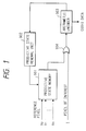
Fig. 1 shows an example of the encoding
circuit utilizing arithmetic codes.
The binary data I of an object pixel to be
encoded is supplied to an exclusive OR gate 904. Also
the binary data X of plural reference pixels in the
vicinity of the object pixel are supplied to a
predictive state memory 901, which supplies the
exclusive OR gate 904 with a predictive pixel data
"0" or "1" according to the state of the reference
pixel data. The exclusive OR gate 904 checks whether
the object pixel data I coincides with the predictive
pixel data from the predictive state memory 901, and
supplies an arithmetic encoder 903 with the result.
The arithmetic encoder 903 is provided with
an interval size register (A register) indicating
the current coding interval and a code register (C
register), and shifts the values of said A and C
registers according to the output of the exclusive
OR gate 904. Then values of consecutive 8 bits in a
specified position in said C register are outputted
as encoded data.
The content of the predictive state memory 901
is renewed according to an instruction of a prediction
renewal unit 902, receiving the result of encoding,
including the value of the A register of the arithmetic
encoder 903. Consequently, the predictive state memory
901 supplies the exclusive OR gate 904 with the
predictive pixel data adaptively to the current
encoding operation.
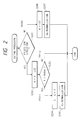
Fig. 2 is a flow chart of the encoding
operation of the encoder 903.
It is assumed that the A and C registers in
the encoder 903 have a capacity of 32 bits each, and a
section A is defined as 0 (0000H) - 0.5 (8000H) - 1.0
(10000H), wherein H stands for a hexadecimal number.
The exclusive OR gate 904 compares the object
pixel data with the predictive pixel data, and there
is discriminated whether both data mutually coincide
(S201). In case of coincidence, there is executed
re-normalization shown in Fig. 4, and, in case of non-coincidence,
there is executed re-normalization shown
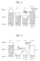
in Fig. 5. Fig. 3 shows the sequence of re-normalization.
The re-normalization shown in Fig. 3 is
executed in case the object pixel data and the
predictive pixel data do not mutually coincide, and
also in case both data mutually coincide and the value
A of the A register is less than 0.5 (8000H).
At first, in order to double the contents of
the A and C registers, the contents of said registers
are shifted by a bit in the direction of MSB, and the
count of a CT counter, counting the number of shifts,
is decreased by "1" (S301). In the present example, the
data in a specified position of the C register are taken
out as the encoded data at every eight shifts, in order
to handle the encoded data as 8-bit parallel data.
Thus a value "8" is initially set in the CT counter,
and said count is decreased stepwise at each 1-bit
shift of the A register. The 8-bit encoded data are
obtained when the count of the CT counter reaches "0".
Thus, there is discriminated whether the value
of the CT counter is "0" (S302), and, if "0", the 8-bit
encoded data are taken out from the C register and
released (S303), but, if not "0", the encoded data are
not outputted.
Then, it is discriminated whether the value A
of the A register, after 1-bit shift, is less than 0.5
(8000H) (S304), and, if not, the re-normalization is
terminated. On the other hand, if said value A of the
A register is less than 0.5 (8000H), the sequence returns
to the step S301 to effect again the 1-bit shifts of
the A and C registers and the stepwise subtraction of the
CT counter. These shifts are repeated until the value
A of the A register becomes no longer less than 0.5
(8000H).
In the following there will be explained the
transition of state of the A register in the re-normalization,
with reference to Figs. 4 and 5.
If the object pixel data coincides with the
predictive pixel data, a constant LSZ (least significant
coding interval) is subtracted from the value A of the
A register (S202). Then there is discriminated
whether the value A of the A register is smaller than
0.5 (8000H) (S203), and, if not, the encoding operation
is terminated through a path 2 ( phases 1, 2 in Fig. 4).
If the value A of the A register is smaller
than 0.5 (8000H), the sequence proceeds through a path
1 to add the value A of the A register to the value C
of the C register (S204). Then, the re-normalization
shown in Fig. 3 is executed in order to bring the value
A, which is less than 0.5 (8000H) to a value equal to
or larger than 0.5 (8000H), by shifting the A and C
registers (S205). In this manner the contents of the
A and C registers are renewed (phase 3 in Fig. 4).
In this state, the count of the CT counter, counting
the number of shifts of the A register, reaches "0",
whereupon the upper byte of the C register is outputted
as the encoded data.
On the other hand, if the object pixel data
does not coincide with the predictive pixel data, the
sequence proceeds through a path 3 to define the value
A of the A register as the constant LSZ (S206) and to
execute the re-normalization shown in Fig. 3 by
shifting the A register until the value A thereof
becomes equal to or larger than 0.5 (8000H) ( phases
1, 2, 3, 4 in Fig. 5). In the example shown in Fig.
5, the A register is shifted three times. In this
manner the content of the A register is renewed. The
C register is also likewise shifted. In the example
shown in Fig. 5, the count of the CT counter reaches
"0" at the first shift, whereupon the upper byte of
the C register is outputted as the encoded data, and
then the C register is set at "8".
In the above-explained encoding circuit
utilizing the arithmetic codes, the value C shifted in
the C register is outputted, in 8-bit unit, as the
encoded data. Said value C is added, as shown in the
step S204 in Fig. 2, to the value A. Consequently,
the addition of a certain value C and a certain value
A may result in a sum exceeding FFH. In such case,
the carry-over will influence at least the preceding
8-bit encoded data. Consequently the 8-bit data from
the C register cannot be directly supplied as the
encoded data to the transmission channel or the like,
and, if the addition of the values C and A may exceed
FFH and may result in a carry-over, such carry-over has
to be absorbed by a suitable method.
As a method for realizing this purpose, there
is known so-called carry-over waiting method in which
a code bit train outputted from the encoding register
is not transmitted but stored if it has the possibility
of carry-over.
This carry-over waiting method will be explained
in the following by an example.
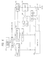
Fig. 6 shows a circuit for the carry-over
waiting method. In case of a re-normalization in an
arithmetic encoder 903, the output a thereof is
stored in a TEMP register 302. Said output a is a
9-bit data including carry-over. The output b of the
TEMP register 302 is the carry-over bit, and the
output c is an 8-bit data not including the carry-over
bit. The output b is supplied to carry-over
discrimination circuit 303, which releases an H (High)
level or an L (Low) level in the output j respectively
when the carry-over is present or absent. The output c
is supplied to an FF discrimination circuit 304 for
discriminating whether c is equal to FFH, and to a
buffer register 305 for storing the output c. The FF
discrimination circuit 304 releases a clock d for an
increment of an SC counter 306 in case c is equal to
FFH, and a clock e for storing c in the buffer register
305 in case c is not equal to FFH.
For the purpose of simplicity, the function
will be explained by an example.
It is assumed that the SC counter 306 has been
reset with an output k = 0, and that the buffer
register 305 stores C3H. At the next re-normalization,
the output of the arithmetic encoder 903 is stored in
a TEMP register 302, and said stored value is assumed
as BAH. In case of storage of BAH, since the carry-over
bit is not included, b is "0" and c is BAH.
Consequently the carry-over discrimination circuit
303 releases an output "L", and the FF discrimination
circuit 304 does not output the clock d for increment
of the SC counter 306 but releases the clock e for
storing the signal c in the buffer register 305.
An adder 307 executes a logic S = A + B.
Before the re-normalization, the buffer register 305
stores C3H, and, after the re-normalization, the
carry-over discrimination circuit 303 releases an
output j = L, so that a switch 308 is positioned at
the L-side while the adder 307 receives 00H at the
input B. Consequently the adder 307 releases an
output g = C3H.
A control circuit 309 outputs control signals
h, i determining the functions of switches 310, 311
according to the logic values of j, k. In case of j
= L, k = 00H, the signal i is L and the switch 311 is
positioned at the L side. Consequently there is
released a signal C3H is obtained at the output o.
In the following there will be explained
another case. In the above-explained sequence, let
us consider again the situation where the buffer
register stores C3H and the re-normalization has been
executed again. It is now assumed that the TEMP
register 302 stores FFH instead of BAH. Since there
is no carry-over, b = 0 and c = FFH. Since c = FFH,
the FF discrimination circuit 304 releases a clock d
for executing an increment of the SC counter 306.
However, there is not outputted the clock e for storing
the value of the TEMP register 302 into the buffer
register 305. Consequently the output f of the buffer
register 305 is still C3H. If the output of the
arithmetic encoder 903 at the next re-normalization
is still FFH, the SC counter 306 undergoes another
increment, while the buffer register 305 still stores
C3H. If said value FFH continues for n times of re-normalizations,
the output k of the SC counter 306
becomes n, while the output f of the buffer register
305 remains as C3H. It is now assumed that, at the
next re-normalization, 3EH is stored in the TEMP
register 302. Since there is no carry-over and no
coincidence with FFH, C3H is issued at the output o.
Thus the control circuit 309 outputs the signals h = L
and i = H. FFH is issued n times at the output o.
Then the SC counter 306 is reset, and 3EH is stored in
the buffer register 305. During said outputs of FFH
by n times, new encoded data cannot be fetched, so that
the preceding encoding process is temporarily suspended.
Let us consider still another case. Let us
consider again a situation where the buffer register
305 stores C3H and the SC counter 306 releases an
output n. It is now assumed that 13EH is stored in
the TEMP register 302 at the next re-normalization.
Said register 302 releases an output b = 1, so that
the carry-over discrimination circuit 303 identifies
the presence of carry-over to release an output j = H.
Thus, the switch 308 is shifted to the H side, and 01H
is supplied to the adder 307 which thus releases an
output g = C4H released from the output o. Subsequently,
the control circuit 309 shifts the signals h, i to H
level, and 00H is outputted n times according to the
count of the SC counter. The count of the buffer
register 302 becomes 3EH, and the SC counter 306 is
reset. Also during said output of 00H by n times,
the new encoded data cannot be fetched, so that the
preceding encoding process is temporarily suspended.
In the foregoing description, the count of the
SC counter 306 is assumed as n, but same explanation
can apply to any value of n equal to or larger than 0.
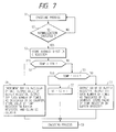
Fig. 7 is a flow chart showing the sequence of
the carry-over waiting method.
In synchronization with the re-normalization of
the A (Augent) register (S2), the data of the C (Code)
register are outputted in 8-bit (1 byte) unit or in
carry-over bit + 8-bit unit and are stored in the TEMP
register (S3). If the content of the TEMP register is
smaller than FFH (S4), said content is stored in the
buffer register. Since the next data to be outputted
from the C register may result in a carry-over, the
content of the buffer register is not outputted, but a
waiting state is entered (S6). If the next data
outputted from the C register and stored in the TEMP
register is smaller than FFH, there is no longer the
possibility of carry-over for the buffer register, so
that the content of the buffer register is outputted
as the encoded data, and the content of the TEMP
register is newly fetched in the buffer register.
Then, if the content of the TEMP register is
FFH (S5), the next data from the C register may
generate a carry-over, so that the content of the
buffer register cannot be outputted and the waiting
state is therefore continued (S7). In this state, the
count of the SC counter, indicating the number of
storages of FFH into the TEMP counter, is increased
by one. In case the data from the encoding register is
consecutively FFH, the output from the buffer register
is suspended, and the SC counter counts the number of
storages of FFH in the TEMP register. If the count of
the TEMP register in this state is smaller than FFH,
the carry-over is not generated, so that the content
of the buffer register is outputted. Thus FFH is
outputted by the number of times counted by the SC
counter, then the content of the TEMP register is
newly stored in the buffer register, and the SC
counter is cleared. If the content of the TEMP
register is larger than FFH, thus generating a carry-over
(S4), the carry-over propagates to the buffer
register. Thus there is outputted the content of
the buffer register + 1, and 00H is outputted by a
number of times counted by the SC counter. The buffer
register stores the content of the TEMP register,
excluding the carry-over bit, and the SC counter is
cleared (S8).
As will be apparent from the sequence shown in
Fig. 7, in the output of FFH by the number of times
counted by the SC counter in the step S6 or in the
output of 00H by the number of times counted by the SC
counter in the step S8, the next encoding process can
only be started after said output of FFH or 00H.
Consequently the encoding process is temporarily
suspended during such output of FFH or 00H by the number
of times counted by the SC counter.
In the above-explained encoding device of the
carry-over waiting method, if the carry-over propagates
to the released encoded data, the encoded data is
released by interrupting the encoding process. For
this reason such device has been associated with a
drawback of incapable of the real-time process
(for example in a facsimile apparatus, reading an
original document with a sensor and simultaneously
encoding the binarized data with an encoder), and it
has been necessary to interrupt the original reading
or to effect the encoding after the binarized data
are stored in a memory. For this reason there has
been required a long time for encoding, or a memory
for storing the binarized data.
In consideration of the foregoing, the present
invention is concerned with providing an image
encoding device enabling real-time process in
arithmetic encoding, and a method therefor.
Another concern of the present invention is to
provide an image encoding device capable of promptly
and efficiently executing the carry-over process in
the encoding utilizing arithmetic codes without
influencing the preceding encoding, and a method
therefor.
Still another concern of the present invention
is to provide an image encoding device capable of
executing the above-mentioned carry-over process,
without temporary interruption of the preceding encoding
process, and a method therefor.
Accordingly in one aspect of the present invention
provides an image encoding device as set out in claim 1.
According to a second aspect the present invention
comprises an image encoding method as set out in claim
7.
IBM Technical Disclosure Bulletin, Vol 23, No 1,
June 1980, New York US, pages 310-312 and US-A-4973961
both disclose data processing systems in which a count
is accumulated consisting of bytes of consecutive logical
1's and a carry-over process is carried out using the
accumulated count. Neither of these disclosures solve
the problem set out in the preamble of the present
specification, nor discloses the plurality of code latch
means and data latch means as set out in the independent
claim of the present case.
Still other concerns of the present invention, and
the features thereof, will become fully apparent from the
following description.
BRIEF DESCRIPTION OF THE DRAWINGS
Fig. 1 is a block diagram of an example of the
encoding circuit utilizing arithmetic codes;
Fig. 2 is a flow chart showing the encoding sequence
by arithmetic codes;
Fig. 3 is a flow chart showing the sequence of re-normalization
in arithmetic codes;
Figs. 4 and 5 are views showing re-normalizing
operations;
Fig. 6 is a block diagram of a circuit for
carry-over process in arithmetic codes;
Fig. 7 is a flow chart showing the sequence of
carry-over process;
Fig. 8 is a block diagram of an arithmetic
encoding circuit embodying the present invention;
Fig. 9 is a block diagram showing an example of
the priority encoder;
Fig. 10 is a chart showing the number of shifts
for re-normalization;
Fig. 11 is a block diagram showing the
configuration of a barrel shifter and an A register;
Fig. 12 is a chart showing values retained in a
CTV register;
Fig. 13 is a circuit diagram showing an example
of the carry-over control circuit of the present
invention; and
Fig. 14 is a circuit diagram showing another
example of the carry-over control circuit of the present
invention.
DESCRIPTION OF THE PREFERRED EMBODIMENTS
Now the present invention will be clarified in
detail by preferred embodiments thereof.
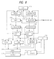
Fig. 8 shows the configuration of an encoder
embodying the present invention, and said encoder in
Fig. 8 is utilized as the encoder 903 in Fig. 1 to
constitute the image encoding device utilizing the
arithmetic codes.
There are provided a 16-bit C register 201;
a 16-bit A register 202 for storing data indicating the
current coding interval which is one of the parameters
employed for encoding of image data; barrel shifters
203, 204 respectively for bit shift of the C register
201 and the A register 202; and a CT register 205 for
retaining the CT value. In the configuration shown in
Fig. 8, there is employed a counter for subtraction,
but, the present embodiment utilizes a register for
retaining the entered CT value.
A priority encoder 206 receives the outputs
of the A register 202 and the CT register 205, controls
the shifts of the barrel shifters 203, 204 and also
controls a CT update logic 211 to renew the value of
the CT register 205. It also controls a high-byte
register 207 and a low-byte register 208 to control
the output of the upper and lower bytes stored in the
C register 201. There is also provided a carry-over
control circuit 209.
The content of the A register 202 is subjected,
in a subtractor 212, to the subtraction of LSZ from an
LSZ generator 213, and the result of said subtraction
is supplied to a selector 214. Said selector 214
also receives the LSZ from the LSZ generator 214.
The selector 214 selects either of the two inputs,
according to the output of an exclusive OR gate 904,
indicating coincidence or non-coincidence between
the object pixel and the predictive pixel. More
specifically, it selects the output (A - LSZ) from the
subtractor 214 in case of coincidence, or the LSZ
from the LSZ generator 213 in case of non-coincidence,
and the selected signal is supplied to the A register
202 to renew the content thereof.
Also the value of the C register 201 is added,
in an adder 215, to the output (A - LSZ) of the
subtractor 212 and is supplied to a gate 216, which
supplies the output of the adder 215 to the C register
201, in response to the output of the exclusive OR gate
904 indicating the non-coincidence between the object
pixel and the predictive pixel, whereby the content of
the C register is renewed.
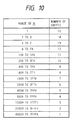
Since the value A of the A register at the execution
of re-normalization is with a range 1 ≦ A ≦ 7FFFH,
the number of bits of shift can be uniquely determined
according to the range of A, as shown in Fig. 10. This
can be represented as "finding '1' in a bit position
closest to the MSB side within the bits of A register".
Thus, the above-mentioned bit position can be detected
by a priority encoder 206 as shown in Fig. 9.
Referring to Fig. 9, the priority encoder 206
is composed of a logic circuit unit 509 and a 16 to 4
encoder 508. The bits stored in the A register 202
are taken out bit by bit in parallel manner, and supplied
to the logic circuit unit 509 composed of inverters 502,
504, 506,... and AND gates 503, 505, 507,... The
logic circuit unit 509 is so constructed that a high-level
output signal is obtained only from an AND gate,
among those 503, 505, 507,..., corresponding to '1' of
the bit position closest to the MSB, among those stored
in the A register 202. Thus, if the A register 202
stores data "0101...", the high-level output signal
is obtained only from the AND gate 503, corresponding
to the 2nd bit, or MSB - 1, of the A register 202.
The outputs of the AND gates 503, 505, 507,... are
supplied to the 16-to-4 encoder 508, which releases
4-bit data indicating the bit position.
Fig. 10 shows the correspondence between the
value of the A register 202 at the re-normalization
and the number of shifts of the A register 202.
The number of shifts from the priority encoder
206 is supplied to the barrel shifters 203, 204, which
accordingly shift the contents of the C register 201
and the A register 202 by 1 to 15 bits at a time.
Fig. 11 shows the structure of the barrel
shifter 204 and the A register 202. The barrel shifter
203 and the C register 201 are also constructed in the
same manner.
16-bit data stored in the A register 202 are
supplied in parallel manner to the barrel shifter 204.
The lower 15 bits of the barrel shifter 204 receive
"0".
The number of shifts from the priority encoder
206 is supplied to the barrel shifter 204, which
selects and outputs arbitrary data of consecutive 16
bits, among the 31-bit input, according to said number
of shifts. For example, if the priority encoder 26
enters a number of shifts of "3", the barrel shifter
204 selects N27, N26, N25,..., N12 from the input of
31 bits and releases said 16-bit data to the output
lines S15 to S0 in parallel manner.
The 16-bit data outputted in parallel manner
from the barrel shifter 204 are supplied in parallel
manner to the A register 202 and retained therein.
Consequently, a shift of the number of bits,
corresponding to the shift number instructed from the
priority encoder 206, can be executed at a time.
The update logic 211 receives the number of
shifts and the CT value before the re-normalization from
the priority encoder 206, and outputs the output byte
number and the CT value after the re-normalization.
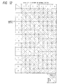
Fig. 12 shows a correspondence table provided
in the update logic 211. It will be understood that
an output byte number of 0 to 2 can be obtained,
depending on the number of shifts of 1 to 15 and the
CT value of 1 to 8. These values are used, in an
output control unit 210 shown in Fig. 8, for a control
of no output for a value "0", the output of the codes of
the high register 207 for a value "1", and the output of
two bytes of the high-byte register 207 and the low-byte
register 208 for a value "2".
Also the update logic 211 supplies the CT
register 205 with a new CT value, which is retained
therein.
As explained in the foregoing, the plural bit
values in the A register 202 are monitored in parallel
manner, and, at the re-normalization, the shifts of
plural bits in the A register 202 and the C register
201 are executed at a time. In this manner the time
required for the re-normalization can be made constant
regardless whether the object pixel data to be encoded
coincides with the predictive pixel data and regardless
of the content of the A register, so that the real-time
synchronous encoding of the object pixel data to be
encoded can be realized.
Fig. 13 shows the structure of the carry-over
control circuit 209 in Fig. 8, where in provided are
flip-flops (F/F) 100 to 104, 110 to 114, 120 to 124
and 129; multiplexers or switches 105 to 109, 115 to
118 and 125 to 128; AND gates 131, 133, 134, 136, 137,
139, 140, 142 and 143; inverters 132, 135, 138, 141
and 144; a register 130 corresponding to the high-byte
register 207 and the low-byte register 208 in
Fig. 8; an adder 150; and an FF discrimination circuit
160. The broken-lined portion indicates repetition
of similar circuits, consisting of serial connection
of a required number of the circuit 170 framed in in a
chain-lined frame.
The functions of the above-explained circuitry
will be explained in the following. The register 130
releases a code train according to the above-explained
encoding sequence and in synchronization with the
re-normalization, wherein a is the carry-over data and
b is data of at least a bit, excluding the carry-over.
In the following description, the data b is assumed
to be of 8 bits, as in the foregoing description.
The flip-flops (F/F) 100 to 104, 110 to 114,
120 to 124 and 129 latch the input data in
synchronization with the re-normalization. Consequently
the data are shifted from left to right, at each re-normalization.
For the purpose of simplicity, the
circuit 170 is assumed to be repeated 5 times so that
the total number of shifts is five.
Also the code trains released from the
register 130 at the re-normalizations are assumed to
be C3H, BAH, FFH, FFH, 1AEH,...
Prior to the encoding, the flip-flops (F/F)
100 to 104 are reset.
At the first re-normalization, the register
130 releases an output C3H without carry-over, so
that the output a is "0" and the output b is C3H.
The output b is latched in the F/F 120. The FF
discrimination circuit 160, for discriminating whether
the output b is equal to FFH, upon receiving C3H,
releases an output "0", which is latched in the F/F
100. Also since the output a is "0", the AND gate
131 releases an output "0" whereby the switch 109 is
shifted to the L-side and the value "0" is latched
in the F/F 110.
At the second re-normalization, the register
130 releases an output BAH, so that the output a is
"0" and the output b is BAH. Through operations
similar to those in the first re-normalization, the
F/F 100 releases an output "0", the F/F 110 releases an
output "0" and the F/F 120 releases an output BAH.
Also by shift operations, the F/F 101 releases an
output "0", the F/F 111 releases an output "0" and the
F/F 121 releases an output C3H.
At the third re-normalization, the register
130 releases an output FFH, so that the output a is
"0" and the output b is FFH. The output b, being
FFH, is discriminated as equal to FFH in the FF
discrimination circuit 160, which therefore releases
an output "1", which is latched in the F/F 100. Thus
there are obtained outputs "1" from F/F 100, "0" from
F/F 110, FFH from F/F 120, "0" from F/F 101, "0" from
F/F 111, BAH from F/F 121, "0" from F/F 102, "0" from
F/F 112, and C3H from F/F 122.
At the fourth re-normalization, the register
130 releases an output FFH, so that the output a is
"0" and the output b is FFH. In a similar manner
there are obtained outputs "1" from F/F 100, "0" from
F/F 110, FFH from F/F 120, "1" from F/F 101, "0" from
F/F 111, FFH from F/F 121, "0" from F/F 102, "0"
from F/F 112, BAH from F/F 122, "0" from F/F 103, "0"
from F/F 113 and C3H from F/F 123.
At the fifth re-normalization, the register
130 releases lAEH including a carry-over, so that the
output a of the register 130 is "1" and the output b
is AEH. Since the F/ F 100, 101 release "1" in this
state, the AND gates 131, 134 release outputs "0"
which are latched in the F/ F 110, 111. Also since
the F/ F 100, 101 release outputs "1" while the F/F
102 releases an output "0", the carry-over signal from
the register 130 is transmitted through the AND gates
133, 136 and 137, whereby the switch 116 is shifted to
the H-side and the signal "1" is latched in the F/F 112.
Also since the AND gates 133, 136 release outputs "1",
the switches 105, 106 are shifted to the H-side whereby
the F/ F 101, 102 latch "0". Similarly the switches 125,
126 are shifted to the H-side, whereby the F/ F 121, 122
latch 00H. Consequently, there are obtained the
following outputs "0" from F/F 100, "0" from F/F 110,
AEH from F/F 120, "0" from F/F 101, "0" from F/F 111,
00H from F/F 121, "0" from F/F 102, "1" from F/F 112,
00H from F/F 122, "0" from F/F 103, "0" from F/F 113,
BAH from F/F 123, "0" from F/F 104, "0" from F/F 114,
and C3H from F/F 124.
At the next re-normalization, the F/F 129
releases an output C3H while the F/F 114 releases an
output "0". Because there is no carry-over, the adder
150 releases an output C3H, which is outputted as
established code output. At the next re-normalization,
the F/F 129 releases an output BAH while the F/F 114
releases an output "1". Because there is a carry-over,
the adder 150 releases an output BBH, which is outputted
as an established code output. At the next re-normalization,
the F/F 129 outputs 00H while the F/F
114 releases an output "0". Because there is no
carry-over, the adder 150 releases an output 00H, which
is outputted as the established code output. At the
next re-normalization, the F/F 129 releases an output
00H, while the F/F 114 releases an output "0". Since
there is no carry-over, the adder 150 releases an
output 00H, which is outputted as the established code
output.
Thereafter, the operations are conducted in
similar manner to obtain established code outputs.
In the embodiment shown in Fig. 13, the
output of the arithmetic encoder is assumed to be based
on positive logic, but a similar object can be
attained naturally through negative logic. Also the
logic circuit composed of the multiplexers (switches),
AND gates and inverters is not limited to that shown
in Fig. 13, but an equivalent function can be attained
by other logic circuits.
As explained in the foregoing, there are
retained plural sets of code data, generated in
succession in the unit of a predetermined number of
bits (8 bits in this embodiment), and, in case a carry-over
is generated, such carry-over is immediately
absorbed by thus retained plural sets of code data.
Consequently, the carry-over processing can be promptly
executed without a particular interruption. Thus,
such carry-over process avoids the influence on the
preceding encoding process and enables efficient
execution of such encoding process.
Also the foregoing embodiment enables, in the
waiting method for the output of the arithmetic
encoder, to dispense with the SC counter for counting
the number of generation of the encoded data FFH.
Fig. 14 shows another embodiment of the carry-over
process circuit 209, wherein provided are flip-flops
410 to 414, 420 to 424 and 429; multiplexers or
switches 409, 415 to 418, 425 to 428; AND gates 431,
433, 434, 436, 437, 439, 440, 441, 443 and 444;
inverters 432, 435, 438, 442 and 445; a register 430
corresponding to the high-byte register 207 and the
low-byte register 208 in Fig. 8; an adder 450; and
FF discrimination circuits 460 to 464. The broken-lined
portion indicates repetition of similar
circuits, consisting of serial connection of a
required number of the circuit 470 surrounded in a
chain-lined frame.
It is different from the embodiment shown in
Fig. 13, in that the FF discrimination circuit, for
discriminating whether the output data of the
register 430 is FFH, is provided at each output of
the flip-flops 421 to 424, and this difference will
be clarified further in the following description
based on the same assumptions and conditions as in
the foregoing description.
At the first re-normalization, the register
430 releases an output C3H without the carry-over,
so that the output a is "0" and the output b is C3H.
The output b is latched in the F/F 420. Since the AND
gate 431 releases an output "0", the switch 409 is
shifted to the L-side, and the F/F 410 latches "0".
At the second re-normalization, the register
430 releases an output BAH, so that the output a is
"0" and the output b is BAH. Through operations
similar to those in the first re-normalization, the
F/F 410 releases an output "0", while the F/F 420
releases an output BAH. Also through shift operations,
the F/F 411 releases an output "0", and the F/F 421
releases an output C3H.
At the third re-normalization, the register
430 releases an output FFH, so that the output a is
"0" and. the output b is FFH. There are consequently
obtained the following outputs: "0" from F/F 410,
FFH from F/F 120, "0" from F/F 411, BAH from F/F 421,
"0" from F/F 412, and C3H from F/F 422.
At the fourth re-normalization, the register
430 releases an output FFH, so that the output a is
"0" and the output b is FFH. There are obtained the
following outputs: "0" from F/F 410, FFH from F/F 420,
"0" from F/F 411, FFH from F/F 421, "0" from F/F 412,
BAH from F/F 422, "0" from F/F 413, and C3H from F/F
423.
At the fifth re-normalization, the register
430 releases an output lAEH including a carry-over,
so that the output a is "1" and the output b is AEH.
The FF discrimination circuits 460, 461, for respectively
discriminating whether the outputs of the F/ F 420, 421
are equal to FFH, upon receiving the outputs FFH from
said F/ F 420, 421, release outputs "1". Also since
the output a is "1", the AND gates 433, 436 release
outputs "1", whereby the switches 425, 426 are shifted
to the H-side and the F/ F 421, 422 latch "0". Also
since the F/F 422 latches BAH, the FF discrimination
circuit 462 releases an output "0", whereby the AND
gate 437 releases an output "1" and the F/F 412 latches
"1". Consequently, there are obtained the following
outputs: "0" from F/F 410, AEH from F/F 420, "0"
from F/F 411, 00H from F/F 421, "1" from F/F 412,
00H from F/F 422, "0" from F/F 413, BAH from F/F 423,
"0" from F/F 414, and C3H from F/F 424.
At the next re-normalization, the F/F 429
releases an output C3H, while the F/F 414 releases
an output "0". Since there is no carry-over, the
adder 450 releases an output C3H, which is outputted
as an established code output. Then, at the next
re-normalization, the F/F 429 releases an output BAH
while the F/F 414 releases an output "1". Since there
is a carry-over, the adder 450 releases an output BBH,
which is outputted as an established code output.
At the next re-normalization, the F/F 429
releases an output 00H while the F/F 414 releases an
output "0". Since there is no carry-over, the adder
450 releases an output 00H, which is released as an
established code output. At the next re-normalization,
the F/F 420 releases an output 00H, while the F/F 414
releases an output "0". Since there is no carry-over,
the adder 450 provides an output 00H, which is
outputted as the established code output.
Thereafter, similar operations are executed
to provide established code outputs.
As explained in the foregoing, there is
provided means for delaying the code data trains,
obtained by arithmetic codes, by plural steps by means
of shift registers, and generating carry-over
information and renewal code data by means of thus
delayed code data trains. Thus, the carry-over can
be absorbed by thus delayed code data trains, so that
the carry-over process can be executed without the
waiting time, and the arithmetic encodint can be
realized on real-time basis.
Also since the SC counter, for counting the
number of FFH in the code data train, can be dispensed
with, there can be obtained a code train including the
carry-over process, without interruption in the function
of the arithmetic encoder. Because of absence of
interruption in the function of the arithmetic encoder,
the data (for example binary image data) supplied to
the arithmetic encoder can be encoded on real-time
basis.
Also since the arithmetic encoder can be
realized with a circuit configuration synchronized
with the input data, the arithmetic encoder can be
designed more easily and in a more simplified manner.
The present invention has been explained by
preferred embodiments thereof, but it is naturally
not limited to such embodiments and is subject to
various modifications within the scope of
the appended claims.