EP0595251B1 - A serial access memory - Google Patents
A serial access memory Download PDFInfo
- Publication number
- EP0595251B1 EP0595251B1 EP93117304A EP93117304A EP0595251B1 EP 0595251 B1 EP0595251 B1 EP 0595251B1 EP 93117304 A EP93117304 A EP 93117304A EP 93117304 A EP93117304 A EP 93117304A EP 0595251 B1 EP0595251 B1 EP 0595251B1
- Authority
- EP
- European Patent Office
- Prior art keywords
- address
- output
- serial
- access memory
- circuit
- Prior art date
- Legal status (The legal status is an assumption and is not a legal conclusion. Google has not performed a legal analysis and makes no representation as to the accuracy of the status listed.)
- Expired - Lifetime
Links
Images


Classifications
-
- G—PHYSICS
- G09—EDUCATION; CRYPTOGRAPHY; DISPLAY; ADVERTISING; SEALS
- G09G—ARRANGEMENTS OR CIRCUITS FOR CONTROL OF INDICATING DEVICES USING STATIC MEANS TO PRESENT VARIABLE INFORMATION
- G09G3/00—Control arrangements or circuits, of interest only in connection with visual indicators other than cathode-ray tubes
- G09G3/20—Control arrangements or circuits, of interest only in connection with visual indicators other than cathode-ray tubes for presentation of an assembly of a number of characters, e.g. a page, by composing the assembly by combination of individual elements arranged in a matrix no fixed position being assigned to or needed to be assigned to the individual characters or partial characters
- G09G3/34—Control arrangements or circuits, of interest only in connection with visual indicators other than cathode-ray tubes for presentation of an assembly of a number of characters, e.g. a page, by composing the assembly by combination of individual elements arranged in a matrix no fixed position being assigned to or needed to be assigned to the individual characters or partial characters by control of light from an independent source
- G09G3/36—Control arrangements or circuits, of interest only in connection with visual indicators other than cathode-ray tubes for presentation of an assembly of a number of characters, e.g. a page, by composing the assembly by combination of individual elements arranged in a matrix no fixed position being assigned to or needed to be assigned to the individual characters or partial characters by control of light from an independent source using liquid crystals
- G09G3/3611—Control of matrices with row and column drivers
- G09G3/3622—Control of matrices with row and column drivers using a passive matrix
- G09G3/3644—Control of matrices with row and column drivers using a passive matrix with the matrix divided into sections
-
- G—PHYSICS
- G09—EDUCATION; CRYPTOGRAPHY; DISPLAY; ADVERTISING; SEALS
- G09G—ARRANGEMENTS OR CIRCUITS FOR CONTROL OF INDICATING DEVICES USING STATIC MEANS TO PRESENT VARIABLE INFORMATION
- G09G5/00—Control arrangements or circuits for visual indicators common to cathode-ray tube indicators and other visual indicators
- G09G5/36—Control arrangements or circuits for visual indicators common to cathode-ray tube indicators and other visual indicators characterised by the display of a graphic pattern, e.g. using an all-points-addressable [APA] memory
- G09G5/39—Control of the bit-mapped memory
-
- G—PHYSICS
- G11—INFORMATION STORAGE
- G11C—STATIC STORES
- G11C7/00—Arrangements for writing information into, or reading information out from, a digital store
- G11C7/10—Input/output [I/O] data interface arrangements, e.g. I/O data control circuits, I/O data buffers
- G11C7/1015—Read-write modes for single port memories, i.e. having either a random port or a serial port
- G11C7/103—Read-write modes for single port memories, i.e. having either a random port or a serial port using serially addressed read-write data registers
-
- G—PHYSICS
- G11—INFORMATION STORAGE
- G11C—STATIC STORES
- G11C7/00—Arrangements for writing information into, or reading information out from, a digital store
- G11C7/10—Input/output [I/O] data interface arrangements, e.g. I/O data control circuits, I/O data buffers
- G11C7/1051—Data output circuits, e.g. read-out amplifiers, data output buffers, data output registers, data output level conversion circuits
- G11C7/1069—I/O lines read out arrangements
-
- G—PHYSICS
- G11—INFORMATION STORAGE
- G11C—STATIC STORES
- G11C8/00—Arrangements for selecting an address in a digital store
- G11C8/10—Decoders
-
- G—PHYSICS
- G11—INFORMATION STORAGE
- G11C—STATIC STORES
- G11C8/00—Arrangements for selecting an address in a digital store
- G11C8/18—Address timing or clocking circuits; Address control signal generation or management, e.g. for row address strobe [RAS] or column address strobe [CAS] signals
-
- G—PHYSICS
- G09—EDUCATION; CRYPTOGRAPHY; DISPLAY; ADVERTISING; SEALS
- G09G—ARRANGEMENTS OR CIRCUITS FOR CONTROL OF INDICATING DEVICES USING STATIC MEANS TO PRESENT VARIABLE INFORMATION
- G09G2360/00—Aspects of the architecture of display systems
- G09G2360/12—Frame memory handling
- G09G2360/126—The frame memory having additional data ports, not inclusive of standard details of the output serial port of a VRAM
-
- G—PHYSICS
- G09—EDUCATION; CRYPTOGRAPHY; DISPLAY; ADVERTISING; SEALS
- G09G—ARRANGEMENTS OR CIRCUITS FOR CONTROL OF INDICATING DEVICES USING STATIC MEANS TO PRESENT VARIABLE INFORMATION
- G09G3/00—Control arrangements or circuits, of interest only in connection with visual indicators other than cathode-ray tubes
- G09G3/20—Control arrangements or circuits, of interest only in connection with visual indicators other than cathode-ray tubes for presentation of an assembly of a number of characters, e.g. a page, by composing the assembly by combination of individual elements arranged in a matrix no fixed position being assigned to or needed to be assigned to the individual characters or partial characters
- G09G3/34—Control arrangements or circuits, of interest only in connection with visual indicators other than cathode-ray tubes for presentation of an assembly of a number of characters, e.g. a page, by composing the assembly by combination of individual elements arranged in a matrix no fixed position being assigned to or needed to be assigned to the individual characters or partial characters by control of light from an independent source
- G09G3/36—Control arrangements or circuits, of interest only in connection with visual indicators other than cathode-ray tubes for presentation of an assembly of a number of characters, e.g. a page, by composing the assembly by combination of individual elements arranged in a matrix no fixed position being assigned to or needed to be assigned to the individual characters or partial characters by control of light from an independent source using liquid crystals
- G09G3/3611—Control of matrices with row and column drivers
Definitions
- This invention relates to a semiconductor memory, and particularly to a serial access memory that can be used in image processing and operated at a high speed.
- a serial access memory has been widely used for image processing in personal computers, word processors and the like.
- the serial access memory employed in image processing needs a high image-drawing speed.
- a device is normally used wherein a serial access memory is electrically connected to a general-purpose dynamic random access memory (hereinafter called a "DRAM").
- DRAM general-purpose dynamic random access memory
- This type of device writes data into the DRAM and thereafter reads data corresponding to a desired row, one row at a time. Then, the read data are transferred to the serial access memory, from which the data are serially read.
- US-A-4,450,538 discloses an address accessed memory device having parallel to serial conversion.
- a memory device is provided with first and second memories.
- Two groups of data are loaded into the first and second memories, through a data buffer register.
- the same address information is applied to the first and second memories and the information is read out from the first and second memories.
- the two groups of the data read out in parallel are applied to a data multiplexer which in turn converts the parallel information into the serial one.
- EP-A-0 174 845 discloses a semiconductor memory device.
- the semiconductor memory device can continuously read or store a plurality of data therefrom or therein.
- the semiconductor memory device includes a memory unit having a plurality of memory cells, the memory cells being arranged in a matrix having rows and columns, and a reading storing circuit.
- the reading storing circuit can read or store data from or into the memory cell at an address corresponding to an address signal received therein in response to the reception of first and second control signals, respectively.
- the reading storing circuit also can consecutively read or store data from or into the memory cell at another address subsequent to the address read or stored at the last time in response to the reception of the second control signal.
- Such a device can therefore have improved access time for continuous accessing of a plurality of data.
- STN Super Twined Nematic
- LCD liquid crystal display
- OA office automation
- the present invention provides a serial access memory comprising first and second memory cell arrays, which memory is provided with a control circuit for controlling the Most Significant Bit (MSB) of an addess supplied to each of the first and second memory cell arrays. That is, a MSB control circuit is provided which is capable of making the MSB of each address appear invalid when data is transferred from each memory cell array. Owing to the provision of the MSB control circuit, the operations of circuits in the first memory cell array become identical to those of circuits in the second memory cell array.
- MSB Most Significant Bit
- serial access memory of the present invention when applied to the STN type LCD, a display device can be materialized which is capable of easily producing memory maps in memory cells and making it unnecessary to provide externally-mounted elements such as a multiplexer, etc.
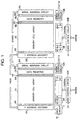
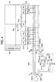
- FIG. 1 is a block diagram showing the structure of the serial access memory of the present invention.
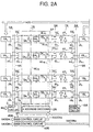
- FIG. 2 is a block diagram illustrating, in detail, the structure of a principal part of the serial access memory shown in FIG. 1. Elements shown in FIG. 2, which are common to those shown in FIG. 1 are identified by the same reference numerals as those employed in FIG. 1.
- the serial access memory has a first memory cell array 1A and a second memory cell array 1B.
- X address decoders 2A and 2B are respectively electrically connected to the memory cell arrays 1A and 1B.
- the X address decoder 2A is electrically connected to the word lines WLai and WLaj of the array 1A.
- the X address decoder 2A has a function to decode 0th to N-1th X addresses XADDAa (binary values 0 to N-1) of an ordered X address group XADD and selecting a desired column from the memory cell array 1A.
- the X address decoder 2B is electrically connected to the word lines WLai and WLaj of the array 1B.
- the X address decoder 2B has a function to decode Nth to 2N-1th X addresses XADDBa (binary values N to 2N-1) of the X address group XADD and selecting a desired column from the memory cell array 1B.
- An input circuit 3 is of a circuit for inputting write data inputted from an input terminal IN to the memory arrays 1A and 1B via respective write data buses 4A and 4B.
- the Y address decoders 5A and 5B respectively have functions to decode the common Y address group YADD and select desired rows from the respective memory cell arrays 1A and 1B. Data on the write data buses are input to the selected rows.
- the transistor pairs trc i and trc i are controlled in accordance with a data transfer signal DT.
- Each of the read transfer circuits 6A and 6B has a function to transfer data corresponding to one column selected from each of the memory cell arrays 1A and 1B, to the respective data registers 7A and 7B, in response to the data transfer signal DT.
- Each of the flip-flops FF i is made up of two inverters inversely parallel-connected to each other.
- Each of the data registers 7A and 7B has a function for storing therein read data corresponding to one column, which is transferred from each of the read transfer circuits 6A and 6B.
- the data registers 7A and 7B are respectively electrically connected to serial address circuits 8A and 8B. Further, the data registers 7A and 7B are also electrically connected to their corresponding serial output circuits 10A and 10B via read data buses 9A and 9B respectively.
- the transistor pairs trd i and trd i of the respective circuits 8A and 8B are respectively electrically connected between the flip-flops FF i of the respective data registers 7A and 7B and the respective read data buses 9A and 9B. Desired transistor pairs are respectively selected based on outputs yb i produced from the unit serial address decoders YB i .
- Each of the serial address circuits 8A and 8B has a function to serially output read data corresponding to one column, which has been stored in each of the data registers 7A and 7B, to each of the read data buses 9A and 9B.
- Each of the serial address circuits 8A and 8B may be constructed of a shift register that is shift-activated in response to a synchronizing clock signal or a serial address pointer.
- serial output circuits 10A and 10B serially output read data that has been respectively transmitted over the respective read data buses 9A and 9B, from the respective output terminals OUTA and OUTB, in response to a synchronizing control clock signal (the outputs from the serial output circuits 10A and 10B correspond to serial data).
- a first most significant bit (hereinafter abbreviated as "MSB") control circuit 40A and a second MSB control circuit 40B are respectively electrically connected to the X address decoders 2A and 2B.
- the first MSB control circuit 40A is supplied with an X address group XADDA.
- the first MSB control circuit 40A has a function to supply an X address group XADDAa which makes the MSB of the X address group XADDA appear invalid to the X address decoder 2A, in response to the data transfer signal DT supplied when the transfer of data from the memory cell arrays 1A and 1B to the corresponding data registers 7A and 7B is performed.
- the second MSB control circuit 40B is supplied with an X address group XADDB.
- the second MSB control circuit 40B has a function to supply an X address group XADDBa which makes the MSB of the X address group XADDB appear invalid to the X address decoder 2B, in response to the data transfer signal DT.
- first and second MSB control circuits 40A and 40B Configurations of the first and second MSB control circuits 40A and 40B will hereinafter be described in detail. Since the first MSB control circuit 40A is identical in circuit configuration to the second MSB control circuit 40B, a description will hereinafter be made of the first MSB control circuit 40A alone. It is apparent that the second MSB control circuit 40B also can be easily understood from the following description.
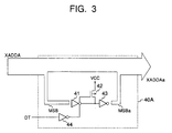
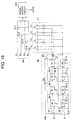
- FIG. 3 is a circuit diagram schematically showing the first MSB control circuit 40A.
- the first MSB control circuit 40A comprises a tristate inverter 41 supplied with the MSB of the X address group XADDA input from an external source, a P channel MOS transistor (hereinafter abbreviated as "PMOS") 42 electrically connected to the output of the tristate inverter 41, for preventing the occurrence of a floating state, an inverter 43 electrically connected to the output of the tristate inverter 41 and the drain electrode of the PMOS 42, and an inverter 44 for controlling the tristate inverter 41 in response to the data transfer signal DT.
- PMOS P channel MOS transistor
- the MSB of the X address group XADDA is input to the tristate inverter 41.
- a logical level of the data transfer signal DT is brought to a high (hereinafter abbreviated as "H") level
- the output of the inverter 44 is brought to a low (hereinafter abbreviated as "L") level.
- the output of the tristate inverter 41 is brought into a high-impedance state. Since, at this time, the PMOS 42 is turned ON in response to the output (“L") of the inverter 44, the input of the inverter 43 is brought to a power source potential VCC.
- the output MSBa of the inverter 43 is forcibly brought to the "H" level.
- the first MSB control circuit 40A outputs internal addresses, i.e., the X address group XADDAa.
- the tristate inverter 41 serves as an inverter which simply performs an inversion operation. Accordingly, the MSB of the X address group XADDA is inverted by the tristate inverter 41 and the output of the tristate inverter 41 is inverted by the inverter 43.
- the output MSBa of the inverter 43 is a signal having the same phase as that of the MSB.
- the MSB of the X address group XADDB is input to the tristate inverter 41.
- the output of the inverter 44 is brought to a low (hereinafter abbreviated as "L") level when the logical level of the data transfer signal DT is high (hereinafter abbreviated as "H") .
- L low
- H logical level of the data transfer signal DT
- the output of the tristate inverter 41 is brought to a high-impedance state. Since, at this time, the PMOS 42 is turned ON in response to the low (“L") output of the inverter 44, the input of the inverter 43 is brought to the power source potential VCC.
- the output MSBb of the inverter 43 is forcibly brought to the "H" level.
- the second MSB control circuit 40B outputs internal addresses, i.e., the X address group XADDBa.
- the tristate inverter 41 serves as an inverter which simply performs an inversion operation. Accordingly, the MSB of the X address group XADDB is inverted by the tristate inverter 41 and the output of the tristate inverter 41 is inverted by the inverter 43.
- the output MSBb of the inverter 43 is a signal whose phase is identical to that of the MSB.
- first and second MSB control circuits 40A and 40B and their peripheral circuits will hereinafter be described in detail with reference to FIG. 4.
- first MSB control circuit 40A is identical in structure to the second MSB control circuit 40B. Therefore, only the first MSB control circuit 40A will be described below.
- the second MSB control circuit 40B will be easily understood from the following description.
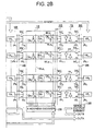
- An X address circuit 2A comprises a gate circuit 2-1 made up of n AND gates (AND 1 to AND n ) and an X decoder 2-2 made up of n unit X decoders XD 1 to XD n which are composed principally of NAND gates. Each unit decoder XD i is electrically connected to its corresponding word line WLa i . Thus, a desired address is selected from complementary addresses B 0 , B 0 to B n-1 , B n-1 forming the X address group XADDAa by the gate circuit 2-1 so as to be input to the X decoder 2-2.
- the complementary addresses B n-1 and B n-1 of the X address group XADDAa correspond to the MSBa.
- the first MSB control circuit 40A outputs complementary addresses A 0 , A 0 to A n-2 , A n-2 as the addresses B 0 , B 0 to B n-2 , B n-2 as they are, exclusive of the A n-1 , A n-1 corresponding to the MSB.
- the complementary addresses A n-1 , A n-1 of the X address group XADDA, which correspond to the MSB, are input to tristate inverters 41-1 and 41-2 respectively. Then, the first MSB control circuit 40A outputs the complementary addresses B n-1 , B n-1 therefrom in response to the data transfer signal DT.
- the first MSB control circuit 40A converts the complementary addresses A n-1 , A n-1 into the complementary addresses B n-1 , B n-1 and outputs the latter therefrom.
- the data transfer signal DT is of the "L" state
- the logical level of the data transfer signal DT is inverted by the inverter 44.
- the tristate inverters 41-1 and 41-2 performs normal inversion operations. Therefore, the MSB or addresses A n-1 , A n-1 are inverted by the tristate inverters 41-1 and 41-2 and thereafter inverted by inverters 43-1 and 43-2.
- the first MSB control circuit 40A outputs the complementary addresses B n-1 , B n-1 (MSBa), which are respectively in phase with the complementary addresses A n-1 , A n-1 corresponding to the MSB.
- MSBa complementary addresses
- the data transfer signal DT is of the "H" state
- the logical level of the data transfer signal DT is inverted by the inverter 44.
- each of the outputs of the tristate inverters 41-1 and 41-2 is brought into a high-impedance state. Since PMOSs 42-1 and 42-2 are turned ON in response to the low ("L") output of the inverter 44, the complementary addresses B n-1 , B n-1 are both brought to the "H" level.
- an input terminal of the gate circuit 2-1 supplied with the addresses MSBa (B n-1 , B n-1 ), is brought to the "H” level. That is, one of the inputs of one of the AND gates in the gate circuit 2-1 is brought to the "H” level.
- the second MSB control circuit 40B is supplied with the X address group XADDB.
- the first MSB control circuit 40B has a function to supply an X address group XADDBa which makes the MSB of the X address group XADDB appear invalid to the X address decoder 2B, in response to the data transfer signal DT.
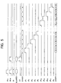
- the operation of the above-described serial access memory will be described below with reference to a timing chart shown in FIG. 5.
- the operation of the first memory cell array 1A is basically identical to that of the second memory cell array 1B. Therefore, a typical operation of the first memory cell array 1A will be described below.
- the operation of the second memory cell array 2B also will be easily understood from the following description.
- the first MSB control circuit 40A in the serial access memory of the present invention is supplied with 0th to N-1th X addresses XADDA of the X address group XADD, whereas the second MSB control circuit 40B is supplied with Nth to 2N-1th X addresses XADDB of the X address group XADD.
- the first and second MSB control circuits 40A and 40B convert the respective X address groups XADDA and XADDB into respective internal X address groups XADDAa and XADDBa and output them to the respective X address decoders 2A and 2B.
- the X address group XADDA is supplied to the first MSB control circuit 40A and the Y address group YADD is supplied to the Y address decoder 5A.
- the write data is input from the input terminal IN. Since the data transfer signal DT is in the "L" state, the input X address group XADDA is sent to the X address decoder 2A via the first MSB control circuit 40A as the X address group XADDAa having the same addresses as those in the X address group XADDA.
- the X address decoder 2A decodes the X address group XADDAa and sets a desired word line WLa i at the "H" level, so as to select a desired column. Thus, transistors in each of the memory cell Qk i electrically connected to the word line WLa i are turned ON. Further, the unit Y decoder YA i in the Y address decoder 5A decodes the Y address group YADD so as to bring an output ya n-1 of a desired unit Y decoder YA n-1 to the "H" level. Therefore, a pair of transistors tra n-1 and tra n-1 is turned ON.
- the write data bus 4A and the paired bit lines BLa n-1 , BLa n-1 are electrically connected to each other, the write data input from the input terminal IN is sent to the paired bit lines BLa n-1 , BLa n-1 via the input circuit 3 and the write data bus 4A. As a result, the write data is written into the memory cell Qk n-1 .
- the MSB control circuits 40A and 40B are activated in response to the data transfer signal DT so as to output the X address groups XADDAa and XADDBa, which make the MSB's of the X address groups XADDA and XADDB invalid, to the respective X address decoders 2A and 2B. Therefore, the X address decoders 2A and 2B become identical to each other in their circuit operation.
- the X address group XADDAa input to the X address decoder 2A and the X address group XADDBa input to the X address decoder 2B become equal to each other by the first and second MSB control circuits 40A and 40B.
- the identical columns are respectively selected from the memory cell arrays 1A and 1B as shown in FIG. 6A. This will be described specifically by the following simple example.
- the X address groups XADDAa and XADDBa which have made the MSBs of the respective address groups invalid, are both brought to the same values, i.e., "x0001, x00010, x00011 to x1111".
- the term "x” means that the MSB's have been made invalid. That is , the MSB's can be made invalid by bringing one of the inputs of the gate circuit 2-1 into the "H" state.
- the first MSB control circuit 40A When the 0th to N-1th X addresses XADDA of the X address group XADD are supplied to the first MSB control circuit 40A during a transfer cycle, the first MSB control circuit 40A outputs the X address group XADDAa, which makes the MSB of the X address group XADDA invalid, to the X address decoder 2A.
- the X address decoder 2A selects a desired word line WLa i based on the X address group XADDAa.
- the data stored in the memory cell QK i which is electrically connected to the selected word line WLa i is output to the bit line BLa i . Thereafter the output data is amplified by the corresponding sense amplifier SA i .
- the second MSB control circuit 40B invalidates its MSB to form the X address group XADDBa is identical to the X address group XADDAa, and outputs the same to the X address decoder 2B.
- the X address decoder 2B selects a desired word line WLa i from the memory cell array 1B, corresponding to the selected line of memory cell array 1A, based on the X address group XADDBa.
- the data stored in the memory cell Qk i electrically connected to the selected word line WLa i is output to the paired bit lines BLa i , BLa i , and is thereafter amplified by the corresponding sense amplifier SA i , similarly to the outputting and amplification of data in memory cell array 1A. Since, at this time, the data transfer signal DT is in the "H" state, the read transfer circuits 6A and 6B are both brought into an ON state.
- the amplified data on the bit line pairs BLa i , BLa i in the respective memory cell arrays 1A and 1B are respectively transferred to the data registers 7A and 7B at the same time, and stored in the corresponding flip-flops FF i of the data registers 7A and 7B as shown in FIG. 6B.
- serial address group SYADD When the serial address group SYADD is then supplied to the serial address circuits 8A and 8B, it is decoded by the serial address circuits 8A and 8B. Further, the outputs yb i of the unit serial address decoders YB i are successively brought to the "H" level. As a result, the transistor pairs trd i and trd i are successively turned ON. Thus, the read data stored in the data registers 7A and 7B are respectively transferred to the read data buses 9A and 9B. Thereafter, the data are serially output from the output terminals OUTA and OUTB of the output circuits 10A and 10B.
- the timing diagram shown in FIG. 5 represents operating times related to the memory cell array 1A.
- the serial access memory performs random access, by way of illustrative example, with reference to FIGS. 7A and 7B.
- the serial access memory selects a desired memory cell based on the X address group XADD and the Y address group YADD. Then, the data stored in the selected memory cell is read.
- the X address group XADD correspond to the 0th to N-1th X addresses XADDA
- a memory cell in the memory cell array 1A is accessed as shown in FIG. 7A.
- the X addresses group XADD correspond to the Nth to 2N-1th X addresses XADDB
- a memory cell in the memory cell array 1B is accessed as shown in FIG. 7B.
- the serial access memory of the present invention performs random access, the memory cell arrays 1A and 1B can be accessed as if they were one memory cell array.
- the STN type LCD 30 is divided into a first LCD 31 and a second LCD 32. As shown in FIG. 8, the first and second LCDs have been schematically drawn or laid out in the form of a matrix.
- the STN type LCD 30 is driven by first and second LCD driving circuits 33 and 34, provided so as to correspond to the divided two screens, and an LCD address decoder 35. Pixels for forming the screens of the first and second LCDs 31 and 32 are respectively provided at points where grids lines forming the matrix intersect with each other.
- a pixel selected by the first and second LCD driving circuits 33 and 34 and the LCD address decoder 35 provides a luminescent spot.
- the memory cell array 1B and the memory cell array 1A are respectively provided so as to correspond to the first and second LCD's 31 and 32.
- the first and second MSB control circuits 40A and 40B are respectively activated in response to the data transfer signal DT to thereby make the X address decoders 2A and 2B identical to each other in circuit operation.
- the data are directly and simultaneously output from the output terminals OUTA and OUTB to the second LCD driving circuit 34 and the first LCD driving circuit 33, respectively. Since the data are directly output to the first and second LCD driving circuits 33 and 34 from the respective output terminals, the STN type LCD 30 can be operated without providing an external signal selection circuit.
- the first and second LCD's 31 and 32 can be driven simultaneously.
- the serial access memory of the present invention can also perform random access as described above, access to a desired memory cell in each memory cell array can be easily carried out. Accordingly, image data (memory maps) written into each memory cell array for the purpose of an image display can be produced so as to exactly correspond to the visual representation of images actually displayed on the LCD. As a result, memory maps created to obtain a desired image display can be easily obtained. It is thus possible to lighten the requirements. for software development and so reduce its cost.
- the serial access memory of the present invention has MSB control circuits for making invalid the MSB's of the X address groups input from the outside, in response to the data transfer signals DT, when the data is brought to a transfer mode, the circuit operations of the first and second memory cell arrays can be made identical. As a result, the data stored in the first and second memory cell arrays can be read out in serial form.
- serial access memory In the serial access memory according to the second embodiment, independent serial address groups SYADDA and SYADDB are supplied to the corresponding serial address circuits 8A and 8B, as an alternative to the serial address group SYADD given in common to the serial address circuits 8A and 8B in the serial access memory according to the first embodiment of the present invention. Since the independent serial address groups are used, the serial address circuits 8A and 8B can select different addresses from the respective data registers 7A and 7B. Thus, the data stored in the respective data registers 7A and 7B, can be output saparately in serial form.
- the operation of the serial access memory according to the second embodiment is identical to that of the serial access memory according to the first embodiment.
- serial access memory according to the second embodiment is accessed based on the independent serial address groups SYADDA and SYADDB, one pair of the data register 7A or 7B and the serial address circuit 8A or 8B can be independently operated even if the other pair of the data register 7A or 7B and the serial address circuit 8A or 8B has a defect. Further, since the serial address groups SYADDA and SYADDB are set independently, a non-synchronous serial access operation can be effected.
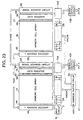
- FIG. 9 is a block diagram showing the structure of the serial access memory according to the third embodiment.
- the serial access memory shown in FIG. 9 is provided with an X address buffer circuit 60 having a function similar to that of each of the above described MSB control circuits 40A and 40B of the serial access memory according to the first embodiment, as an alternative to the MSB control circuits 40A and 40B.
- the X address buffer circuit 60 is supplied with an X address group XADD and a data transfer signal DT.
- the X address buffer circuit 60 converts the externally supplied X address group XADD into an internal X address group XADD', and supplies an internal X address group XADDA and an internal X address group XADDB to the respective X address decoders 2A and 2B.
- the X address buffer circuit 60 has a function to subtract only a predetermined value from the X address group XADDB so that the X address group XADDB is equal to the X address group XADDA during a data transfer cycle in which data are respectively transferred from memory cell arrays 1A and 1B to data registers 7A and 7B.
- a configuration of the X address buffer circuit 60 and specific configurations of its peripheral circuits will be described below with reference to FIGS. 10A and 10B.
- the X address buffer circuit 60 has a tristate inverter 118-1 electrically connected to the inverter 112 2n-1 so as to be supplied with a MSB (XADD 2n-1 ) of an X address XADD 2n-1 , a tristate inverter 118-2 similarly electrically connected to the inverter 116 2n-1 , and PMOSs 120-1 and 120-2 respectively electrically connected to the tristate inverters 118-1 and 118-2.
- the tristate inverters 118-1 and 118-2 are controlled by the data transfer signal DT supplied via an inverter 122.
- the operation of the X address buffer circuit 60 will be easily understood by reference to the description of the aforementioned MSB control circuit (see FIG. 4). That is, when the data transfer signal DT is in the "L" state, the X address buffer circuit 60 outputs the internal X address group XADD' based on the externally supplied X address group XADD.
- the X address group XADD' is made up of complementary addresses A 0 , A 0 to A 2n-1 , A 2n-1 .
- the X address buffer circuit 60 sets the complementary addresses A 2n-1 , A 2n-1 corresponding to the MSB of the internal X address group XADD' to the "H" state.
- the internal X address group XADD' output from the X address buffer circuit 60 is supplied to each of the address decoders 2A and 2B via a common data bus as shown in FIG. 10B.
- the X address buffer circuit when the above-described X address buffer circuit is employed in the serial access memory of the present invention, only the predetermined value is subtracted from the X address group XADDB upon transmission of data, so that the X address group XADDB becomes equal to the X address group XADDA.
- the X address group XADDA (A 0 to A n-1 ) and X address group XADDB (A n to A 2n-1 ) can be set on an arbitrary basis. That is, "n" may not be an integral multiple of 2, and hence the serial access memory can be widely used for various purposes.
- serial address circuits 8A and 8B supplied with the common serial address group SYADD consists of address pointers including shift registers operated in response to a common synchronizing clock, the same operations and effects as described above for the first embodiment can be obtained similarly for the third embodiment.
- a serial access memory according to a fourth embodiment of the present invention will next be described below.
- serial access memory according to the fourth embodiment of the present invention differs from that according to the third embodiment only in that independent serial address groups SYADDA and SYADDB are respectively input to the serial address circuits 8A and 8B.
- the serial access memory according to the fourth embodiment is operated in a manner substantially similar to that according to the third embodiment.
- the serial address groups SYADDA and SYADDB input to the corresponding serial address circuits 8A and 8B are independent, data stored in the data registers 7A and 7B at addresses different from each other can be output in serial form. That is, since data stored in the data registers 7A and 7B at respective different addresses can be selected, one pair of the data register 7A or 7B and the serial address circuit 8A or 8B can be independently operated even if theother pair of the data register 7A or 7B and the serial address circuit 8A or 8B has a defect. Further, since a serial address group is not applied in common to both serial address circuits, the serial address circuits 8A and 8B can obtain serial access to stored data asynchronously with respect to each other.
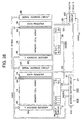
- a serial access memory according to a fifth embodiment of the present invention will now be described with reference to FIGS. 11 and 12.
- FIG. 11 is a block diagram schematically showing the structure of the serial access memory according to the fifth embodiment of the present invention. Elements common to those shown in FIG. 9 illustrating the third embodiment, are identified by common reference numerals.
- the serial access memory has an address buffer circuit 61 which performs the same function as the X address buffer circuit 60 which has been described above with respect to the third embodiment.
- the address buffer circuit 61 is externally supplied with an address group ADD, iand also supplied with a data transfer signal DT, a row address strobe signal RAS and a column address strobe signal CAS .
- the address buffer circuit 61 outputs internal X address groups XADDA and XADDB in the same manner as does the X address buffer circuit 60 of the third embodiment. Further, the address buffer circuit 61 functions to output an internal Y address group YADD, to be supplied to Y address decoders 5A and 5B.
- the address buffer circuit 61 has an address fetching function identical to that of a general-purpose DRAM, for time-divisionally taking in X and Y address groups from the address group ADD supplied from the same address terminal, based on the row address strobe signal RAS and the column address strobe signal CAS .
- FIG. 12 illustrates a specific circuit configuration of the address buffer circuit 61.
- the same elements of structure as those employed in the X address buffer circuit 60 shown in FIG. 10A are identified by the same reference numerals and their description will therefore be omitted.
- the address buffer circuit 61 has a gate circuit 130 externally supplied with the row address strobe signal RAS , input via an inverter 122, and with the address group ADD .
- the gate circuit 130 comprises NANDs 130 j -1, supplied with the row address strobe signal RAS and the external address group ADD, and inverters 130 j -2, respectively electrically connected between the outputs of the NANDs 130 j -1 and the inverters 110 i .
- the address buffer circuit 61 has a gate circuit 140 supplied with the column address strobe signal CAS via an inverter 124, and with the address group ADD.
- the gate circuit 140 is made up of NANDs 140 j -1, supplied with the column address strobe signal CAS and the external address group ADD, and inverters 140 i -2, respectively electrically connected between the outputs of the NAND's 140 i -1 and inverters 110' i .
- Components having the same functions as those of the components in the X address buffer circuit 60 are denoted by identical reference numerals with apostrophes ('), and their description will therefore be omitted.
- the address buffer circuit 61 in the serial access memory takes in the X address group on a time-sharing basis in response to the row address strobe signal RAS .
- the address buffer circuit 61 outputs the internal X address groups XADDA and XADDB in the same manner as the X address buffer circuit 60, described above with respect to the third embodiment, and supplies them to their corresponding X address decoders 2A and 2B.
- the address buffer circuit 61 brings the Y address group supplied on the time-sharing basis from the same address terminal.
- the address buffer circuit 61 outputs the internal Y address group YADD to each of the Y address decoders 5A and 5B.
- the access to memory cell arrays 1A and 1B is carried out in a manner similar to that carried out by the third embodiment.
- a serial access operation similar to that carried out by the third embodiment, is performed.
- the present fifth embodiment has an advantage in that since the externally-input address group ADD composed of the X and Y address groups can be brought from the same address terminal on a time-sharing basis due to the provision of the address buffer circuit 61, the number of terminals can be reduced.
- Each of serial address circuits 8A and 8B supplied with a common serial address group SYADD may be made up of an address pointer comprised of a register supplied with a common synchronizing clock.
- a serial access memory according to a sixth embodiment of the present invention will now be described below.
- serial access memory according to the sixth embodiment of the present invention is constructed in the same manner as the fifth embodimentexcept that independent serial address groups SYADDA and SYADDB are applied to the respective serial address circuits 8A and 8B.
- the serial access memory according to the sixth embodiment is basically operated in a manner substantially similar to that according to the fifth embodiment. Since the independent serial address groups SYADDA and SYADDB are input to the respective serial address circuits 8A and 8B, the data stored in the data registers 7A and 7B, at addresses different from each other, can be output serially. Therefore, the sizth embodiment of the serial access memory has not only substantially the same advantages as those obtained by that according to the fifth embodiment, but also the following advantages.
- one pair of the data register 7A or 7B and the serial address circuit 8A or 8B can be independently operated even if the other pair of the data register 7A or 7B and the serial address circuit 8A or 8B has a defect. Further, since the serial address groups SYADDA and SYADDB are different from each other, the serial address circuits 8A and 8B can also obtain serial access in asynchronism with each other, using these address groups.
- a serial access memory according to a seventh embodiment of the present invention will now be described below.
- FIG. 13 is a schematic block diagram showing the structure of the serial access memory according to the seventh embodiment of the present invention. Elements common to those shown in FIG. 1 illustrating the first embodiment are denoted by common reference numerals.
- first and second output-sequence converting circuits 70A and 70B are provided between a read data bus 9A and a serial output circuit 10A, and between a read data bus 9B and a serial output circuit 10B respectively.
- Each of the first and second output-sequence converting circuits 70A and 70B has a function to change the serial output sequence of read data transferred on each of the read data buses 9A and 9B based on address signals S 0 and S 1 provided for control of the serial output sequence.
- the circuits 70A and 70B provide the so-processed read data serially to the respective serial output circuits 10A and 10B.
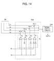
- FIG. 14 is a circuit diagram showing the configuration of the first output-sequence converting circuit 70A shown in FIG. 13.
- the second output-sequence converting circuit 70B is identical in circuit configuration to the first output-sequence converting circuit 70A.
- the first output-sequence converting circuit 70A is provided between the read data bus 9A (constructed, for example, in a 4-bit arrangement) and the serial output circuit 10A. Further, the first output-sequence converting circuit 70A has a decoder 71 comprised of NAND gates or the like, for decoding the address signals S 0 and S 1 , and NMOS's 72-1 to 72-4 controlled by decoded outputs P 1 to P 4 of the decoder 71 so as to connect the read data bus 9A to, and disconnect it from the serial output circuit 10A.
- a decoder 71 comprised of NAND gates or the like, for decoding the address signals S 0 and S 1 , and NMOS's 72-1 to 72-4 controlled by decoded outputs P 1 to P 4 of the decoder 71 so as to connect the read data bus 9A to, and disconnect it from the serial output circuit 10A.
- FIGS. 15A and 15B are timing diagrams for describing the operation of the output-sequence converting circuit 70A shown in FIG. 14. The operation of the serial access memory shown in FIGS. 13 and 14 will be described below with reference to FIGS. 15A and 15B.
- serial access memory is operated in a manner substantially similar to that according to the first embodiment but is different therefrom in the following aspects.
- each of the serial address circuits 8A and 8B decodes the serial address group SYADD in synchronism with a synchronizing control clock CLK. Based on the Result of the decoding, the serial address circuits 8A and 8B respectively transfer over the read data buses 9A and 9B the 4 bits of corresponding read data D 1 to D 4 which have been stored in the respective data registers 7A and 7B.
- each of the first and second output-sequence converting circuits 70A and 70B is activated such that the address signals S 0 and S 1 are decoded by the decoder 71 and the NMOSs 72-1 to 72-4 are respectively turned on or off by the resultant decoded outputs P 1 to P 4 . Therefore, the order or sequence for outputting the 4-bit read data D 1 to D 4 , which have been simultaneously transferred over each of the read data buses 9A and 9B, is changed.
- the read data thus subjected to the output-sequence change processing are output from each of output terminals OUTA and OUTB of the serial output circuits 10A and 10B.
- the seventh embodiment has advantages substantially similar to those obtained in the first embodiment and the following additional advantges.
- the sequence of serially outputting the read data can be controlled by each of the first and second output-sequence converting circuits 70A and 70B .
- the above processing to change output-sequence is effective, for example, in a case where the output sequence should be changed when RGB (red, green and blue) data corresponding to image data are respectively written into the corresponding memory cell arrays 1A and 1B in serial form and used in drawing an image on a liquid crystal screen or the like.
- each of the read data buses 9A and 9B is constructed in a 4-bit arrangement or unit.
- the read data buses 9A and 9B can be applied even to the case where the number of bits is 8, 16 or other desired number.
- Each of the serial address circuits 8A and 8B, supplied with the common serial address group SYADD, may comprise an address pointer including a register supplied with the common synchronizing clock in a manner similar to that described above with respect to the first embodiment.
- FIG. 16 shows an eighth embodiment of the present invention and illustrates one example of another structure of each output-sequence converting circuit described in the seventh embodiment. Elements common to those shown in the seventh embodiment are denoted by common reference numerals. In this case, a typical first output-sequence converting circuit 70A will be described below. A second output-sequence converting circuit 70B is substantially the same as the first output-sequence converting circuit 70A.
- the first output-sequence converting circuit 70A is provided with an address shift circuit 80, in addition to a decoder 71 and NMOS's 72-1 to 72-4 like those of circuit 70A shown in FIG. 14.
- the address shift circuit 80 is provided on the input side of the decoder 71 and serves as a circuit for inputting address signals S 0 and S 1 to the decoder 71.
- the address signals S0 and S1 control a serial read-data output sequence in response to an enable signal PIN for the input of an address sequence.
- the serial read-data output sequence is determined by the circuit 80 based on the address signals S 0 and S 1 .
- the circuit 80 supplies the result of its decision to the decoder 71 in synchronism with a synchronizing control clock CLK.
- the address shift circuit 80 comprises NMOS's 81 and 82 gate-controlled by the enable signal PIN so as to be supplied with the respective address signals S 0 and S 1 .
- Circuit 80 also includes an inverter 83 for inverting the enable signal PIN, NMOSs 84 and 85 gate-controlled by the output of the inverter 83, and four cascade-connected flip-flops 86-1 to 86-4 for shifting the input address signal S 0 in response to the synchronizing control clock CLK.
- Four cascade-connected flip-flops 87-1 to 87-4 are also included in the circuit 80 for shifting the input address signal S 1 in response to the synchronizing control clock CLK.
- the four cascade-connected flip-flops 86-1 to 86-4 are electrically connected to each other so that with the NMOS 84 they form a ring.
- the four cascade-connected flip-flops 87-1 to 87-4 are also electrically connected to each other so that a ring is formed with the NMOS 85.
- FIGS. 17A and 17B are timing diagrams for describing the operation of the output-sequence converting circuit shown in FIG. 16. The operation of the output-sequence converting circuit illustrated in FIG. 16 will be described below with reference to FIGS. 17A and 17B.
- the output-sequence converting circuit shown in FIG. 16 is basically operated in a manner substantially similar tothe above-described of operating the output-sequence converting circuit shown in FIG. 14.
- the NMOS's 81 and 82 are turned ON. Further, the enable signal PIN is inverted by the inverter 83 so that the NMOSs 84 and 85 are turned OFF.
- the address signals S 0 and S 1 are input to the respective flip-flops 86-1 and 87-1. Further, the address signals S 0 and S 1 are respectively shifted to the flip-flops 86-2 to 86-4 and 87-2 to 87-4 corresponding to the subsequent stages based on the synchronizing control clock CLK, to thereby determine a serial read-data output sequence.
- the determined sequence is supplied to the decoder 71 from the flip-flops 86-4 and 87-4, which correspond to the final stage.
- the decoder 71 decodes the determined serial output sequence as a four fit output P1 to P4 and turns ON or OFF the NMOS's 72-1 to 72-4 in accordance with this decoded output.
- the sequence for serially outputting 4 bit read data D 1 to D 4 which have been simultaneously transferred over each of read data buses 9A and 9B constructed in 4-bit units from each of data registers 7A and 7B, is changed by the NMOS's 72-1 to 72-4.
- the read data thus subjected to processing to change the output-sequence, are output from each of output terminals OUTA and OUTB of serial output circuits 10A and 10B.
- the NMOS's 81 and 82 are turned OFF. Further, the enable signal PIN is inverted by the inverter 83 so that the NMOS's 84 and 85 are turned ON. When the NMOS's 81 and 82 are turned OFF, the address signals S 0 and S 1 are prevented from being input to the NMOS's 81 and 82. When the NMOS's 84 and 85 are brought to the ON state, the flip-flops 86-1 to 86-4 are electrically connected to each other in a ring-like arrangement by the NMOS 84, so that the serial output sequence is held as it is.
- the flip-flops 87-1 to 87-4 are electrically connected to each other in a ring-like arrangement by the NMOS 85 so that the serial output sequence is held as it is. Thereafter, the above results are supplied to the decoder 71.
- the enable signal PIN may be set to the "H" level, so that the address signals S 0 and S 1 are input to the decoder 71.
- the serial access memory according to the eighth embodiment has the following advantage in addition to advantages similar to these obtained by the serial access memory according to the first embodiment.
- the sequence for outputting the read data D 1 to D 4 which have been simultaneously transferred over the read data buses 9A and 9B, can be controlled during the serial access operation. Therefore, the above processing to change the output sequence is effective, for example, in a case where the output sequence should be changed when RGB data corresponding to image data are serially written into the corresponding memory cell arrays 1A and 1B, and the data are to be used in drawing an image on a liquid crystal screen or the like.
- the output-sequence converting circuit shown in FIG. 14, which is employed in the seventh embodiment the address signals S 0 and S 1 for control of the serial output sequence should be supplied externally.
- the serial output sequence can be changed by simply inputting the enable signal PIN into the address shift circuit 80.
- each of the read data buses 9A and 9B is provided in a 4-bit arrangement or unit.
- the eighth embodiment can be applied even to read data buses provided in other bit units or arrangements such as 8-bit and 16-bit arrangements.
- Each of the serial address circuits 8A and 8B supplied with the common serial address group SYADD may cosist of an address pointer including a register supplied with a common synchronizing clock.
- FIG. 18 shows the ninth embodiment of the present invention and is a circuit diagram showing one example of a further structure of the first output-sequence converting circuit 70A which has been described in the description of the seventh embodiment. Elements common to those shown in FIGS. 14 and 16, which are employed in the seventh and eighth embodiments, are denoted by common reference numerals. Incidentally, the second output-sequence converting circuit 70B of this embodiment is substantially the same as the first output-sequence converting circuit 70A.
- the first output-sequence converting circuit 70A is basically similar to the output-sequence converting circuit employed in the eighth embodiment except as to the address shift circuit 80.
- the first output-sequence converting circuit 70A of the eighth embodiment is provided with four latch circuits 88-1 to 88-4, a four-stage type shift circuit 90 and four pairs of gate tristate inverters 89-1 to 89-8, for example, as an alternative to the address shift circuit 80.
- the four latch circuits 88-1 to 88-4 are of circuits which take in serial output-sequence decision addresses S 01 , S 11 , ..., S 04 , S 14 in response to an enable signal PIN for the input of address sequence.
- a decoder 71 is electrically connected to the outputs of the four latch circuits 88-1 to 88-4 via the four sets of tristate inverters 89-1 to 89-8.
- the shift circuit 90 consists of four flip-flops electrically connected to each other in a ring-like arrangement. Further, the shift circuit 90 has a function to perform a shift operation in response to a synchronizing control clock CLK, and successively to turn on and off the tristate inverters 89-1 to 89-8 two-by-two.
- the tristate inverters 89-1 to 89-8 perform normal signal inversion operations.
- the outputs of the shift circuit 90 are brought to the "L" level, each of the outputs of the tristate inverters 89-1 to 89-8 is brought into a high-impedance state.
- FIG. 19 is a timing diagram for explaining the operation of the output-sequence converting circuit shown in FIG. 18. The operation of the output-sequence converting circuit shown in FIG. 18 will now be described below with reference to FIG. 19.
- the latch circuits 88-1 to 88-4 take in the serial output-sequence decision addresses S 01 , S 11 , ..., S 04 , S 14 in response to the enable signal PIN.
- the shift circuit 90 is sequentially shifted in response to the synchronizing control clock CLK, so that the tristate inverters 89-1 to 89-8 are successively operated based on the outputs of the shift circuit 90.
- the outputs of the latch circuits 88-1 to 88-4 are inverted and the inverted outputs are supplied to the decoder 71.
- the decoder 71 decodes the inverted outputs from the tristate inverters 89-1 to 89-8, so as to produce decoded outputs P 1 to P 4 corresponding to 4 bits, thereby turning ON or OFF the four NMOS's 72-1 to 72-4 in accordance with the decoded outputs P 1 to P 4 .
- Similar processing is performed by the second output sequence converting circuit 70B.
- the serial output-sequence decision addresses S 01 , S 11 , ..., S 04 , S 14 are brought into the corresponding latch circuits 88-1 to 88-4 based on the enable signal PIN. Further, the serial output sequence of the read data D 1 to D 4 is changed in synchronism with the synchronizing control clock CLK based on the serial output-sequence decision addresses S 01 , S 11 , ..., S 04 , S 14 . Therefore, the ninth embodiment has the following advantage in addition to advantages substantially similar to those obtained by the seventh embodiment.
- serial output-sequence decision addresses S 01 , S 11 , ..., S 04 , S 14 are supplied externally, from the outside and the serial output sequence is changed based on such addresses, an output-sequence switching operation can be carried out at a high speed.
- the read data bus 9A shown in FIG. 18 is constructed in a 4-bit arrangement or unit, but may be arranged in a form which groups another desired number of bits.
- each of the serial address circuits 8A and 8B is supplied with a common serial address group SYADD, and may consist of an address pointer including a shift register supplied with a common synchronizing clock.
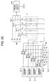
- FIG. 20 shows the tenth embodiment of the present invention and is a circuit diagram illustrating one example of a still further structure of the first output-sequence converting circuit 70A employed in the seventh embodiment. Elements common to those shown in the ninth embodiment are denoted by common reference numerals.
- the second output-sequence converting circuit 70B is of a circuit substantially the same as to the first output-sequence converting circuit 70A.
- the first output-sequence converting circuit 70A is basically similar to that in the ninth embodiment except that trimming circuits 91-1 to 91-4 replace the latch circuits 88-1 to 88-4. Trimming circuits 91-1 to 91-4 are used for determining the serial output sequence. Each trimming circuit has a function similar to that of the respective latch circuit it replaces.
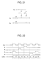
- FIG. 21 is a circuit diagram showing one example of the structure of each of the trimming circuits 91-1 to 91-4.
- Each of the trimming circuits 91-1 to 91-4 has fuses F1 and F2 used for determination of the serial output sequence.
- Each fuse has one end electrically connected to a power source potential VCC.
- the other end of fuse F1 is electrically connected to ground potentials VSS via resistor R1.
- the other end of fuse F2 is connected to ground potenrial VSS through a register R2.
- an address "01" is output.
- FIG. 22 is a timing diagram for describing the operation of the output-sequence converting circuit shown in FIG. 20. The operation of the output-sequence converting circuit illustrated in FIG. 20 will now be described below.
- the operation of the output-sequence converting circuit is basically identical substantially to that of the output-sequence converting circuit employed in the ninth embodiment. If serial output-sequence decision addresses are set in advance depending on the fuses F1 and F2 of the individual trimming circuits 91-1 to 91-4, then the output sequence of read data D 1 to D 4 is changed in synchronism with a synchronizing control clock CLK on the basis of the serial output-sequence decision addresses set by the trimming circuits 91-1 to 91-4. Thereafter, the read data thus subjected to processing to change the output sequence, are sequentially output from each of output terminals OUTA and OUTB of serial output circuits 10A and 10B.
- the present tenth embodiment has the following advantage in addition to advantages similar to those provided by the seventh embodiment. Since the serial output-sequence decision addresses can be set by the trimming circuit 91-1 to 91-4, it is unnecessary to input the serial output-sequence decision S 01 , S 11 , ..., S 04 , S 14 externally as in the ninth embodiment.
- the read data bus 9A may be set in a form having a desired number of bits other than 4 bits.
- each of the serial address circuits 8A and 8B is supplied with the common serial address group SYADD, and may cocsist of an address pointer including a shift register supplied with a common synchronizing clock.
- Serial access memories according to an eleventh embodiment of the present invention will now be described below.
- serial access memories are constructed in the following manner.
- Independent serial address groups SYADDA and SYADDB are employed (as an alternative to the common serial address group SYADD input to each of the serial address circuits 8A and 8B shown in FIG. 13), in any of the seventh, eighth, ninth and tenth embodiments (see FIGS. 14, 16, 18 and 20).
- the serial address group SYADDA is input to the serial address circuit 8A, whereas the remaining serial address group SYADDB is input to the serial address circuit 8B.
- the serial access memories according to the present embodiment is basically operated in a manner substantially similar to that of the above described operation of the serial access memories according to the seventh, eighth, ninth and tenth embodiments. Since, however, the serial address groups SYADDA and SYADDB are not in common, data stored in data registers 7A and 7B at different addresses respectively can be serially output. That is, since the data stored at different addresses in the the respective data registers 7A and 7B respectively can be selectively output, one pair of the data register 7A or 7B and the serial address circuit 8A or 8B can be independently operated even if the other pair of the data register 7A or 7B and the serial address circuit 8A or 8B has a defect. Further, since the serial address groups SYADDA and SYADDB are different from each other, the serial address circuits 8A and 8B can also obtain serial access in asynchronism with each other.
- FIG. 23 is a block diagram schematically showing the structure of the serial access memory according to the twelfth embodiment of the present invention. Elements common to those shown in FIG. 9, illustrating the third embodiment, and FIGS. 13 and 14, illustrating the seventh embodiment, are denoted by common reference numerals.
- the serial access memory according to the present embodiment corresponds to the serial access memory of FIG. 9 illustrating the third embodiment, wherein the first and second output-sequence converting circuits 70A and 70B in FIGS. 13 and 14, illustrating the seventh embodiment, are respectively connected between the read data buses 9A and 9B and the serial output circuits 10A and 10B.
- the serial access memory according to the present twelfth embodiment is operated in a manner substantially similar to the serial access memory according to the third embodiment (see FIG. 9). Since there are provided the first and second output-sequence converting circuits 70A and 70B of the configuration employed in the seventh embodiment, the sequence for serially outputting read data transferred over each of read data buses 9A and 9B from each of data registers 7A and 7B is changed, during the serial access operation, by each of the first and second output-sequence converting circuits 70A and 70B each of which is controlled by address signals S 0 and S 1 for control of the serial output sequence. Thereafter, the read data thus subjected to processing for changing the output sequence, are output from each of output terminals OUTA and OUTB of serial output circuits 10A and 10B.
- the present twelfth embodiment has advantages substantially similar to those obtained in the third embodiment. Further, since the serial output sequence can be controlled by each of the output-sequence converting circuits 70A and 70B, the above processing for changing the output sequence, is effective in, for example, a case where the output sequence should be changed when RGB data corresponding to image data are serially written into the corresponding memory cell arrays 1A and 1B and the data are to be used in drawing an image on a liquid crystal screen or the like.
- a serial access memory according to a thirteenth embodiment of the present invention will now be described below.
- FIG. 23 illustrating the twelfth embodiment, wherein the output-sequence converting circuits 70A and 70B are constructed according to the circuit diagram shown in FIG. 16, which illustrates the eighth embodiment.
- serial access memory according to the present twelfth embodiment is substantially similar to that according to the twelfth embodiment, except as to the operation of the output-sequence converting circuits 70A and 70B, which have a different circuit configuration. That is , in the present embodiment, data stored in data registers 7A and 7B are respectively transferred over read data buses 9A and 9B in serial form during serial access operation, so as to be supplied to the output-sequence converting circuits 70A and 70B.
- Each of the output-sequence converting circuits 70A and 70B receives address signals S 0 and S 1 for control of the serial output sequence, in response to an enable signal PIN, to thereby deermine a serial read-data output sequence in synchronism with a synchronizing control clock CLK. Thereafter, each of the output-sequence converting circuits 70A and 70B accordingly changes the sequence for serially outputting read data, and outputs the supplied read data in the determined sequence from each of output terminals OUTA and OUTB of serial output circuits 10A and 10B.
- the present embodiment has the advantages provided by the eighth embodiment as well as an advantage substantially similar to that provided by the twelfth embodiment.
- the present embodiment can be effectively applied to, for example, a case where the output sequence should be changed when RGB data corresponding to image data are serially written into the corresponding memory cell arrays 1A and 1B and used in drawing an image on a liquid crystal screen or the like.
- serial access memory according to the fourteenth embodiment of the present invention have a configuration like that illustrated in FIG. 23, but with output-sequence converting circuits 70A and 70B, each of which is represented by the circuit diagram shown in FIG. 18 (which illustrates the ninth embodiment).
- the basic operation of the serial access memory according to the fourteenth embodiment is substantially similar to that of the serial access memory according to the twelfth embodiment.
- the opeartion of the output-sequence converting circuits 70A and 70B are in accordance with the ninth embodiment. That is, when the output-sequence converting circuits 70A and 70B are respectively supplied with data stored in data registers 7A and 7B via read data buses 9A and 9B during serial access operation, each of the output-sequence converting circuits 70A and 70B receives serial output-sequence decision addresses S 01 , S 11 , ..., S 04 , S 14 , in response to an enable signal PIN.
- each of the output-sequence converting circuits 70A and 70B changes the serial read-data output sequence in synchronism with a synchronizing control clock CLK on the basis of the serial output-sequence decision addresses S 01 , S 11 , ..., S 04 , S 14 . Then, the read data, thus processed to change the output sequence, are output from the respective output terminals OUTA and OUTB of serial output circuits 10A and 10B. Therefore, the present embodiment can bring about the advantages obtained in the ninth and the twelfth embodiments.
- a serial access memory according to a fifteenth embodiment of the present invention will next be described below.
- the serial access memory according to the fifteenth embodiment of the present invention has a basic configuration like that of FIG. 23, illustrating the twelfth embodiment, but with output-sequence converting circuits 70A and 70B of the circuit configuration shown in FIG. 20 illustrating the tenth embodiment.
- the basic operation of the serial access memory according to the present fifteenth embodiment is substantially similar to that according to the twelfth embodiment.
- the operation of the output-sequence converting circuits 70A and 70B are in accordance with the tenth embodiment. That is, when data stored in each of data registers 7A and 7B is sent to the corresponding one of the output-sequence converting circuits 70A and 70B via each of read data buses 9A and 9B, during serial access operation, each of the output-sequence converting circuits 70A and 70B changes the serial read-data output sequence in synchronism with a synchronizing control clock CLK, on the basis of serial output-sequence decision addresses set by trimming circuits 91-1 to 91-4. Then, the read data thus processed to change the output sequence, are output from each of output terminals OUTA and OUTB of serial output circuits 10A and 10B Therefore, the present embodiment has the advantages provided by the tenth and twelfth embodiments.
- the serial access memory according to the sixteenth embodiment of the present invention has a basic configuration as shown in FIG. 23.
- independent serial address groups SYADDA and SYADDB are employed, as an alternative to the common serial address group SYADD, for separate input respectively the serial address circuit 8A andthe serial address circuit 8B, employed in the serial access memory shown in FIG. 23.
- This embodiment may be applied in cases in which the output-sequence converting circuits 70A and 70B are constructed according to any of the twelfth, thirteenth, fourteenth and fifteenth embodiments.
- the serial access memory according to the present sixteenth embodiment is operated basically in a manner substantially similar to the manner of operating the serial access memories according to the twelfth, thirteenth, fourteenth and fifteenth embodiments. Since, however, the serial address groups SYADDA and SYADDB are not used in common, data stored in data registers 7A and 7B at different addresses can be serially output. That is, since the data stored at the different addresses in the data registers 7A and 7B can be selectively output, one pair of the data register 7A or 7B and the serial address circuit 8A or 8B can be independently operated even if the other pair of the data register 7A or 7B and the serial address circuit 8A or 8B has a defect. Further, since the serial address groups SYADDA and SYADDB are different from each other, the serial address circuits 8A and 8B can also obtain serial access asynchronously.
- FIG. 24 is a block diagram schematically showing the structure of the serial access memory according to the seventeenth embodiment of the present invention. All elements common to those shown in FIG. 11 illustrating the fifth embodiment, except the output-sequenceconverting circuits 70A and 70B, are denoted by common reference numerals.
- serial access memory is constructed by modification of the fifth embodiment illustrated in FIG. 11, such that output-sequence converting circuits 70A and 70B are respectively connected between the read data buses 9A and 9B and the serial output circuits 10A and 10B.
- the serial access memory according to the present embodiment basically operates in a manner substantially similar to the serial access memory according to the fifth embodiment. However, since the output-sequence converting circuits 70A and 70B are provided, the serial access memory according to the present embodiment differs in its operation from that according to the fifth embodiment. That is, when data stored in data registers 7A and 7B are respectively transferred to the output-sequence converting circuits 70A and 70B via read data buses 9A and 9B during serial access operation, each of the output-sequence converting circuits 70A and 70B changes the serial read-data output sequence, based on the address signals S 0 and S 1 provided for control of the serial read-data output sequence. The circuits 70A and 70B then output the read data, in changed-sequence, from each of OUTA and OUTB of serial output circuits 10A and 10B.
- serial access memory has the following advantage in addition to advantages substantially similar to those provided by the fifth embodiment. Since output-sequence converting circuits 70A and 70B are provided, the serial output sequence can be controlled. Such serial output-sequence control is effective in, for example, a case where the output sequence should be changed when RGB data corresponding to image data are serially written into the corresponding memory cell arrays 1A and 1B and used in drawing an image on a liquid crystal screen or the like.
- a serial access memory according to an eighteenth embodiment of the present invention will now be described below.
- the eighteenth embodiment of the present invention has a construction like that of the serial access memory of FIG. 24 (illustrating the seventeenth embodiment), wherein the output-sequence converting circuits 70A and 70B each has the construction shown in FIG. 16 (which illustrates the eighth embodiment).
- the serial access memory according to the present embodiment basically operates in a manner substantially similar to that according to the seventeenth embodiment. Since, however, the output-sequence converting circuits 70A and 70B of the seventeenth and eighteenth embodiments differ in circuit configuration, the operation of the serial access memory of the eighteenth embodiment differs from the operation of the serial access memory according to the seventeenth embodiment.
- each of the output-sequence converting circuits 70A and 70B receives address signals S 0 and S 1 for control of the serial read-data output sequence, in response to an enable signal PIN, to thereby determine a serial read-data output sequence in synchronism with a synchronizing control clock CLK.
- each of the output-sequence converting circuits 70A and 70B changes the sequence for serially outputting read data, based on the result of the determination and outputs the read data in the changed sequence, from each of output terminals OUTA and OUTB of serial output circuits 10A and 10B.
- the present embodiment has the following advantage in addition to the advantages provided by the seventeenth embodiment.
- the serial read-data output sequence can be controlled by each of the output-sequence converting circuits 70A and 70B in the same manner as the eighth embodiment.
- output-sequence control is effective in, for example, a case where the output sequence should be changed when RGB data corresponding to image data are serially written into the corresponding memory cell arrays 1A and 1B and used in drawing an image on a liquid crystal screen or the like.
- the nineteenth embodiment of the present invention has a construction like that of the serial access memory of FIG. 24 (illustrating the seventeenth embodiment), wherein the output-sequence converting circuits 70A and 70B has the construction shown in FIG. 18 (which illustrates the ninth embodiment).
- the serial access memory according to the present nineteenth embodiment basically operates in a manner substantially similar to the operation of the serial access memory according to the seventeenth embodiment. Since, however, both output-sequence converting circuits 70A and 70B of the seventeenth and nineteenth embodiments differ in circuit configuration, the operation of the serial access memory according to the present embodiment differs from that of the seventeenth embodiment.
- each of the output-sequence converting circuits 70A and 70B of the nineteenth embodiment is activated so as to bring serial output-sequence decision addresses S 01 , S 11 , ..., S 04 , S 14 into their corresponding latch circuits 88-1 to 88-4, in response to an enable signal PIN.
- each of the output-sequence converting circuits 70A and 70B changes the serial read-data output sequence in synchronism with a synchronizing control clock CLK on the basis of the serial output-sequence decision addresses S 01 , S 11 , ..., S 04 , S 14 . Then, the read data, thus processed to change the output sequence, are output from the respective output terminals OUTA and OUTB of serial output circuits 10A and 10B. Therefore, the present embodiment can bring about the same advantages as those provided by the ninth and seventeenth embodiments.
- a serial access memory according to a twentieth embodiment of the present invention will now be described below.
- the twentieth embodiment of the present invention has a constructionlike that of the serial access memory of FIG. 24 (illustrating the seventeenth embodiment), wherein the output-sequence converting circuits 70A and 70B each has the construction shown in FIG. 20 (illustrating the tenth embodiment).
- the serial access memory according to the present twentieth embodiment basically operates in a manner substantially similar to the operation of the seventeenth embodiment. Since, however, both output-sequence converting circuits 70A and 70B of the present and seventeenth embodiments differ in circuit configuration, the opeation of the serial access memory according to the present embodiment differs from that of the seventeenth embodiment.
- each of the output-sequence converting circuits 70A and 70B changes the serial read-data output sequence in synchronism with a synchronizing control clock CLK, on the basis of serial output-sequence decision addresses set by the trimming circuits 91-1 to 91-4 shown in FIG. 21. Then, the read data thus processed to change the output-sequence change processing are output from each of output terminals OUTA and OUTB of serial output circuits 10A and 10B. Therefore, the present embodiment has the advantages provided the tenth and seventeenth embodiments.
- Serial access memory according to a twenty-first embodiment of the present invention will now be described below.
- serial access memories according to the twenty-first embodiment of the present invention have a basic construction as shown in FIG. 24.
- independent serial address groups SYADDA and SYADDB are employed, as an alternative to the common serial address group SYADD for separative input respectively to the serial address circuit 8A and the serial address circuit 8B, employed in the serial access memory shown in FIG. 24.
- This embodiment may be applied in cases in which the output-sequence converting circuits 7A and 7B are constructed according to the seventeenth, eighteenth, nineteenth and twentieth embodiments.
- the serial access memories according to the present embodiment basically operates in a manner substantially similar to the serial access memories according to the seventeenth, eighteenth, nineteenth and twentieth embodiments. Since, however, the serial address groups SYADDA and SYADDB are in common, data stored in data registers 7A and 7B at different addresses can be output serially. That is, since the data stored at the different addresses in the respective data registers 7A and 7B can be selectively output, one pair of the data register 7A or 7B and the serial address circuits 8A or 8B can be independently operated even if the othe pair of the data register 7A or 7B and the serial address circuit 8A or 8B has a defect. Further, since the serial address groups SYADDA and SYADDB are different from each other, the serial address circuits 8A and 8B can also obtain serial access asynchronously.
- FIG. 25 is a block diagram schematically showing the structure of the serial access memory according to the twenty-second embodiment of the present invention. Elements common to those shown in FIG. 1 illustrating the first embodiment, are denoted by common reference numerals.
- the serial access memory according to the twenty-second embodiment differs from that according to the first embodiment in that a common output circuit 100 is provided as an alternative to the serial output circuits 10A and 10B shown in FIG. 1.
- the common output circuit 100 has an input electrically connected to read data buses 9A and 9B and an output electrically connected to two output terminals DOUTA and DOUTB. Further, the common output circuit 100 has a function to provide the output thereof at either one port or two ports in response to an output mode conversion signal TFT and a maximum X address XADD max (MSB).
- FIG. 26 is a circuit diagram showing the configuration of the output circuit 100 shown in FIG. 25.
- the maximum X address XADD max is input to a tristate inverter 101, the output of which is electrically connected to one of the inputs of a NOR gate 107.
- a read data bus 9B is electrically connected to the respective inputs of tristate inverters 102 and 104, whereas a read data bus 9A is electrically connected to the respective inputs of tristate inverters 103 and 105.
- the output mode conversion signal TFT and the output of the NOR gate 107 are input to the corresponding inputs of a NOR gate 106.
- the tristate inverter 102 is switched or turned on and off in response to the output of the NOR gate 106.
- the output mode conversion signal TFT and the output of the tristate inverter 101 are input to corresponding inputs of a NOR gate 107.
- the tristate inverter 103 is operably controlled in response to the output of the NOR gate 107.
- Each of the tristate inverters 104 and 105 is operably controlled in response to the output mode conversion signal TFT .
- the outputs of the tristate inverters 102 and 105 are electrically connected in common to an output terminal DOUTA.
- the output of the tristate inverter 104 is electrically connected to an output terminal OUTB.
- the serial access memory according to the present twenty-second embodiment basically operates in a manner substantially similar to that according to the first embodiment. However, since the present embodiment is provided with the common output circuit 100, its output operation differs from that of the first embodiment. That is, refering to FIG. 26, when the output mode conversion signal TFT is in an "L" state, the NOR gates 106 and 107 are enabled and the outputs of the tristate inverters 104 and 105 are brought into a high-impedance state. When the NOR gates 106 and 107 are enabled, the outputs of the NOR gates 106 and 107 vary according to the maximum X address XADD max .
- the tristate inverters 102 and 103 are turned on and off in response to the outputs of the NOR gates 106 and 107.
- the output mode conversion signal TFT is in an "H” state
- the NOR gates 106 and 107 are disabled so that the outputs thereof are brought into the "L” state.
- the outputs of the tristate inverters 102 and 103 are brought into a high-impedance state and each of the tristate inverters 104 and 105 is turned on so as to perform a normal inversion operation.
- a serial read output on either one of the read data buses 9A and 9B can be output from the output terminal DOUTA based on the maximum X address XADD max as if a two-port output type device could be activated in the form of one port by controlling the level of the output mode conversion signal TFT .
- the output terminal DOUTB corresponding to the other port is brought into a high-impedance state.
- serial output operations can be effected even in the case of a serial access memory of such a type that the serial outputs are respectively generated from the same X addresses (the same relative locations) relatively identical to each other in the memory cell arrays 1A and 1B, as has been described with respect to the first embodiment.
- the serial access memory has the following advantages due to the provision of the common output circuit 100, in addition to advantages substantially similar to those provided by the first embodiment.
- Either one of the input serial read outputs can be output from the output terminals DOUTA based on the maximum X address XADD max , as though the two-port output type device could be activated in the form of one port, by controlling the level of the output mode conversion signal TFT .
- the output terminal DOUTB corresponding to the other port is brought into the high-impedance state.
- the output circuit 100 can be freely set to operate as either one port or two ports, depending on the purpose, by simply controlling the level of the output mode conversion signal TFT . Therefore, the serial access memory is easy to put into free use and can be widely used for various purposes.
- the serial access memory can be made inexpensive from the standpoint of its manufacture.
- the value of the output mode conversion signal TFT may be decided by an externally-input type control system, or may be determined by laser fuse trimming, an option mask or the like, in a final manufacturing step.
- serial access memory has a basic construction as shown in FIG. 26.
- independent serial address groups SYADDA and SYADDB are employed, as an alternative to the common serial address group SYADD, for separate input respectively to the serial address circuit 8A and the serial address circuit 8B, employed in the serial access memory of FIG. 25.
- the serial access memory according to the present embodiment basically operates in a manner substantially similar to the serial access memory according to the twenty-second embodiment. However, since the serial address groups SYADDA and SYADDB are not in common, data stored at different addresses in the respective data registers 7A and 7B, can be output serially. Thus, the present embodiment has the advantages obtained in the second and twenty-second embodiments.
- FIG. 27 is a block diagram schematically showing the serial access memory according to the twenty-fourth embodiment of the present invention. Elements common to those in FIG. 9 illustrating the third embodiment, are identified by common reference numerals.
- the output circuit 100 of FIG. 26 illustrating the twenty-second embodiment is electrically connected to read data buses 9A and 9B as an alternative to the serial output circuits 10A and 10B shown in FIG. 9 illustrating the third embodiment.
- the serial access memory according to the present twenty-fourth embodiment basically operates in a manner substantially similar to that according to the third embodiment.
- the output circuit 100 is electrically connected to the read data buses 9A and 9B. Therefore, a serial read output on either one of the read data buses 9A and 9B can be output from an output terminal DOUTA based on the maximum X address XADD max , in a manner similar to output operations of the twenty-second embodiment, as if the output circuit 100 of a two-port output type could be activated in the form of one port, by controlling the level of an output mode conversion signal TFT . Accordingly, the present embodiment has both the above-described advantages provided by the third embodiment, and the above-described advantages provided by the output circuit in FIG. 27 illustrating the twenty-second embodiment.
- serial access memory has a basic construction as shown in FIG. 27.
- independent serial address groups SYADDA and SYADDB are employed, as an alternative to the common serial address group SYADD for separative input respectively to the serial address circuit 8A and the serial address circuit 8B.
- the serial access memory according to the present embodiment basically operates in a manner substantially similar to the serial access memory according to the fourth embodiment.
- the output circuit 100 is provided in place of output circuits 10A and 10B, a serial read output on either one of read data buses 9A and 9B can be output from an output terminal DOUTA based on the maximum X address XADD max in a manner similar to the twenty-fourth embodiment. That is, the two-output port type output circuit 100 can be activated in the form of one port, by controlling the level of the output mode conversion signal TFT . Accordingly, the present embodiment has the advantages provided by the fourth embodiment and that provided by the output circuit of the twenty-second embodiment.
- FIG. 28 is a block diagram schematically illustrating the structure of the serial access memory according to the twenty-sixth embodiment of the present invention. Elements common to those shown in FIG. 11 illustrating the fifth embodiment and FIG. 26 illustrating the twenty-second embodiment, are identified by common reference numerals.
- the output circuit 100 shown in FIG. 26, illustrating the twenty-second embodiment is provided as an alternative to the serial output circuits 10A and 10B, shown in FIG. 11 illustrating the fifth embodiment. Further, the output circuit 100 is electrically connected to both read data buses 9A and 9B.
- the serial access memory according to the present embodiment is activated in basically the same manner as is that according to the fifth embodiment. Since the output circuit 100 is provided in place of the serial output circuits 10A and 10B, a serial read output on either one of the read data buses 9A and 9B can be output from an output terminal DOUTA based on the maximum X address XADD max as if the output circuit 100 of a two-port output type could be activated in the form of one port by controlling the level of an output mode conversion signal TFT. Such operation is possible even in the case of a serial access memory of such a type that serial outputs are respectively generated from the same X addresses (the same relative locations) in the memory cell arrays 1A and 1B.
- the present embodiment has not only advantages substantially similar to those provided by the fifth embodiment, but also the advantage obtained in the twenty-second embodiment, due to the provision of the common output circuit 100.
- the serial access memory according to the twenty-seventh embodiment of the present invention has a basic construction as shown in FIG. 28.
- independent serial address groups SYADDA and SYADDB are employed as an alternative to the common serial address group SYADD input to each of the serial address circuits 8A and 8B, in the serial access memory of FIG. 28 illustrating the twenty-sixth embodiment.
- the twenty-seventh embodiment may also be viewed as a modification of the sixth embodiment wherein the output circuit 100 of FIG. 26 replace the separate output circuits 10A and 10B.
- serial access memory data stored at different addresses respectively in data registers 7A and 7B, can be output serially, since the serial address groups SYADD and SYADDB are different from each other. Since there is also provided a common output circuit 100, a serial read output on either one of read data buses 9A and 9B can be output from an output terminal DOUTA as if the output circuit 100, of the two-port output type, could be activated in the form of one port, by controlling the level of an output mode conversion signal TFT . Accordingly, the present embodiment can provide the same advantages provided by the sixth and twenty-second embodiments.
- FIG. 29 is a block diagram schematically showing the structure of the serial access memory according to the twenty-eighth embodiment of the present invention. Elements common to those shown in FIGS. 13 and 14 illustrating the seventh embodiment and FIG. 26 illustrating the twenty-second embodiment, are denoted by common reference numerals.
- the output circuit 100 in FIG. 26, illustrating the twenty-second embodiment is provided as an alternative to the serial output circuits 10A and 10B shown in FIG. 13, illustrating the seventh embodiment
- the output circuit 100 is electrically connected to read data buses 9A and 9B.
- output-sequence converting circuits 70A and 70B in the serial access memory in a manner similar to the seventh embodiment, the order or sequence for serially outputting read data on the read data buses 9A and 9B can be changed, and the read data thus processed can be output in the changed sequence.
- a common output circuit 100 is provided in a manner similar to the twenty-second embodiment, the serial read data on either one of the read data buses 9A and 9B can be output from an output terminal DOUTA based on the maximum X address XADD max, as if the output circuit 100, of a two-port output type, could be activated in the form of one port, by controlling the level of an output mode conversion signal TFT .
- the present embodiment can bring about the same advantages provided by the seventh and twenty-second embodiments.
- the serial access memory according to the twenty-ninth embodiment of the present invention has a basic construction according to the circuit diagram of FIG. 29, wherein each of the output-sequence converting circuits 70A and 70B has a constructionaccording to the circuit shown in FIG. 16 illustrating the eighth embodiment and the common output circuit 100 has the construction shown in FIG. 26 illustrating the twenty-second embodiment. Therefore, the serial access memory can bring about operations and effects similar to those obtained by the output-sequence converting circuits 70A and 70B employed in the eighth embodiment and to those obtained by the output circuit 100 in FIG. 26 illustrating the twenty-second embodiment.
- the serial access memory according to the thirtieth embodiment of the present invention has a basic construction according to the circuit diagram of FIG. 29, wherein each of the output-sequence converting circuits 70A and 70B has a construction according to the circuit shown in FIG. 18 illustrating the ninth embodiment, and the common output circuit 100 has the construction shown in FIG. 26 illustrating the twenty-second embodiment. Therefore, the present embodiment can bring about operations and effects similar to those obtained by the output-sequence converting circuits 70A and 70B employed in the ninth embodiment and the common output circuit 100 in FIG. 26 illustrating the twenty-second embodiment.
- the serial access memory according to the thirty-first embodiment of the present invention has a construction according to the circuit diagram of FIG. 29, wherein each of the output-sequence converting circuits 70A and 70B has a construction according to the circuit shown in FIG. 20 illustrating the tenth embodiment and the common output circuit 100 has the construction shown in FIG. 26 illustrating the twenty-second embodiment. Therefore, the present embodiment can bring about operations and effects similar to those obtained by the output-sequence converting circuits 70A and 70B employed in the tenth embodiment and the output circuit 100 in FIG. 26 illustrating the twenty-second embodiment.
- Serial access memories according to a thirty-second embodiment of the present invention will now be described below.
- serial access memories according to the thirty-second embodiment of the present invention have a basic construction as shown in FIG. 29.
- independent serial address groups SYADDA and SYADDB are employed, as an alternative to the common serial address group SYADD, for separate input to the respective serial address circuits 8A and 8B shown in FIG. 29, in any of the twenty-eighth, twenty-ninth, thirtieth and thirty-first embodiments.
- the serial address groups SYADDA and SYADDB are different from each other, as in the eleventh embodiment. Therefore, data stored in data registers 7A and 7B at different addresses can be serially output. Further, a common output circuit 100 is provided on the output sides of output-sequence converting circuits 70A and 70B, in a manner similar to each of the twenty-eighth to thirty-first embodiments. Therefore, a serial read output on either one of read data buses 9A and 9B can be output from one output terminal DOUTA, as if the output circuit 100 of a two-port output type could be activated in the form of one port, by controlling the level of an output mode conversion signal TFT . Accordingly, the present embodiment can bring about the advantage provided by the eleventh embodiment and the advantages provided by the twenty-eighth to thirty-first embodiments.
- FIG. 30 is a block diagram schematically showing the structure of the serial access memory according to the thirty-third embodiment of the present invention. Elements common to those in FIG. 23, illustrating the twelfth embodiment, and those in FIG. 26, illustrating the twenty-second embodiment, are denoted by common reference numerals.
- serial access memory is obtained by substituting the common output circuit 100 of FIG. 26 for the serial output circuits 10A and 10B, in FIG. 23 illustrating the twelfth embodiment illustrated in FIG. 23,with the output circuit 100 electrically connected to the outputs of output-sequence converting circuits 70A and 70B.
- the serial access memory according to the present embodiment is activated in basically the same manner that the twelfth embodiment is activated.
- the common output circuit 100 since the common output circuit 100 is provided, the serial access memory of the present embodiment operates differently than the twelfth embodiment. That is, the common output circuit 100 has a function to receive therein an output mode conversion signal TFT , and a maximum X address XADD max brought into an "L" state when an X address decoder 2A is selected, and an "H" state when an X address decoder 2B is selected.
- the output circuit 100 outputs serial data from the output-sequence converting circuits 70A and 70B to output terminals DOUTA and DOUTB respectively.
- a serially read output on either one of read data buses 9A and 9B can be output from the output terminal DOUTA based on the maximum X address XADD max , as if the output circuit 100 of a two-port output type could be activated as one port by controlling the level of the output mode conversion signal TFT .
- the output terminal DOUTB corresponding to the other port is brought into a high-impedance state.
- such as output operation can be effected even in the case of a serial access memory of such a type that serial outputs are respectively generated from the same X addresses in the respective memory cell arrays 1A and 1B, as has been described above with regard to the twelfth embodiment.
- the present embodiment has advantages substantially similar to those provided by the twelfth embodiment. Further, since there is provided the common output circuit 100, the present embodiment can bring about the following advantage in a manner similar to the twenty-second embodiment.
- the output circuit 100 corresponding to the identical device can be freely set to output data from either one port or two ports, depending on the purpose, by simply controlling the level of the output mode conversion signal TFT . Therefore, the serial access memory has advantages of increased convenience and breadth of use.
- a serial access memory provides output-sequence converting circuits having the construction shown in FIG. 16, illustrating the eighthembodiment, as circuits 10A and 10B in the serial access memory of FIG. 30 illustrating the thirty-third embodiment. Therefore, the present embodiment performs operations and provides effects, substantially similar to those provided by the eighth and thirty-third embodiments.
- a serial access memory provides output-sequence converting circuits having the consruction shown in FIG. 18, illustrating the ninth embodiment, as circuits 70A and 70B of the serial access memory of FIG. 30, illustrating the thirty-third embodiment. Therefore, the present embodiment performs operations and provides effects, substantially similar to those obtained in the ninth and thirty-third embodiments.
- a serial access memory provides output-sequence converting circuits having the constructionshown in FIG. 20, illustrating the tenth embodiment, as circuits 70A and 70B of the serial access memory of FIG. 30, illustrating the thirty-third embodiment. Therefore, the present embodiment performs operations and provides effects substantially similar to those obtained in the tenth and thirty-third embodiments.
- Serial access memories according to a thirty-seventh embodiment of the present invention will now be described below.
- serial access memories according to the present thirty-seventh embodiment of the present invention have a basic constructionas shown in FIG. 30.
- independent serial address groups SYADDA and SYADDB are used in place of the common serial address group SYADD, for separative input to the respective serial address circuits 8A and 8B shown in FIG. 30, in any of the thirty-third, thirty-fourth, thirty-fifth and thirty-sixth embodiments.
- the serial address groups SYADDA and SYADDB are different from each other, data stored at different addresses in the respective data registers 7A and 7B, can be serially output in a manner similar to the manner in which data is output by the sixteenth embodiment. Accordingly, the present embodiment can bring about the advantages provided by the sixteenth embodiment and the advantages provided by the thirty-third, thirty-fourth, thirty-fifth, or thirty-sixth embodiment.
- FIG. 31 is a block diagram schematically showing the structure of the serial access memory according to the thirty-eighth embodiment of the present invention. Elements common to those shown in FIG. 24, illustrating the seventeenth embodiment, and FIG. 25, illustrating the twenty-second embodiment, are denoted by common reference numerals.
- the common output circuit 100 in FIG. 25, illustrating the twenty-second embodiment is provided as an alternative to the serial output circuits 8A and 8B in FIG. 24, illustrating the seventeenth embodiment.
- the serial access memory according to the present embodiment is operated in a manner basically similar to the seventeenth embodiment. Since, however, the common output circuit 100 in FIG. 25, illustrating the twenty-second embodiment, is provided in place of the serial output circuits 10A and 10B, the serial access memory of this embodiment operates differently than the seventeenth embodiment. That is, the common output circuit 100 has a function to receive therein an output mode conversion signal TFT , and a maximum X address XADD max , which takes on an "L" state when an X address decoder 2A is selected and an "H" state when an X address decoder 2B is selected. The circuit 100 outputs serially read outputs respectively on read data buses 9A and 9B, to the output terminals DOUTA and DOUTB.
- the serially read output on either one of the read data buses 9A and 9B can be output from the output terminal DOUTA, based on the maximum X address XADD max , as if the output circuit 100 of a two-port output type could be activated in the form of one port, by controlling the level of the output mode conversion signal TFT .
- the output terminal DOUTB corresponding to the other port, is brought into a high-impedance state.
- the present embodiment can bring about the advantages obtained in the seventeenth and twenty-second embodiments.
- a serial access memory provides the output-sequence converting circuits having the construction shown in FIG. 16, illustrating the eighthembodiment, as circuits 70A and 70B of the serial access memory of FIG. 31, illustrating the thirty-eighth embodiment. Therefore, the present embodiment can bring about operations and effects substantially similar to those obtained in the eighth and thirty-eighth embodiments.
- a serial access memory provides output-sequence converting circuits having the construction shown in FIG. 18, illustrating the ninth embodiment, as circuits 70A and 70B of the serial access memory of FIG. 31, illustrating the thirty-eighth embodiment. Therefore, the present embodiment can bring about operations and effects substantially similar to those obtained in the ninth and thirty-eighth embodiments.
- a serial access memory according to a torty-first embodiment of the present invention provides output-sequence converting circuits having the construction shown in FIG. 20, illustrating the tenth embodiment, as circuits 70A and 70B of the serial accessmemory of FIG. 31, illustrating the thirty-eighth embodiment is comprised of the circuit in FIG. 20 illustrating the tenth embodiment. Therefore, the present embodiment can bring about operations and effects substantially similar to those obtained in the tenth and thirty-eighth embodiments.
- Serial access memories according to a forty-second embodiment of the present invention will now be described below.
- serial access memories according to the forty-second embodiment of the present invention have a basic construction as shown in FIG. 31.
- independent serial address groups SYADDA and SYADDB are used as an alternative to the common serial address group SYADD, for separative input to the respective serial address circuits 8A and 8B shown in FIG. 31, in any of the thirty-eighth, thirty-ninth, fortieth and forty-first embodiments.
- data stored at different addresses in the respective data registers 7A and 7B can be serially output in a manner similar to the manner in which data is output by the twenty-first embodiment, because the serial address groups SYADDA and SYADDB are different from each other.
- the present embodiment can bring about the operations and advantageous effects obtained in the twenty-first embodiment as well as operations and advantageous effects similar to those obtained in each of the thirty-eighth, thirty-ninth, or fortieth embodiments or those obtained in the forty-first embodiment.
Description
- This invention relates to a semiconductor memory, and particularly to a serial access memory that can be used in image processing and operated at a high speed.
- A serial access memory has been widely used for image processing in personal computers, word processors and the like. The serial access memory employed in image processing needs a high image-drawing speed. To meet such a demand, a device is normally used wherein a serial access memory is electrically connected to a general-purpose dynamic random access memory (hereinafter called a "DRAM"). This type of device writes data into the DRAM and thereafter reads data corresponding to a desired row, one row at a time. Then, the read data are transferred to the serial access memory, from which the data are serially read.
- This type of serial access memory has been disclosed in Japanese Patent Application Laid-Open Publication Nos. 2-105388 (Laid-Open Date: April 17, 1990) and 3-76091 (Laid-Open Date: April 2, 1991).
- US-A-4,450,538 discloses an address accessed memory device having parallel to serial conversion. Therein, a memory device is provided with first and second memories. Two groups of data are loaded into the first and second memories, through a data buffer register. The same address information is applied to the first and second memories and the information is read out from the first and second memories. The two groups of the data read out in parallel are applied to a data multiplexer which in turn converts the parallel information into the serial one.
- EP-A-0 174 845 discloses a semiconductor memory device. Therein, the semiconductor memory device can continuously read or store a plurality of data therefrom or therein. The semiconductor memory device includes a memory unit having a plurality of memory cells, the memory cells being arranged in a matrix having rows and columns, and a reading storing circuit. The reading storing circuit can read or store data from or into the memory cell at an address corresponding to an address signal received therein in response to the reception of first and second control signals, respectively. The reading storing circuit also can consecutively read or store data from or into the memory cell at another address subsequent to the address read or stored at the last time in response to the reception of the second control signal. Such a device can therefore have improved access time for continuous accessing of a plurality of data.
- It is an object of the present invention to provide a serial access memory which can be operated at a high speed.
- It is another object of the present invention to provide a serial access memory which is capable of easily producing memory maps in memory cells and makes it unnecessary to provide externally-mounted elements such as a multiplexer, etc., and particularly to provide a serial access memory applicable to a Super Twined Nematic (STN) type liquid crystal display (LCD) which is employed in office automation (OA) devices such as a laptop personal computer, a word processor, etc.
- The present invention is defined in
independent claim 1. Preferred embodiments are disclosed in the dependent claims. - In order to achieve the above objects, the present invention provides a serial access memory comprising first and second memory cell arrays, which memory is provided with a control circuit for controlling the Most Significant Bit (MSB) of an addess supplied to each of the first and second memory cell arrays. That is, a MSB control circuit is provided which is capable of making the MSB of each address appear invalid when data is transferred from each memory cell array. Owing to the provision of the MSB control circuit, the operations of circuits in the first memory cell array become identical to those of circuits in the second memory cell array.
- Further, when the serial access memory of the present invention is applied to the STN type LCD, a display device can be materialized which is capable of easily producing memory maps in memory cells and making it unnecessary to provide externally-mounted elements such as a multiplexer, etc.
- While the specification concludes with claims particularly pointing out and distinctly claiming the subject matter which is regarded as the invention, it is believed that the invention, and the objects, features and advantages thereof will be better understood from the following description taken in connection with the accompanying drawings in which:
- FIG. 1 is a fragmentary block diagram showing the structure of a serial access memory according to a first embodiment of the present invention;
- FIG. 2 is a fragmentary block diagram showing the serial access memory of FIG. 1 in detail;
- FIG. 3 is a schematic block diagram showing the structure of a Most Significant Bit (MSB) control circuit shown in FIG. 1;
- FIG. 4 is a block diagram illustrating the specific structures of the MSB control circuit shown in FIG. 3 and its peripheral circuits;
- FIG. 5 is a partial timing chart for describing a portion of the operation of the serial access memory according to the present invention;
- FIGS. 6(A) and 6(B) are explanatory views illustrating a typical serial access operation of the serial access memory according to the present invention;
- FIGS. 7(A) and 7(B) are respectively explanatory views illustrating a typical random access operation of the serial access memory according to the present invention;
- FIG. 8 is a block diagram showing one example in which the serial access memory according to the present invention is applied to a Super Twined Nematic (STN) type Liquid Crystal Display (LCD);
- FIG. 9 is a fragmentary block diagram showing the structure of a serial access memory according to a third embodiment of the present invention;
- FIGS. 10(A) and 10(B) are fragmentary block diagrams showing the specific structures of the X address buffer circuit shown in FIG. 9 and its peripheral circuits;
- FIG. 11 is a fragmentary block diagram showing the structure of a serial access memory according to a fifth embodiment of the present invention;
- FIG. 12 is a fragmentary block diagram illustrating a specific configuration of an address buffer circuit shown in FIG. 11;
- FIG. 13 is a fragmentary block diagram showing the structure of a serial access memory according to a seventh embodiment of the present invention;
- FIG. 14 is a block diagram illustrating the structure of an output-sequence converting circuit shown in FIG. 13;
- FIGS. 15(A) and 15(B) are respective partial timing charts for describing the operation of the output-sequence converting circuit shown in FIG. 14;
- FIG. 16 is a block diagram illustrating the structure of an output-sequence converting circuit employed in a serial access memory according to an eighth embodiment of the present invention;
- FIGS. 17(A) and 17(B) are respectively partial timing charts for describing the operation of the output-sequence converting circuit shown in FIG. 16;
- FIG. 18 is a block diagram depicting the structure of an output-sequence converting circuit employed in a serial access memory according to a ninth embodiment of the present invention;
- FIG. 19 is a partial timing chart for explaining the operation of the output-sequence converting circuit shown in FIG. 18;
- FIG. 20 is a block diagram showing the structure of an output-sequence converting circuit employed in a serial access memory according to a tenth embodiment of the present invention;
- FIG. 21 is a block diagram showing the configuration of a trimming circuit which is a component of the output-sequence converting circuit shown in FIG. 20;
- FIG. 22 is a partial timing chart for describing the operation of the output-sequence converting circuit shown in FIG. 20;
- FIG. 23 is a fragmentary block diagram showing the structure of a serial access memory according to a twelfth embodiment of the present invention;
- FIG. 24 is a fragmentary block diagram illustrating the structure of a serial access memory according to a seventeenth embodiment of the present invention;
- FIG. 25 is a fragmentary block diagram depicting the structure of a serial access memory according to a twenty-second embodiment of the present invention;
- FIG. 26 is a block diagram specifically showing the configuration of an output circuit shown in FIG. 25;
- FIG. 27 is a fragmentary block diagram illustrating the structure of a serial access memory according to a twenty-fourth embodiment of the present invention;
- FIG. 28 is a block diagram depicting the structure of a serial access memory according to a twenty-sixth embodiment of the present invention;
- FIG. 29 is a block diagram showing the structure of a serial access memory according to a twenty-eighth embodiment of the present invention;
- FIG. 30 is a block diagram illustrating the structure of a serial access memory according to a thirty-third embodiment of the present invention; and
- FIG. 31 is a block diagram showing the structure of a serial access memory according to a thirty-eighth embodiment of the present invention.
-
- Preferred embodiments of the present invention will hereinafter be described with reference to the accompanying drawings. Common elements employed in the respective embodiments are identified by like reference numerals. In the respective embodiments, memory control signal generating circuits and the like, which are not directly concerned with a basic operation of the present invention, are omitted to facilitate understanding of the description.
- A serial access memory according to a first embodiment of the present invention will first be described with reference to FIGS. 1 and 2. FIG. 1 is a block diagram showing the structure of the serial access memory of the present invention. FIG. 2 is a block diagram illustrating, in detail, the structure of a principal part of the serial access memory shown in FIG. 1. Elements shown in FIG. 2, which are common to those shown in FIG. 1 are identified by the same reference numerals as those employed in FIG. 1.
- The serial access memory according to the present embodiment has a first
memory cell array 1A and a secondmemory cell array 1B. Thememory cell arrays BLai which intersect these word lines WLai and WLaj. Memory cells Qkj (k = 1 to m, i = 1 to n), each comprised of a transistor and a capacitor, are respectively electrically connected to points where the word lines WLai intersect the bit lines BLai. Further, the memory cells Qki are arranged in row and column directions. Similarly, memory cellsQki (k = 1 to m, i = 1 to n), each comprised of a transistor and a capacitor, are respectively electrically connected to points where the word lines WLaj intersect the bit lines BLai respectively. The respective bit line pairs BLai andBLai are respectively electrically connected to sense amplifiers SAi (i = 1 to n).X address decoders memory cell arrays X address decoder 2A is electrically connected to the word lines WLai and WLaj of thearray 1A. Further, theX address decoder 2A has a function to decode 0th to N-1th X addresses XADDAa (binary values 0 to N-1) of an ordered X address group XADD and selecting a desired column from thememory cell array 1A. TheX address decoder 2B is electrically connected to the word lines WLai and WLaj of thearray 1B. Further, theX address decoder 2B has a function to decode Nth to 2N-1th X addresses XADDBa (binary values N to 2N-1) of the X address group XADD and selecting a desired column from thememory cell array 1B. - An
input circuit 3 is of a circuit for inputting write data inputted from an input terminal IN to thememory arrays write data buses -
Y address decoders trai (i = 1 to n). The transistor pairs trai andtrai (i = 1 to n) of thedecoders write data buses BLai respectively of thememory cell arrays unit Y decoder Y address decoders memory cell arrays - Read
transfer circuits trci (i = 1 to n) connected to their corresponding bit line pairs BLaj andBLaj . The transistor pairs trci andtrci are controlled in accordance with a data transfer signal DT. Each of theread transfer circuits memory cell arrays respective data registers - The data registers 7A and 7B are each comprised of a plurality of flip-flops FFj (i = 1 to n) connected to their corresponding transistor pairs trci and
trci . Each of the flip-flops FFi is made up of two inverters inversely parallel-connected to each other. Each of the data registers 7A and 7B has a function for storing therein read data corresponding to one column, which is transferred from each of theread transfer circuits serial address circuits serial output circuits read data buses - Each of the
serial address circuits trdi . The transistor pairs trdi andtrdi of therespective circuits respective data registers read data buses serial address circuits data buses serial address circuits - The
serial output circuits read data buses serial output circuits - A first most significant bit (hereinafter abbreviated as "MSB")
control circuit 40A and a secondMSB control circuit 40B are respectively electrically connected to theX address decoders - The first
MSB control circuit 40A is supplied with an X address group XADDA. The firstMSB control circuit 40A has a function to supply an X address group XADDAa which makes the MSB of the X address group XADDA appear invalid to theX address decoder 2A, in response to the data transfer signal DT supplied when the transfer of data from thememory cell arrays - Similarly, the second
MSB control circuit 40B is supplied with an X address group XADDB. The secondMSB control circuit 40B has a function to supply an X address group XADDBa which makes the MSB of the X address group XADDB appear invalid to theX address decoder 2B, in response to the data transfer signal DT. - Configurations of the first and second
MSB control circuits MSB control circuit 40A is identical in circuit configuration to the secondMSB control circuit 40B, a description will hereinafter be made of the firstMSB control circuit 40A alone. It is apparent that the secondMSB control circuit 40B also can be easily understood from the following description. - FIG. 3 is a circuit diagram schematically showing the first
MSB control circuit 40A. The firstMSB control circuit 40A comprises atristate inverter 41 supplied with the MSB of the X address group XADDA input from an external source, a P channel MOS transistor (hereinafter abbreviated as "PMOS") 42 electrically connected to the output of thetristate inverter 41, for preventing the occurrence of a floating state, aninverter 43 electrically connected to the output of thetristate inverter 41 and the drain electrode of thePMOS 42, and aninverter 44 for controlling thetristate inverter 41 in response to the data transfer signal DT. - When the X address group XADDA is input to the first
MSB control circuit 40A, the MSB of the X address group XADDA is input to thetristate inverter 41. When a logical level of the data transfer signal DT is brought to a high (hereinafter abbreviated as "H") level, the output of theinverter 44 is brought to a low (hereinafter abbreviated as "L") level. As a result, the output of thetristate inverter 41 is brought into a high-impedance state. Since, at this time, thePMOS 42 is turned ON in response to the output ("L") of theinverter 44, the input of theinverter 43 is brought to a power source potential VCC. As a result, the output MSBa of theinverter 43 is forcibly brought to the "H" level. Thus, the firstMSB control circuit 40A outputs internal addresses, i.e., the X address group XADDAa. When, on the other hand, the logical level of the data transfer signal DT is brought to the "L" state, the output of theinverter 44 is in an "H" state. Therefore, thetristate inverter 41 serves as an inverter which simply performs an inversion operation. Accordingly, the MSB of the X address group XADDA is inverted by thetristate inverter 41 and the output of thetristate inverter 41 is inverted by theinverter 43. As a result, the output MSBa of theinverter 43 is a signal having the same phase as that of the MSB. - Similarly, when the X address group XADDB is input to the second
MSB control circuit 40B, the MSB of the X address group XADDB is input to thetristate inverter 41. At this time, the output of theinverter 44 is brought to a low (hereinafter abbreviated as "L") level when the logical level of the data transfer signal DT is high (hereinafter abbreviated as "H") . As a result, the output of thetristate inverter 41 is brought to a high-impedance state. Since, at this time, thePMOS 42 is turned ON in response to the low ("L") output of theinverter 44, the input of theinverter 43 is brought to the power source potential VCC. As a result, the output MSBb of theinverter 43 is forcibly brought to the "H" level. Thus, the secondMSB control circuit 40B outputs internal addresses, i.e., the X address group XADDBa. When, on the other hand, the logical level of the data transfer signal DT is "L", the output of theinverter 44 is brought to the "H" level. Therefore, thetristate inverter 41 serves as an inverter which simply performs an inversion operation. Accordingly, the MSB of the X address group XADDB is inverted by thetristate inverter 41 and the output of thetristate inverter 41 is inverted by theinverter 43. As a result, the output MSBb of theinverter 43 is a signal whose phase is identical to that of the MSB. - Specific configurations of the first and second
MSB control circuits MSB control circuit 40A is identical in structure to the secondMSB control circuit 40B. Therefore, only the firstMSB control circuit 40A will be described below. The secondMSB control circuit 40B will be easily understood from the following description. - An
X address circuit 2A comprises a gate circuit 2-1 made up of n AND gates (AND1 to ANDn) and an X decoder 2-2 made up of n unit X decoders XD1 to XDn which are composed principally of NAND gates. Each unit decoder XDi is electrically connected to its corresponding word line WLai. Thus, a desired address is selected from complementary addresses B0,B0 to Bn-1,Bn-1 forming the X address group XADDAa by the gate circuit 2-1 so as to be input to the X decoder 2-2. The complementary addresses Bn-1 andBn-1 of the X address group XADDAa correspond to the MSBa. - The first
MSB control circuit 40A outputs complementary addresses A0,A0 to An-2,An-2 as the addresses B0,B0 to Bn-2,Bn-2 as they are, exclusive of the An-1,An-1 corresponding to the MSB. The complementary addresses An-1,An-1 of the X address group XADDA, which correspond to the MSB, are input to tristate inverters 41-1 and 41-2 respectively. Then, the firstMSB control circuit 40A outputs the complementary addresses Bn-1,Bn-1 therefrom in response to the data transfer signal DT. The firstMSB control circuit 40A converts the complementary addresses An-1,An-1 into the complementary addresses Bn-1,Bn-1 and outputs the latter therefrom. When the data transfer signal DT is of the "L" state, the logical level of the data transfer signal DT is inverted by theinverter 44. Thus, the tristate inverters 41-1 and 41-2 performs normal inversion operations. Therefore, the MSB or addresses An-1,An-1 are inverted by the tristate inverters 41-1 and 41-2 and thereafter inverted by inverters 43-1 and 43-2. Accordingly, the firstMSB control circuit 40A outputs the complementary addresses Bn-1,Bn-1 (MSBa), which are respectively in phase with the complementary addresses An-1,An-1 corresponding to the MSB. On the other hand, when the data transfer signal DT is of the "H" state, the logical level of the data transfer signal DT is inverted by theinverter 44. Thus, each of the outputs of the tristate inverters 41-1 and 41-2 is brought into a high-impedance state. Since PMOSs 42-1 and 42-2 are turned ON in response to the low ("L") output of theinverter 44, the complementary addresses Bn-1,Bn-1 are both brought to the "H" level. Thus, an input terminal of the gate circuit 2-1, supplied with the addresses MSBa (Bn-1,Bn-1 ), is brought to the "H" level. That is, one of the inputs of one of the AND gates in the gate circuit 2-1 is brought to the "H" level. This means a state (which corresponds to an invalid state of the MSB) equivalent to the input terminal supplied with the complementary addresses Bn-1,Bn-1 being disconnected from the gate circuit 2-1. That is, this is equivalent to the complementary addresses An-1,An-1 being in a degenerated state. - Similarly, the second
MSB control circuit 40B is supplied with the X address group XADDB. The firstMSB control circuit 40B has a function to supply an X address group XADDBa which makes the MSB of the X address group XADDB appear invalid to theX address decoder 2B, in response to the data transfer signal DT. - The operation of the above-described serial access memory will be described below with reference to a timing chart shown in FIG. 5. In this case, the operation of the first
memory cell array 1A is basically identical to that of the secondmemory cell array 1B. Therefore, a typical operation of the firstmemory cell array 1A will be described below. The operation of the secondmemory cell array 2B also will be easily understood from the following description. - The first
MSB control circuit 40A in the serial access memory of the present invention is supplied with 0th to N-1th X addresses XADDA of the X address group XADD, whereas the secondMSB control circuit 40B is supplied with Nth to 2N-1th X addresses XADDB of the X address group XADD. The first and secondMSB control circuits X address decoders - When data is written into the
memory cell array 1A, the X address group XADDA is supplied to the firstMSB control circuit 40A and the Y address group YADD is supplied to theY address decoder 5A. At the same time, the write data is input from the input terminal IN. Since the data transfer signal DT is in the "L" state, the input X address group XADDA is sent to theX address decoder 2A via the firstMSB control circuit 40A as the X address group XADDAa having the same addresses as those in the X address group XADDA. TheX address decoder 2A decodes the X address group XADDAa and sets a desired word line WLai at the "H" level, so as to select a desired column. Thus, transistors in each of the memory cell Qki electrically connected to the word line WLai are turned ON. Further, the unit Y decoder YAi in theY address decoder 5A decodes the Y address group YADD so as to bring an output yan-1 of a desired unit Y decoder YAn-1 to the "H" level. Therefore, a pair of transistors tran-1 andtran-1 is turned ON. Thus, since thewrite data bus 4A and the paired bit lines BLan-1,BLan-1 are electrically connected to each other, the write data input from the input terminal IN is sent to the paired bit lines BLan-1,BLan-1 via theinput circuit 3 and thewrite data bus 4A. As a result, the write data is written into the memory cell Qkn-1. - A description will next be made of the case where the data transfer signal DT is brought to the "H" level and data is transferred.
- When the data transfer signal DT is in the "H" state, i.e., when the data are transferred from the
memory cell arrays MSB control circuits X address decoders X address decoders X address decoder 2A and the X address group XADDBa input to theX address decoder 2B become equal to each other by the first and secondMSB control circuits memory cell arrays - When the 0th to N-1th X addresses XADDA of the X address group XADD are supplied to the first
MSB control circuit 40A during a transfer cycle, the firstMSB control circuit 40A outputs the X address group XADDAa, which makes the MSB of the X address group XADDA invalid, to theX address decoder 2A. TheX address decoder 2A selects a desired word line WLai based on the X address group XADDAa. Thus, the data stored in the memory cell QKi which is electrically connected to the selected word line WLai is output to the bit line BLai. Thereafter the output data is amplified by the corresponding sense amplifier SAi. When, on the other hand, the Nth to 2N-1th X addresses XADDB of the X address group XADD are supplied to the secondMSB control circuit 40B, the secondMSB control circuit 40B invalidates its MSB to form the X address group XADDBa is identical to the X address group XADDAa, and outputs the same to theX address decoder 2B. TheX address decoder 2B selects a desired word line WLai from thememory cell array 1B, corresponding to the selected line ofmemory cell array 1A, based on the X address group XADDBa. As a result, the data stored in the memory cell Qki electrically connected to the selected word line WLai is output to the paired bit lines BLai,BLai , and is thereafter amplified by the corresponding sense amplifier SAi, similarly to the outputting and amplification of data inmemory cell array 1A. Since, at this time, the data transfer signal DT is in the "H" state, theread transfer circuits BLai in the respectivememory cell arrays - When the serial address group SYADD is then supplied to the
serial address circuits serial address circuits trdi are successively turned ON. Thus, the read data stored in the data registers 7A and 7B are respectively transferred to the readdata buses output circuits memory cell array 1A. - A brief description will now be made of the case where the serial access memory performs random access, by way of illustrative example, with reference to FIGS. 7A and 7B. Similarly to the access operation of a normal DRAM circuit, the serial access memory selects a desired memory cell based on the X address group XADD and the Y address group YADD. Then, the data stored in the selected memory cell is read. When the X address group XADD correspond to the 0th to N-1th X addresses XADDA, a memory cell in the
memory cell array 1A is accessed as shown in FIG. 7A. When, on the other hand, the X addresses group XADD correspond to the Nth to 2N-1th X addresses XADDB, a memory cell in thememory cell array 1B is accessed as shown in FIG. 7B. Thus, when the serial access memory of the present invention performs random access, thememory cell arrays - Next, one example of an STN type LCD to which the serial access memory of the present invention is applied, will be described with reference to FIG. 8. The
STN type LCD 30 is divided into afirst LCD 31 and asecond LCD 32. As shown in FIG. 8, the first and second LCDs have been schematically drawn or laid out in the form of a matrix. TheSTN type LCD 30 is driven by first and secondLCD driving circuits second LCDs LCD driving circuits serial access memory 50 of the present invention is applied to theSTN type LCD 30, thememory cell array 1B and thememory cell array 1A are respectively provided so as to correspond to the first and second LCD's 31 and 32. Further, as described above, the first and secondMSB control circuits X address decoders LCD driving circuit 34 and the firstLCD driving circuit 33, respectively. Since the data are directly output to the first and secondLCD driving circuits STN type LCD 30 can be operated without providing an external signal selection circuit. Thus, the first and second LCD's 31 and 32 can be driven simultaneously. Further, since the serial access memory of the present invention can also perform random access as described above, access to a desired memory cell in each memory cell array can be easily carried out. Accordingly, image data (memory maps) written into each memory cell array for the purpose of an image display can be produced so as to exactly correspond to the visual representation of images actually displayed on the LCD. As a result, memory maps created to obtain a desired image display can be easily obtained. It is thus possible to lighten the requirements. for software development and so reduce its cost. - Thus, since the serial access memory of the present invention has MSB control circuits for making invalid the MSB's of the X address groups input from the outside, in response to the data transfer signals DT, when the data is brought to a transfer mode, the circuit operations of the first and second memory cell arrays can be made identical. As a result, the data stored in the first and second memory cell arrays can be read out in serial form.
- A serial access memory according to a second embodiment of the present invention will now be described below.
- In the serial access memory according to the second embodiment, independent serial address groups SYADDA and SYADDB are supplied to the corresponding
serial address circuits serial address circuits serial address circuits respective data registers respective data registers data register serial address circuit data register serial address circuit - A serial access memory according to a third embodiment of the present invention will next be described below with reference to FIG. 9 and FIGS. 10A and 10B. FIG. 9 is a block diagram showing the structure of the serial access memory according to the third embodiment.
- The serial access memory shown in FIG. 9 is provided with an X
address buffer circuit 60 having a function similar to that of each of the above describedMSB control circuits MSB control circuits address buffer circuit 60 is supplied with an X address group XADD and a data transfer signal DT. The Xaddress buffer circuit 60 converts the externally supplied X address group XADD into an internal X address group XADD', and supplies an internal X address group XADDA and an internal X address group XADDB to the respectiveX address decoders address buffer circuit 60 has a function to subtract only a predetermined value from the X address group XADDB so that the X address group XADDB is equal to the X address group XADDA during a data transfer cycle in which data are respectively transferred frommemory cell arrays data registers - A configuration of the X
address buffer circuit 60 and specific configurations of its peripheral circuits will be described below with reference to FIGS. 10A and 10B. - As shown in FIG. 10A, the X
address buffer circuit 60 has inverters 110i (i = 0 to 2n-1) having inputs supplied with the X address group XADD, inverters 112i (i = 0 to 2n-1) electrically connected to the outputs of the corresponding inverters 110i,inverters 114i electrically series-connected to the outputs of the corresponding inverters 110i, andinverters 116i connected to the outputs of thecorresponding inverters 114i. Further, the Xaddress buffer circuit 60 has a tristate inverter 118-1 electrically connected to theinverter 1122n-1 so as to be supplied with a MSB (XADD2n-1) of an X address XADD2n-1, a tristate inverter 118-2 similarly electrically connected to theinverter 1162n-1, and PMOSs 120-1 and 120-2 respectively electrically connected to the tristate inverters 118-1 and 118-2. The tristate inverters 118-1 and 118-2 are controlled by the data transfer signal DT supplied via aninverter 122. - The operation of the X
address buffer circuit 60 will be easily understood by reference to the description of the aforementioned MSB control circuit (see FIG. 4). That is, when the data transfer signal DT is in the "L" state, the Xaddress buffer circuit 60 outputs the internal X address group XADD' based on the externally supplied X address group XADD. The X address group XADD' is made up of complementary addresses A0,A0 to A2n-1,A2n-1 . On the other hand, when the data transfer signal DT is in the "H" state, the Xaddress buffer circuit 60 sets the complementary addresses A2n-1,A2n-1 corresponding to the MSB of the internal X address group XADD' to the "H" state. As a result, the same address is supplied to each of theX address decoders memory cell arrays - The internal X address group XADD' output from the X
address buffer circuit 60 is supplied to each of theaddress decoders - Thus, when the above-described X address buffer circuit is employed in the serial access memory of the present invention, only the predetermined value is subtracted from the X address group XADDB upon transmission of data, so that the X address group XADDB becomes equal to the X address group XADDA. Thus, the X address group XADDA (A0 to An-1) and X address group XADDB (An to A2n-1) can be set on an arbitrary basis. That is, "n" may not be an integral multiple of 2, and hence the serial access memory can be widely used for various purposes.
- Even if
serial address circuits - A serial access memory according to a fourth embodiment of the present invention will next be described below.
- The serial access memory according to the fourth embodiment of the present invention differs from that according to the third embodiment only in that independent serial address groups SYADDA and SYADDB are respectively input to the
serial address circuits - The serial access memory according to the fourth embodiment is operated in a manner substantially similar to that according to the third embodiment. However, since the serial address groups SYADDA and SYADDB input to the corresponding
serial address circuits data register serial address circuit data register serial address circuit serial address circuits - A serial access memory according to a fifth embodiment of the present invention will now be described with reference to FIGS. 11 and 12.
- FIG. 11 is a block diagram schematically showing the structure of the serial access memory according to the fifth embodiment of the present invention. Elements common to those shown in FIG. 9 illustrating the third embodiment, are identified by common reference numerals.
- The serial access memory according to the fifth embodiment has an
address buffer circuit 61 which performs the same function as the Xaddress buffer circuit 60 which has been described above with respect to the third embodiment. Theaddress buffer circuit 61 is externally supplied with an address group ADD, iand also supplied with a data transfer signal DT, a row address strobe signalRAS and a column address strobe signalCAS . Theaddress buffer circuit 61 outputs internal X address groups XADDA and XADDB in the same manner as does the Xaddress buffer circuit 60 of the third embodiment. Further, theaddress buffer circuit 61 functions to output an internal Y address group YADD, to be supplied to Y addressdecoders address buffer circuit 61 has an address fetching function identical to that of a general-purpose DRAM, for time-divisionally taking in X and Y address groups from the address group ADD supplied from the same address terminal, based on the row address strobe signalRAS and the column address strobe signalCAS . - FIG. 12 illustrates a specific circuit configuration of the
address buffer circuit 61. In this case, the same elements of structure as those employed in the Xaddress buffer circuit 60 shown in FIG. 10A are identified by the same reference numerals and their description will therefore be omitted. - The
address buffer circuit 61 has agate circuit 130 externally supplied with the row address strobe signalRAS , input via aninverter 122, and with the address group ADD . Thegate circuit 130 comprises NANDs 130j-1, supplied with the row address strobe signalRAS and the external address group ADD, and inverters 130j-2, respectively electrically connected between the outputs of the NANDs 130j-1 and the inverters 110i. Further, theaddress buffer circuit 61 has agate circuit 140 supplied with the column address strobe signalCAS via aninverter 124, and with the address group ADD. Thegate circuit 140 is made up of NANDs 140j-1, supplied with the column address strobe signalCAS and the external address group ADD, and inverters 140i-2, respectively electrically connected between the outputs of the NAND's 140i-1 and inverters 110'i. Components having the same functions as those of the components in the Xaddress buffer circuit 60 are denoted by identical reference numerals with apostrophes ('), and their description will therefore be omitted. - When the address group ADD corresponding to the external input is input from the same address terminal, the
address buffer circuit 61 in the serial access memory takes in the X address group on a time-sharing basis in response to the row address strobe signalRAS . Next, theaddress buffer circuit 61 outputs the internal X address groups XADDA and XADDB in the same manner as the Xaddress buffer circuit 60, described above with respect to the third embodiment, and supplies them to their correspondingX address decoders CAS is input to theaddress buffer circuit 61, theaddress buffer circuit 61 brings the Y address group supplied on the time-sharing basis from the same address terminal. Thereafter, theaddress buffer circuit 61 outputs the internal Y address group YADD to each of theY address decoders memory cell arrays - The present fifth embodiment has an advantage in that since the externally-input address group ADD composed of the X and Y address groups can be brought from the same address terminal on a time-sharing basis due to the provision of the
address buffer circuit 61, the number of terminals can be reduced. Each ofserial address circuits - A serial access memory according to a sixth embodiment of the present invention will now be described below.
- The serial access memory according to the sixth embodiment of the present invention is constructed in the same manner as the fifth embodimentexcept that independent serial address groups SYADDA and SYADDB are applied to the respective
serial address circuits - The serial access memory according to the sixth embodiment is basically operated in a manner substantially similar to that according to the fifth embodiment. Since the independent serial address groups SYADDA and SYADDB are input to the respective
serial address circuits respective data registers data register serial address circuit data register serial address circuit serial address circuits - A serial access memory according to a seventh embodiment of the present invention will now be described below.
- FIG. 13 is a schematic block diagram showing the structure of the serial access memory according to the seventh embodiment of the present invention. Elements common to those shown in FIG. 1 illustrating the first embodiment are denoted by common reference numerals.
- In the serial access memory according to the seventh embodiment, first and second output-
sequence converting circuits data bus 9A and aserial output circuit 10A, and between a readdata bus 9B and aserial output circuit 10B respectively. Each of the first and second output-sequence converting circuits data buses circuits serial output circuits - FIG. 14 is a circuit diagram showing the configuration of the first output-
sequence converting circuit 70A shown in FIG. 13. The second output-sequence converting circuit 70B is identical in circuit configuration to the first output-sequence converting circuit 70A. - The first output-
sequence converting circuit 70A is provided between the readdata bus 9A (constructed, for example, in a 4-bit arrangement) and theserial output circuit 10A. Further, the first output-sequence converting circuit 70A has adecoder 71 comprised of NAND gates or the like, for decoding the address signals S0 and S1, and NMOS's 72-1 to 72-4 controlled by decoded outputs P1 to P4 of thedecoder 71 so as to connect the readdata bus 9A to, and disconnect it from theserial output circuit 10A. - FIGS. 15A and 15B are timing diagrams for describing the operation of the output-
sequence converting circuit 70A shown in FIG. 14. The operation of the serial access memory shown in FIGS. 13 and 14 will be described below with reference to FIGS. 15A and 15B. - The serial access memory is operated in a manner substantially similar to that according to the first embodiment but is different therefrom in the following aspects. When the common serial address group SYADD is input to each of the
serial address circuits serial address circuits serial address circuits data buses respective data registers - When the address signals S0 and S1 are supplied to each of the first and second output-
sequence converting circuits sequence converting circuits decoder 71 and the NMOSs 72-1 to 72-4 are respectively turned on or off by the resultant decoded outputs P1 to P4. Therefore, the order or sequence for outputting the 4-bit read data D1 to D4, which have been simultaneously transferred over each of the readdata buses serial output circuits - The seventh embodiment has advantages substantially similar to those obtained in the first embodiment and the following additional advantges. The sequence of serially outputting the read data can be controlled by each of the first and second output-
sequence converting circuits memory cell arrays - The embodiment shown in FIG. 14 illustrates the case where each of the read
data buses read data buses serial address circuits - FIG. 16 shows an eighth embodiment of the present invention and illustrates one example of another structure of each output-sequence converting circuit described in the seventh embodiment. Elements common to those shown in the seventh embodiment are denoted by common reference numerals. In this case, a typical first output-
sequence converting circuit 70A will be described below. A second output-sequence converting circuit 70B is substantially the same as the first output-sequence converting circuit 70A. - The first output-
sequence converting circuit 70A is provided with anaddress shift circuit 80, in addition to adecoder 71 and NMOS's 72-1 to 72-4 like those ofcircuit 70A shown in FIG. 14. Theaddress shift circuit 80 is provided on the input side of thedecoder 71 and serves as a circuit for inputting address signals S0 and S1 to thedecoder 71. The address signals S0 and S1 control a serial read-data output sequence in response to an enable signal PIN for the input of an address sequence. The serial read-data output sequenceis determined by thecircuit 80 based on the address signals S0 and S1. Thecircuit 80 supplies the result of its decision to thedecoder 71 in synchronism with a synchronizing control clock CLK. - The
address shift circuit 80 comprises NMOS's 81 and 82 gate-controlled by the enable signal PIN so as to be supplied with the respective address signals S0 and S1. Circuit 80 also includes aninverter 83 for inverting the enable signal PIN,NMOSs inverter 83, and four cascade-connected flip-flops 86-1 to 86-4 for shifting the input address signal S0 in response to the synchronizing control clock CLK. Four cascade-connected flip-flops 87-1 to 87-4 are also included in thecircuit 80 for shifting the input address signal S1 in response to the synchronizing control clock CLK. The four cascade-connected flip-flops 86-1 to 86-4 are electrically connected to each other so that with theNMOS 84 they form a ring. Similarly, the four cascade-connected flip-flops 87-1 to 87-4 are also electrically connected to each other so that a ring is formed with theNMOS 85. - FIGS. 17A and 17B are timing diagrams for describing the operation of the output-sequence converting circuit shown in FIG. 16. The operation of the output-sequence converting circuit illustrated in FIG. 16 will be described below with reference to FIGS. 17A and 17B.
- The output-sequence converting circuit shown in FIG. 16 is basically operated in a manner substantially similar tothe above-described of operating the output-sequence converting circuit shown in FIG. 14.
- Described specifically, when the enable signal PIN is brought to the "H" level, the NMOS's 81 and 82 are turned ON. Further, the enable signal PIN is inverted by the
inverter 83 so that theNMOSs decoder 71 from the flip-flops 86-4 and 87-4, which correspond to the final stage. Thedecoder 71 decodes the determined serial output sequence as a four fit output P1 to P4 and turns ON or OFF the NMOS's 72-1 to 72-4 in accordance with this decoded output. Thus, the sequence for serially outputting 4 bit read data D1 to D4, which have been simultaneously transferred over each of readdata buses data registers serial output circuits - On the other hand, when the enable signal PIN is brought to the "L" level, the NMOS's 81 and 82 are turned OFF. Further, the enable signal PIN is inverted by the
inverter 83 so that the NMOS's 84 and 85 are turned ON. When the NMOS's 81 and 82 are turned OFF, the address signals S0 and S1 are prevented from being input to the NMOS's 81 and 82. When the NMOS's 84 and 85 are brought to the ON state, the flip-flops 86-1 to 86-4 are electrically connected to each other in a ring-like arrangement by theNMOS 84, so that the serial output sequence is held as it is. Further, the flip-flops 87-1 to 87-4 are electrically connected to each other in a ring-like arrangement by theNMOS 85 so that the serial output sequence is held as it is. Thereafter, the above results are supplied to thedecoder 71. When it is desired to change the resultant serial output sequence, the enable signal PIN may be set to the "H" level, so that the address signals S0 and S1 are input to thedecoder 71. - The serial access memory according to the eighth embodiment has the following advantage in addition to advantages similar to these obtained by the serial access memory according to the first embodiment. The sequence for outputting the read data D1 to D4 which have been simultaneously transferred over the read
data buses memory cell arrays address shift circuit 80. - Incidentally, each of the read
data buses serial address circuits - A serial access memory according to a ninth embodiment of the present invention will now be described below.
- FIG. 18 shows the ninth embodiment of the present invention and is a circuit diagram showing one example of a further structure of the first output-
sequence converting circuit 70A which has been described in the description of the seventh embodiment. Elements common to those shown in FIGS. 14 and 16, which are employed in the seventh and eighth embodiments, are denoted by common reference numerals. Incidentally, the second output-sequence converting circuit 70B of this embodiment is substantially the same as the first output-sequence converting circuit 70A. - The first output-
sequence converting circuit 70A is basically similar to the output-sequence converting circuit employed in the eighth embodiment except as to theaddress shift circuit 80. The first output-sequence converting circuit 70A of the eighth embodiment is provided with four latch circuits 88-1 to 88-4, a four-stagetype shift circuit 90 and four pairs of gate tristate inverters 89-1 to 89-8, for example, as an alternative to theaddress shift circuit 80. The four latch circuits 88-1 to 88-4 are of circuits which take in serial output-sequence decision addresses S01, S11, ..., S04, S14 in response to an enable signal PIN for the input of address sequence. Adecoder 71 is electrically connected to the outputs of the four latch circuits 88-1 to 88-4 via the four sets of tristate inverters 89-1 to 89-8. Theshift circuit 90 consists of four flip-flops electrically connected to each other in a ring-like arrangement. Further, theshift circuit 90 has a function to perform a shift operation in response to a synchronizing control clock CLK, and successively to turn on and off the tristate inverters 89-1 to 89-8 two-by-two. When the outputs of theshift circuit 90 are in the "H" state, the tristate inverters 89-1 to 89-8 perform normal signal inversion operations. When, on the other hand, the outputs of theshift circuit 90 are brought to the "L" level, each of the outputs of the tristate inverters 89-1 to 89-8 is brought into a high-impedance state. - FIG. 19 is a timing diagram for explaining the operation of the output-sequence converting circuit shown in FIG. 18. The operation of the output-sequence converting circuit shown in FIG. 18 will now be described below with reference to FIG. 19.
- When the output-sequence converting circuit is supplied with the serial output-sequence decision addresses S01, S11, ..., S04, S14, and the synchronizing control clock CLK, during a serial access operation, the latch circuits 88-1 to 88-4 take in the serial output-sequence decision addresses S01, S11, ..., S04, S14 in response to the enable signal PIN. The
shift circuit 90 is sequentially shifted in response to the synchronizing control clock CLK, so that the tristate inverters 89-1 to 89-8 are successively operated based on the outputs of theshift circuit 90. As a result, the outputs of the latch circuits 88-1 to 88-4 are inverted and the inverted outputs are supplied to thedecoder 71. Then, thedecoder 71 decodes the inverted outputs from the tristate inverters 89-1 to 89-8, so as to produce decoded outputs P1 to P4 corresponding to 4 bits, thereby turning ON or OFF the four NMOS's 72-1 to 72-4 in accordance with the decoded outputs P1 to P4. Similar processing is performed by the second outputsequence converting circuit 70B. As a result, the sequences for serially outputting the read data D1 to D4 transferred over the readdata buses serial output circuits - Thus, the serial output-sequence decision addresses S01, S11, ..., S04, S14 are brought into the corresponding latch circuits 88-1 to 88-4 based on the enable signal PIN. Further, the serial output sequence of the read data D1 to D4 is changed in synchronism with the synchronizing control clock CLK based on the serial output-sequence decision addresses S01, S11, ..., S04, S14. Therefore, the ninth embodiment has the following advantage in addition to advantages substantially similar to those obtained by the seventh embodiment. Since the serial output-sequence decision addresses S01, S11, ..., S04, S14 are supplied externally, from the outside and the serial output sequence is changed based on such addresses, an output-sequence switching operation can be carried out at a high speed.
- The read
data bus 9A shown in FIG. 18 is constructed in a 4-bit arrangement or unit, but may be arranged in a form which groups another desired number of bits. Similarly to the seventh embodiment shown in FiG. 13, each of theserial address circuits - A serial access memory according to a tenth embodiment of the present invention will now be described below.
- FIG. 20 shows the tenth embodiment of the present invention and is a circuit diagram illustrating one example of a still further structure of the first output-
sequence converting circuit 70A employed in the seventh embodiment. Elements common to those shown in the ninth embodiment are denoted by common reference numerals. The second output-sequence converting circuit 70B is of a circuit substantially the same as to the first output-sequence converting circuit 70A. - The first output-
sequence converting circuit 70A is basically similar to that in the ninth embodiment except that trimming circuits 91-1 to 91-4 replace the latch circuits 88-1 to 88-4. Trimming circuits 91-1 to 91-4 are used for determining the serial output sequence. Each trimming circuit has a function similar to that of the respective latch circuit it replaces. - FIG. 21 is a circuit diagram showing one example of the structure of each of the trimming circuits 91-1 to 91-4. Each of the trimming circuits 91-1 to 91-4 has fuses F1 and F2 used for determination of the serial output sequence. Each fuse has one end electrically connected to a power source potential VCC. The other end of fuse F1 is electrically connected to ground potentials VSS via resistor R1. The other end of fuse F2 is connected to ground potenrial VSS through a register R2. Thus, for example, when the fuse F1 of each of the trimming circuit 91-1 to 91-4 is shut off, an address "01" is output.
- FIG. 22 is a timing diagram for describing the operation of the output-sequence converting circuit shown in FIG. 20. The operation of the output-sequence converting circuit illustrated in FIG. 20 will now be described below.
- The operation of the output-sequence converting circuit is basically identical substantially to that of the output-sequence converting circuit employed in the ninth embodiment. If serial output-sequence decision addresses are set in advance depending on the fuses F1 and F2 of the individual trimming circuits 91-1 to 91-4, then the output sequence of read data D1 to D4 is changed in synchronism with a synchronizing control clock CLK on the basis of the serial output-sequence decision addresses set by the trimming circuits 91-1 to 91-4. Thereafter, the read data thus subjected to processing to change the output sequence, are sequentially output from each of output terminals OUTA and OUTB of
serial output circuits - The present tenth embodiment has the following advantage in addition to advantages similar to those provided by the seventh embodiment. Since the serial output-sequence decision addresses can be set by the trimming circuit 91-1 to 91-4, it is unnecessary to input the serial output-sequence decision S01, S11, ..., S04, S14 externally as in the ninth embodiment.
- Incidentally, the read
data bus 9A may be set in a form having a desired number of bits other than 4 bits. Similarly to the seventh embodiment shown in FIG. 13, each of theserial address circuits - Serial access memories according to an eleventh embodiment of the present invention will now be described below.
- The serial access memories according to the eleventh embodiment of the present invention are constructed in the following manner. Independent serial address groups SYADDA and SYADDB are employed (as an alternative to the common serial address group SYADD input to each of the
serial address circuits serial address circuit 8A, whereas the remaining serial address group SYADDB is input to theserial address circuit 8B. - The serial access memories according to the present embodiment is basically operated in a manner substantially similar to that of the above described operation of the serial access memories according to the seventh, eighth, ninth and tenth embodiments. Since, however, the serial address groups SYADDA and SYADDB are not in common, data stored in
data registers respective data registers data register serial address circuit data register serial address circuit serial address circuits - A serial access memory according to a twelfth embodiment of the present invention will now be described below.
- FIG. 23 is a block diagram schematically showing the structure of the serial access memory according to the twelfth embodiment of the present invention. Elements common to those shown in FIG. 9, illustrating the third embodiment, and FIGS. 13 and 14, illustrating the seventh embodiment, are denoted by common reference numerals.
- The serial access memory according to the present embodiment corresponds to the serial access memory of FIG. 9 illustrating the third embodiment, wherein the first and second output-
sequence converting circuits data buses serial output circuits - The serial access memory according to the present twelfth embodiment is operated in a manner substantially similar to the serial access memory according to the third embodiment (see FIG. 9). Since there are provided the first and second output-
sequence converting circuits data buses data registers sequence converting circuits serial output circuits - The present twelfth embodiment has advantages substantially similar to those obtained in the third embodiment. Further, since the serial output sequence can be controlled by each of the output-
sequence converting circuits memory cell arrays - A serial access memory according to a thirteenth embodiment of the present invention will now be described below.
- The serial access memory according to the thirteenth embodiment of the present invention is schematically represented by FIG. 23 illustrating the twelfth embodiment, wherein the output-
sequence converting circuits - The operation of the serial access memory according to the present twelfth embodiment is substantially similar to that according to the twelfth embodiment, except as to the operation of the output-
sequence converting circuits data registers data buses sequence converting circuits sequence converting circuits sequence converting circuits serial output circuits - The present embodiment has the advantages provided by the eighth embodiment as well as an advantage substantially similar to that provided by the twelfth embodiment. Thus, the present embodiment can be effectively applied to, for example, a case where the output sequence should be changed when RGB data corresponding to image data are serially written into the corresponding
memory cell arrays - A serial access memory according to a fourteenth embodiment of the present invention will now be described below.
- The serial access memory according to the fourteenth embodiment of the present invention have a configuration like that illustrated in FIG. 23, but with output-
sequence converting circuits - The basic operation of the serial access memory according to the fourteenth embodiment is substantially similar to that of the serial access memory according to the twelfth embodiment. However, the opeartion of the output-
sequence converting circuits sequence converting circuits data registers read data buses sequence converting circuits sequence converting circuits serial output circuits - A serial access memory according to a fifteenth embodiment of the present invention will next be described below.
- The serial access memory according to the fifteenth embodiment of the present invention has a basic configuration like that of FIG. 23, illustrating the twelfth embodiment, but with output-
sequence converting circuits - The basic operation of the serial access memory according to the present fifteenth embodiment is substantially similar to that according to the twelfth embodiment. However, the operation of the output-
sequence converting circuits data registers sequence converting circuits data buses sequence converting circuits serial output circuits - A serial access memory according to a sixteenth embodiment of the present invention will now be described below.
- The serial access memory according to the sixteenth embodiment of the present invention has a basic configuration as shown in FIG. 23. According to the sixteenth embodiment, independent serial address groups SYADDA and SYADDB are employed, as an alternative to the common serial address group SYADD, for separate input respectively the
serial address circuit 8A andtheserial address circuit 8B, employed in the serial access memory shown in FIG. 23. This embodiment may be applied in cases in which the output-sequence converting circuits - The serial access memory according to the present sixteenth embodiment is operated basically in a manner substantially similar to the manner of operating the serial access memories according to the twelfth, thirteenth, fourteenth and fifteenth embodiments. Since, however, the serial address groups SYADDA and SYADDB are not used in common, data stored in
data registers data register serial address circuit data register serial address circuit serial address circuits - A serial access memory according to a seventeenth embodiment of the present invention will now be described below.
- FIG. 24 is a block diagram schematically showing the structure of the serial access memory according to the seventeenth embodiment of the present invention. All elements common to those shown in FIG. 11 illustrating the fifth embodiment, except the output-
sequenceconverting circuits - The serial access memory according to the present embodiment is constructed by modification of the fifth embodiment illustrated in FIG. 11, such that output-
sequence converting circuits data buses serial output circuits - The serial access memory according to the present embodiment basically operates in a manner substantially similar to the serial access memory according to the fifth embodiment. However, since the output-
sequence converting circuits data registers sequence converting circuits read data buses sequence converting circuits circuits serial output circuits - The serial access memory according to the present embodiment has the following advantage in addition to advantages substantially similar to those provided by the fifth embodiment. Since output-
sequence converting circuits memory cell arrays - A serial access memory according to an eighteenth embodiment of the present invention will now be described below.
- The eighteenth embodiment of the present invention has a construction like that of the serial access memory of FIG. 24 (illustrating the seventeenth embodiment), wherein the output-
sequence converting circuits - The serial access memory according to the present embodiment basically operates in a manner substantially similar to that according to the seventeenth embodiment. Since, however, the output-
sequence converting circuits data registers sequence converting circuits read data buses sequence converting circuits sequence converting circuits serial output circuits - The present embodiment has the following advantage in addition to the advantages provided by the seventeenth embodiment. The serial read-data output sequence can be controlled by each of the output-
sequence converting circuits memory cell arrays - A serial access memory according to a nineteenth embodiment of the present invention will now be described below.
- The nineteenth embodiment of the present invention has a construction like that of the serial access memory of FIG. 24 (illustrating the seventeenth embodiment), wherein the output-
sequence converting circuits - The serial access memory according to the present nineteenth embodiment basically operates in a manner substantially similar to the operation of the serial access memory according to the seventeenth embodiment. Since, however, both output-
sequence converting circuits sequence converting circuits data registers read data buses sequence converting circuits sequence converting circuits serial output circuits - A serial access memory according to a twentieth embodiment of the present invention will now be described below.
- The twentieth embodiment of the present invention has a constructionlike that of the serial access memory of FIG. 24 (illustrating the seventeenth embodiment), wherein the output-
sequence converting circuits - The serial access memory according to the present twentieth embodiment basically operates in a manner substantially similar to the operation of the seventeenth embodiment. Since, however, both output-
sequence converting circuits sequence converting circuits read data buses sequence converting circuits serial output circuits - Serial access memory according to a twenty-first embodiment of the present invention will now be described below.
- The serial access memories according to the twenty-first embodiment of the present invention have a basic construction as shown in FIG. 24. According to the twenty-first embodiment, independent serial address groups SYADDA and SYADDB are employed, as an alternative to the common serial address group SYADD for separative input respectively to the
serial address circuit 8A and theserial address circuit 8B, employed in the serial access memory shown in FIG. 24. This embodiment may be applied in cases in which the output-sequence converting circuits - Thus, the serial access memories according to the present embodiment basically operates in a manner substantially similar to the serial access memories according to the seventeenth, eighteenth, nineteenth and twentieth embodiments. Since, however, the serial address groups SYADDA and SYADDB are in common, data stored in
data registers respective data registers data register serial address circuits data register serial address circuit serial address circuits - A serial access memory according to a twenty-second embodiment of the present invention will now be described below.
- FIG. 25 is a block diagram schematically showing the structure of the serial access memory according to the twenty-second embodiment of the present invention. Elements common to those shown in FIG. 1 illustrating the first embodiment, are denoted by common reference numerals.
- The serial access memory according to the twenty-second embodiment differs from that according to the first embodiment in that a
common output circuit 100 is provided as an alternative to theserial output circuits common output circuit 100 has an input electrically connected to readdata buses common output circuit 100 has a function to provide the output thereof at either one port or two ports in response to an output mode conversion signalTFT and a maximum X address XADDmax (MSB). - FIG. 26 is a circuit diagram showing the configuration of the
output circuit 100 shown in FIG. 25. In theoutput circuit 100, the maximum X address XADDmax is input to atristate inverter 101, the output of which is electrically connected to one of the inputs of a NORgate 107. A readdata bus 9B is electrically connected to the respective inputs oftristate inverters read data bus 9A is electrically connected to the respective inputs oftristate inverters TFT and the output of the NORgate 107 are input to the corresponding inputs of a NORgate 106. Thetristate inverter 102 is switched or turned on and off in response to the output of the NORgate 106. Further, the output mode conversion signalTFT and the output of thetristate inverter 101 are input to corresponding inputs of a NORgate 107. Thetristate inverter 103 is operably controlled in response to the output of the NORgate 107. Each of thetristate inverters TFT . The outputs of thetristate inverters tristate inverter 104 is electrically connected to an output terminal OUTB. - The serial access memory according to the present twenty-second embodiment basically operates in a manner substantially similar to that according to the first embodiment. However, since the present embodiment is provided with the
common output circuit 100, its output operation differs from that of the first embodiment. That is, refering to FIG. 26, when the output mode conversion signalTFT is in an "L" state, the NORgates tristate inverters gates gates tristate inverters gates TFT is in an "H" state, the NORgates tristate inverters tristate inverters - Thus, when read data are serially transferred over the read
data buses data registers data buses TFT . Here, the output terminal DOUTB corresponding to the other port is brought into a high-impedance state. Such output operations can be effected even in the case of a serial access memory of such a type that the serial outputs are respectively generated from the same X addresses ( the same relative locations) relatively identical to each other in thememory cell arrays - The serial access memory according to the present embodiment has the following advantages due to the provision of the
common output circuit 100, in addition to advantages substantially similar to those provided by the first embodiment. Either one of the input serial read outputs can be output from the output terminals DOUTA based on the maximum X address XADDmax, as though the two-port output type device could be activated in the form of one port, by controlling the level of the output mode conversion signalTFT . The output terminal DOUTB corresponding to the other port is brought into the high-impedance state. Thus, theoutput circuit 100 can be freely set to operate as either one port or two ports, depending on the purpose, by simply controlling the level of the output mode conversion signalTFT . Therefore, the serial access memory is easy to put into free use and can be widely used for various purposes. Further, the serial access memory can be made inexpensive from the standpoint of its manufacture. Here, the value of the output mode conversion signalTFT may be decided by an externally-input type control system, or may be determined by laser fuse trimming, an option mask or the like, in a final manufacturing step. - A serial access memory according to a twenty-third embodiment of the present invention will now be described below.
- The serial access memory according to the twenty-third embodiment of the present invention has a basic construction as shown in FIG. 26. According to the twenty-third embodiment, independent serial address groups SYADDA and SYADDB are employed, as an alternative to the common serial address group SYADD, for separate input respectively to the
serial address circuit 8A and theserial address circuit 8B, employed in the serial access memory of FIG. 25. - The serial access memory according to the present embodiment basically operates in a manner substantially similar to the serial access memory according to the twenty-second embodiment. However, since the serial address groups SYADDA and SYADDB are not in common, data stored at different addresses in the
respective data registers - A serial access memory according to a twenty-fourth embodiment of the present invention will now be described below.
- FIG. 27 is a block diagram schematically showing the serial access memory according to the twenty-fourth embodiment of the present invention. Elements common to those in FIG. 9 illustrating the third embodiment, are identified by common reference numerals.
- In the serial access memory referred to above, the
output circuit 100 of FIG. 26 illustrating the twenty-second embodiment, is electrically connected to readdata buses serial output circuits - The serial access memory according to the present twenty-fourth embodiment basically operates in a manner substantially similar to that according to the third embodiment. However, the
output circuit 100 is electrically connected to the readdata buses data buses output circuit 100 of a two-port output type could be activated in the form of one port, by controlling the level of an output mode conversion signalTFT . Accordingly, the present embodiment has both the above-described advantages provided by the third embodiment, and the above-described advantages provided by the output circuit in FIG. 27 illustrating the twenty-second embodiment. - A serial access memory according to a twenty-fifth embodiment of the present invention will now be described below.
- The serial access memory according to the twenty-fifth embodiment of the present invention has a basic construction as shown in FIG. 27. According to the twenty-fifth embodiment, independent serial address groups SYADDA and SYADDB are employed, as an alternative to the common serial address group SYADD for separative input respectively to the
serial address circuit 8A and theserial address circuit 8B. - The serial access memory according to the present embodiment basically operates in a manner substantially similar to the serial access memory according to the fourth embodiment. However, since the
output circuit 100 is provided in place ofoutput circuits read data buses type output circuit 100 can be activated in the form of one port, by controlling the level of the output mode conversion signalTFT . Accordingly, the present embodiment has the advantages provided by the fourth embodiment and that provided by the output circuit of the twenty-second embodiment. - A serial access memory according to a twenty-sixth embodiment of the present invention will now be described below.
- FIG. 28 is a block diagram schematically illustrating the structure of the serial access memory according to the twenty-sixth embodiment of the present invention. Elements common to those shown in FIG. 11 illustrating the fifth embodiment and FIG. 26 illustrating the twenty-second embodiment, are identified by common reference numerals.
- In the serial access memory according to the present embodiment, the
output circuit 100 shown in FIG. 26, illustrating the twenty-second embodiment, is provided as an alternative to theserial output circuits output circuit 100 is electrically connected to both readdata buses - The serial access memory according to the present embodiment is activated in basically the same manner as is that according to the fifth embodiment. Since the
output circuit 100 is provided in place of theserial output circuits data buses output circuit 100 of a two-port output type could be activated in the form of one port by controlling the level of an output mode conversion signalTFT. Such operation is possible even in the case of a serial access memory of such a type that serial outputs are respectively generated from the same X addresses (the same relative locations) in thememory cell arrays common output circuit 100. - A serial access memory according to a twenty-seventh embodiment of the present invention will now be described below.
- The serial access memory according to the twenty-seventh embodiment of the present invention has a basic construction as shown in FIG. 28. According to the twenty-seventhembodiment, independent serial address groups SYADDA and SYADDB are employed as an alternative to the common serial address group SYADD input to each of the
serial address circuits output circuit 100 of FIG. 26 replace theseparate output circuits - In the serial access memory according to the present embodiment, data stored at different addresses respectively in
data registers common output circuit 100, a serial read output on either one ofread data buses output circuit 100, of the two-port output type, could be activated in the form of one port, by controlling the level of an output mode conversion signalTFT . Accordingly, the present embodiment can provide the same advantages provided by the sixth and twenty-second embodiments. - A serial access memory according to a twenty-eighth embodiment of the present invention will now be described below.
- FIG. 29 is a block diagram schematically showing the structure of the serial access memory according to the twenty-eighth embodiment of the present invention. Elements common to those shown in FIGS. 13 and 14 illustrating the seventh embodiment and FIG. 26 illustrating the twenty-second embodiment, are denoted by common reference numerals.
- In the serial access memory according to the present embodiment, the
output circuit 100 in FIG. 26, illustrating the twenty-second embodiment, is provided as an alternative to theserial output circuits output circuit 100 is electrically connected to readdata buses - Since there are provided output-
sequence converting circuits data buses common output circuit 100 is provided in a manner similar to the twenty-second embodiment, the serial read data on either one of the readdata buses output circuit 100, of a two-port output type, could be activated in the form of one port, by controlling the level of an output mode conversion signalTFT . Thus, the present embodiment can bring about the same advantages provided by the seventh and twenty-second embodiments. - A serial access memory according to a twenty-ninth embodiment of the present invention will now be described below.
- The serial access memory according to the twenty-ninth embodiment of the present invention has a basic construction according to the circuit diagram of FIG. 29, wherein each of the output-
sequence converting circuits common output circuit 100 has the construction shown in FIG. 26 illustrating the twenty-second embodiment. Therefore, the serial access memory can bring about operations and effects similar to those obtained by the output-sequence converting circuits output circuit 100 in FIG. 26 illustrating the twenty-second embodiment. - A serial access memory according to a thirtieth embodiment of the present invention will now be described below.
- The serial access memory according to the thirtieth embodiment of the present invention has a basic construction according to the circuit diagram of FIG. 29, wherein each of the output-
sequence converting circuits common output circuit 100 has the construction shown in FIG. 26 illustrating the twenty-second embodiment. Therefore, the present embodiment can bring about operations and effects similar to those obtained by the output-sequence converting circuits common output circuit 100 in FIG. 26 illustrating the twenty-second embodiment. - A serial access memory according to a thirty-first embodiment of the present invention will now be described below.
- The serial access memory according to the thirty-first embodiment of the present invention has a construction according to the circuit diagram of FIG. 29, wherein each of the output-
sequence converting circuits common output circuit 100 has the construction shown in FIG. 26 illustrating the twenty-second embodiment. Therefore, the present embodiment can bring about operations and effects similar to those obtained by the output-sequence converting circuits output circuit 100 in FIG. 26 illustrating the twenty-second embodiment. - Serial access memories according to a thirty-second embodiment of the present invention will now be described below.
- The serial access memories according to the thirty-second embodiment of the present invention have a basic construction as shown in FIG. 29. According to the thirty-second embodiment, independent serial address groups SYADDA and SYADDB are employed, as an alternative to the common serial address group SYADD, for separate input to the respective
serial address circuits - In the serial access memories according to the present embodiment, the serial address groups SYADDA and SYADDB are different from each other, as in the eleventh embodiment. Therefore, data stored in
data registers common output circuit 100 is provided on the output sides of output-sequence converting circuits read data buses output circuit 100 of a two-port output type could be activated in the form of one port, by controlling the level of an output mode conversion signalTFT . Accordingly, the present embodiment can bring about the advantage provided by the eleventh embodiment and the advantages provided by the twenty-eighth to thirty-first embodiments. - A serial access memory according to a thirty-third embodiment of the present invention will now be described below.
- FIG. 30 is a block diagram schematically showing the structure of the serial access memory according to the thirty-third embodiment of the present invention. Elements common to those in FIG. 23, illustrating the twelfth embodiment, and those in FIG. 26, illustrating the twenty-second embodiment, are denoted by common reference numerals.
- The serial access memory according to the present thirty-third embodiment is obtained by substituting the
common output circuit 100 of FIG. 26 for theserial output circuits output circuit 100 electrically connected to the outputs of output-sequence converting circuits - The serial access memory according to the present embodiment is activated in basically the same manner that the twelfth embodiment is activated. However, since the
common output circuit 100 is provided, the serial access memory of the present embodiment operates differently than the twelfth embodiment. That is, thecommon output circuit 100 has a function to receive therein an output mode conversion signalTFT , and a maximum X address XADDmax brought into an "L" state when anX address decoder 2A is selected, and an "H" state when anX address decoder 2B is selected. Theoutput circuit 100 outputs serial data from the output-sequence converting circuits read data buses output circuit 100 of a two-port output type could be activated as one port by controlling the level of the output mode conversion signalTFT . At this time, the output terminal DOUTB corresponding to the other port is brought into a high-impedance state. Moreover, such as output operation can be effected even in the case of a serial access memory of such a type that serial outputs are respectively generated from the same X addresses in the respectivememory cell arrays - The present embodiment has advantages substantially similar to those provided by the twelfth embodiment. Further, since there is provided the
common output circuit 100, the present embodiment can bring about the following advantage in a manner similar to the twenty-second embodiment. Theoutput circuit 100 corresponding to the identical device can be freely set to output data from either one port or two ports, depending on the purpose, by simply controlling the level of the output mode conversion signalTFT . Therefore, the serial access memory has advantages of increased convenience and breadth of use. - A serial access memory according to a thirty-fourth embodiment of the present invention provides output-sequence converting circuits having the construction shown in FIG. 16, illustrating the eighthembodiment, as
circuits - A serial access memory according to a thirty-fifth embodiment of the present invention provides output-sequence converting circuits having the consruction shown in FIG. 18, illustrating the ninth embodiment, as
circuits - A serial access memory according to a thirty-sixth embodiment of the present invention provides output-sequence converting circuits having the constructionshown in FIG. 20, illustrating the tenth embodiment, as
circuits - Serial access memories according to a thirty-seventh embodiment of the present invention will now be described below.
- The serial access memories according to the present thirty-seventh embodiment of the present invention have a basic constructionas shown in FIG. 30. According to the thirty-seventh embodiment, independent serial address groups SYADDA and SYADDB are used in place of the common serial address group SYADD, for separative input to the respective
serial address circuits respective data registers - A serial access memory according to a thirty-eighth embodiment of the present invention will now be described below.
- FIG. 31 is a block diagram schematically showing the structure of the serial access memory according to the thirty-eighth embodiment of the present invention. Elements common to those shown in FIG. 24, illustrating the seventeenth embodiment, and FIG. 25, illustrating the twenty-second embodiment, are denoted by common reference numerals.
- In the serial access memory referred to above, the
common output circuit 100 in FIG. 25, illustrating the twenty-second embodiment, is provided as an alternative to theserial output circuits - The serial access memory according to the present embodiment is operated in a manner basically similar to the seventeenth embodiment. Since, however, the
common output circuit 100 in FIG. 25, illustrating the twenty-second embodiment, is provided in place of theserial output circuits common output circuit 100 has a function to receive therein an output mode conversion signalTFT , and a maximum X address XADDmax, which takes on an "L" state when anX address decoder 2A is selected and an "H" state when anX address decoder 2B is selected. Thecircuit 100 outputs serially read outputs respectively on readdata buses data buses output circuit 100 of a two-port output type could be activated in the form of one port, by controlling the level of the output mode conversion signalTFT . At this time, the output terminal DOUTB, corresponding to the other port, is brought into a high-impedance state. Thus, the present embodiment can bring about the advantages obtained in the seventeenth and twenty-second embodiments. - A serial access memory according to a thirty-ninth embodiment of the present invention provides the output-sequence converting circuits having the construction shown in FIG. 16, illustrating the eighthembodiment, as
circuits - A serial access memory according to a fortieth embodiment of the present invention provides output-sequence converting circuits having the construction shown in FIG. 18, illustrating the ninth embodiment, as
circuits - A serial access memory according to a torty-first embodiment of the present invention provides output-sequence converting circuits having the construction shown in FIG. 20, illustrating the tenth embodiment, as
circuits - Serial access memories according to a forty-second embodiment of the present invention will now be described below.
- The serial access memories according to the forty-second embodiment of the present invention have a basic construction as shown in FIG. 31. According to the fourty-second embodiment, independent serial address groups SYADDA and SYADDB are used as an alternative to the common serial address group SYADD, for separative input to the respective
serial address circuits - In the present embodiment, data stored at different addresses in the
respective data registers - While the present invention has been described with reference to illustrative embodiments, this description is not intended to be construed in a limiting sense. Various modifications of the illustrative embodiments, as well as other embodiments of the invention, will be apparent to those skilled in the art on reference to this description.
Claims (7)
- A serial access memory, comprising:characterized in that said serial access memory further comprisesa first memory cell array (1A) including a plurality of memory cells (Qk) each storing data therein;a second memory cell array (1B) including a plurality of memory cells (Qk) each storing data therein;a first data register (7A), coupled to the first memory cell array, for latching the data transferred from the first memory cell array;a second data register (7B), coupled to the second memory cell array, for latching the data transferred from the second memory cell array;a first Y address decoder (5A), coupled to said first memory cell array (1A), for decoding the Y address (YADD);a second Y address decoder (5B), coupled to said first memory cell array (1B), for decoding the Y address (YADD);a first X address decoder (2A), coupled to said first memory cell array (1A), for decoding the first X address group (XADDA); anda second X address decoder (2B), coupled to said second memory cell array (1B), for decoding a second X address group (XADDB);first and second control circuits (40A, 40B) coupled to said first and second X address decoders (2A, 2B), respectively, for invalidating most significant bits (MSB) of the first and second X address groups (XADDA, XADDB) in response to a data transfer signal (DT); andfirst and second serial address circuits (8A, 8B) coupled to said first and second memory cell arrays (1A, 1B), respectively, said first and second serial address circuits controlled by a serial address group (SYADD).
- A serial access memory according to claim 1, further comprising an address buffer circuit (60) including said control circuits (40A, 40B), said address buffer circuit receiving an X address (XADD) and the data transfer signal (DT) and outputting the first and second X address groups (XADDA, XADDB) to said first and second X address decoders (2A, 2B), respectively.
- A serial access memory according to claim 2, wherein said address buffer circuit (61) receiving an address (ADD), the data transfer signal (DT), a row strobe signal (/RAS) and a column address signal (/CAS) and outputting the first and second X address groups (XADDA, XADDB) to said first and second X address decoders (2A, 2B), respectively and the Y address (YADD) to the first and second Y decoders (5A, 5B).
- A serial access memory according to claim 1, further comprising a first and a second output-sequence converting circuits (70A, 70B) coupled to the first and second memory cell arrays (1A, 1B), respectively, said first and second output-sequence converting circuits (70A, 70B) changing a serial output sequence of the read data from the first and second memory cell arrays (1A, 1B) in response to an address signal (S0, S1) for control of the serial output sequence.
- A serial access memory according to claim 4, wherein each of said first and second output-sequence converting circuits (70A, 70B) includes an address shift circuit (80) for determining the serial output sequence based on the address signal (S0, S1) and an enable signal (PIN).
- A serial access memory according to claim 1, further comprising a serial output circuit (10A, 10B) coupled to said first and second memory cell arrays (1A, 1B) for serially outputting read data from said first and second memory cell arrays (1A, 1B).
- A serial access memory according to claim 6, wherein said serial output circuit is a common output circuit (100).
Applications Claiming Priority (3)
| Application Number | Priority Date | Filing Date | Title |
|---|---|---|---|
| JP04287529A JP3096362B2 (en) | 1992-10-26 | 1992-10-26 | Serial access memory |
| JP28752992 | 1992-10-26 | ||
| JP287529/92 | 1992-10-26 |
Publications (3)
| Publication Number | Publication Date |
|---|---|
| EP0595251A2 EP0595251A2 (en) | 1994-05-04 |
| EP0595251A3 EP0595251A3 (en) | 1995-07-19 |
| EP0595251B1 true EP0595251B1 (en) | 2002-01-16 |
Family
ID=17718522
Family Applications (1)
| Application Number | Title | Priority Date | Filing Date |
|---|---|---|---|
| EP93117304A Expired - Lifetime EP0595251B1 (en) | 1992-10-26 | 1993-10-26 | A serial access memory |
Country Status (5)
| Country | Link |
|---|---|
| US (1) | US6310596B1 (en) |
| EP (1) | EP0595251B1 (en) |
| JP (1) | JP3096362B2 (en) |
| KR (1) | KR100315738B1 (en) |
| DE (1) | DE69331457T2 (en) |
Families Citing this family (11)
| Publication number | Priority date | Publication date | Assignee | Title |
|---|---|---|---|---|
| KR100496790B1 (en) * | 1997-08-26 | 2005-09-12 | 삼성전자주식회사 | Decoder circuit of semiconductor device |
| JP3929206B2 (en) * | 1999-06-25 | 2007-06-13 | 株式会社アドバンスト・ディスプレイ | Liquid crystal display |
| JP3659139B2 (en) * | 1999-11-29 | 2005-06-15 | セイコーエプソン株式会社 | RAM built-in driver and display unit and electronic device using the same |
| JP3508837B2 (en) * | 1999-12-10 | 2004-03-22 | インターナショナル・ビジネス・マシーンズ・コーポレーション | Liquid crystal display device, liquid crystal controller, and video signal transmission method |
| JP4066357B2 (en) * | 2003-06-24 | 2008-03-26 | 松下電器産業株式会社 | Semiconductor memory device |
| DE102004025899B4 (en) * | 2004-05-27 | 2010-06-10 | Qimonda Ag | Method for activating and deactivating electronic circuit units and circuit arrangement for carrying out the method |
| JP4147536B2 (en) * | 2005-06-22 | 2008-09-10 | セイコーエプソン株式会社 | Ferroelectric memory device and display driving IC |
| US7613049B2 (en) * | 2007-01-08 | 2009-11-03 | Macronix International Co., Ltd | Method and system for a serial peripheral interface |
| KR101975330B1 (en) * | 2012-04-06 | 2019-05-07 | 삼성전자주식회사 | Method for reading data stored on fuse device and apparatuses using the same |
| US9779784B2 (en) * | 2014-10-29 | 2017-10-03 | Micron Technology, Inc. | Apparatuses and methods for performing logical operations using sensing circuitry |
| JP2016167331A (en) * | 2015-03-10 | 2016-09-15 | 株式会社東芝 | Semiconductor storage device |
Family Cites Families (18)
| Publication number | Priority date | Publication date | Assignee | Title |
|---|---|---|---|---|
| DE2712575C2 (en) * | 1977-03-22 | 1985-12-19 | Walter Dipl.-Ing. 8011 Putzbrunn Motsch | Associative storage system in highly integrated semiconductor technology |
| US4450538A (en) | 1978-12-23 | 1984-05-22 | Tokyo Shibaura Denki Kabushiki Kaisha | Address accessed memory device having parallel to serial conversion |
| DE3015125A1 (en) * | 1980-04-19 | 1981-10-22 | Ibm Deutschland Gmbh, 7000 Stuttgart | DEVICE FOR STORING AND DISPLAYING GRAPHIC INFORMATION |
| JPS5956284A (en) * | 1982-09-24 | 1984-03-31 | Hitachi Micro Comput Eng Ltd | Semiconductor storage device |
| US4562435A (en) * | 1982-09-29 | 1985-12-31 | Texas Instruments Incorporated | Video display system using serial/parallel access memories |
| JPS60160780A (en) * | 1984-01-31 | 1985-08-22 | Nec Corp | Picture storage device for special effect |
| JPS6167154A (en) * | 1984-09-11 | 1986-04-07 | Fujitsu Ltd | Semiconductor storage device |
| EP0179605B1 (en) * | 1984-10-17 | 1992-08-19 | Fujitsu Limited | Semiconductor memory device having a serial data input circuit and a serial data output circuit |
| JPS61213896A (en) * | 1985-03-19 | 1986-09-22 | 株式会社 アスキ− | Display controller |
| US4796222A (en) * | 1985-10-28 | 1989-01-03 | International Business Machines Corporation | Memory structure for nonsequential storage of block bytes in multi-bit chips |
| JPS6468851A (en) * | 1987-09-09 | 1989-03-14 | Nippon Electric Ic Microcomput | Semiconductor integrated circuit |
| JPH01151095A (en) * | 1987-12-09 | 1989-06-13 | Toshiba Corp | Semiconductor memory |
| JPH02105388A (en) | 1988-10-13 | 1990-04-17 | Nec Corp | Picture memory |
| JPH0376091A (en) | 1989-08-16 | 1991-04-02 | Hitachi Ltd | Semiconductor memory |
| KR950003605B1 (en) * | 1990-04-27 | 1995-04-14 | 가부시키가이샤 도시바 | Semiconductor memory device |
| JPH04275592A (en) * | 1991-03-04 | 1992-10-01 | Fujitsu Ltd | Liquid crystal display device |
| JPH07504997A (en) * | 1992-03-20 | 1995-06-01 | ブイ エル エス アイ テクノロジー,インコーポレイテッド | VGA controller and driving method using address conversion for driving dual scan LCD panel |
| JPH05274879A (en) * | 1992-03-26 | 1993-10-22 | Nec Corp | Semiconductor device |
-
1992
- 1992-10-26 JP JP04287529A patent/JP3096362B2/en not_active Expired - Fee Related
-
1993
- 1993-09-16 KR KR1019930018702A patent/KR100315738B1/en not_active IP Right Cessation
- 1993-10-26 EP EP93117304A patent/EP0595251B1/en not_active Expired - Lifetime
- 1993-10-26 DE DE69331457T patent/DE69331457T2/en not_active Expired - Lifetime
- 1993-10-26 US US08/141,664 patent/US6310596B1/en not_active Expired - Fee Related
Also Published As
| Publication number | Publication date |
|---|---|
| DE69331457T2 (en) | 2002-08-08 |
| JP3096362B2 (en) | 2000-10-10 |
| DE69331457D1 (en) | 2002-02-21 |
| EP0595251A3 (en) | 1995-07-19 |
| EP0595251A2 (en) | 1994-05-04 |
| KR100315738B1 (en) | 2002-03-21 |
| US6310596B1 (en) | 2001-10-30 |
| JPH06139770A (en) | 1994-05-20 |
| KR940010085A (en) | 1994-05-24 |
Similar Documents
| Publication | Publication Date | Title |
|---|---|---|
| KR100245535B1 (en) | A dual bank memory and systems using the same | |
| US4833657A (en) | Semiconductor frame buffer memory | |
| KR970006597B1 (en) | Dual-port memory having pipelined serial output | |
| JPH10505935A (en) | Improved memory architecture and devices, systems and methods utilizing the same | |
| EP0698887B1 (en) | Circuits and methods for refreshing a dual bank memory | |
| EP0595251B1 (en) | A serial access memory | |
| JPH06267283A (en) | Read-only memory writable data and method for writing/ reading data | |
| JP2554785B2 (en) | Display drive control integrated circuit and display system | |
| JPH01134495A (en) | Image rotator | |
| KR20080080587A (en) | Sram circuit and buffer circuit using same | |
| EP0523759A2 (en) | Serial accessed semiconductor memory | |
| JPH035990A (en) | Method of bringing dual-port-memory and semiconductor memory to state of series access | |
| EP0270028A2 (en) | Dual port memory device with improved serial access scheme | |
| JPS61267148A (en) | Memory circuit | |
| US4891795A (en) | Dual-port memory having pipelined serial output | |
| US5042014A (en) | Dual-port memory having pipelined serial output | |
| EP0381940B1 (en) | Register bank circuit | |
| JPH10106254A (en) | Semiconductor integrated circuit, image display using the circuit and electronic apparatus | |
| JP2005116169A (en) | Serial access memory device, its data transmission method, semiconductor memory device and display device | |
| KR950009076B1 (en) | Dual port memory and control method | |
| JP3057728B2 (en) | Semiconductor storage device | |
| JPH05303882A (en) | Semiconductor memory | |
| JPH0447589A (en) | Semiconductor memory | |
| JPH0276198A (en) | Serial access memory | |
| JP3154507B2 (en) | Semiconductor storage device |
Legal Events
| Date | Code | Title | Description |
|---|---|---|---|
| PUAI | Public reference made under article 153(3) epc to a published international application that has entered the european phase |
Free format text: ORIGINAL CODE: 0009012 |
|
| AK | Designated contracting states |
Kind code of ref document: A2 Designated state(s): DE FR NL |
|
| PUAL | Search report despatched |
Free format text: ORIGINAL CODE: 0009013 |
|
| AK | Designated contracting states |
Kind code of ref document: A3 Designated state(s): DE FR NL |
|
| 17P | Request for examination filed |
Effective date: 19960111 |
|
| 17Q | First examination report despatched |
Effective date: 20000518 |
|
| GRAG | Despatch of communication of intention to grant |
Free format text: ORIGINAL CODE: EPIDOS AGRA |
|
| GRAG | Despatch of communication of intention to grant |
Free format text: ORIGINAL CODE: EPIDOS AGRA |
|
| GRAH | Despatch of communication of intention to grant a patent |
Free format text: ORIGINAL CODE: EPIDOS IGRA |
|
| GRAH | Despatch of communication of intention to grant a patent |
Free format text: ORIGINAL CODE: EPIDOS IGRA |
|
| GRAA | (expected) grant |
Free format text: ORIGINAL CODE: 0009210 |
|
| AK | Designated contracting states |
Kind code of ref document: B1 Designated state(s): DE FR NL |
|
| REF | Corresponds to: |
Ref document number: 69331457 Country of ref document: DE Date of ref document: 20020221 |
|
| PLBE | No opposition filed within time limit |
Free format text: ORIGINAL CODE: 0009261 |
|
| STAA | Information on the status of an ep patent application or granted ep patent |
Free format text: STATUS: NO OPPOSITION FILED WITHIN TIME LIMIT |
|
| 26N | No opposition filed | ||
| REG | Reference to a national code |
Ref country code: FR Ref legal event code: TP |
|
| PGFP | Annual fee paid to national office [announced via postgrant information from national office to epo] |
Ref country code: DE Payment date: 20091022 Year of fee payment: 17 |
|
| PGFP | Annual fee paid to national office [announced via postgrant information from national office to epo] |
Ref country code: NL Payment date: 20091015 Year of fee payment: 17 |
|
| PGFP | Annual fee paid to national office [announced via postgrant information from national office to epo] |
Ref country code: FR Payment date: 20091029 Year of fee payment: 17 |
|
| REG | Reference to a national code |
Ref country code: NL Ref legal event code: V1 Effective date: 20110501 |
|
| PG25 | Lapsed in a contracting state [announced via postgrant information from national office to epo] |
Ref country code: FR Free format text: LAPSE BECAUSE OF NON-PAYMENT OF DUE FEES Effective date: 20101102 |
|
| REG | Reference to a national code |
Ref country code: FR Ref legal event code: ST Effective date: 20110630 |
|
| REG | Reference to a national code |
Ref country code: DE Ref legal event code: R119 Ref document number: 69331457 Country of ref document: DE Effective date: 20110502 |
|
| PG25 | Lapsed in a contracting state [announced via postgrant information from national office to epo] |
Ref country code: NL Free format text: LAPSE BECAUSE OF NON-PAYMENT OF DUE FEES Effective date: 20110501 |
|
| PG25 | Lapsed in a contracting state [announced via postgrant information from national office to epo] |
Ref country code: DE Free format text: LAPSE BECAUSE OF NON-PAYMENT OF DUE FEES Effective date: 20110502 |