EP0594987A1 - Electric module - Google Patents
Electric module Download PDFInfo
- Publication number
- EP0594987A1 EP0594987A1 EP93114234A EP93114234A EP0594987A1 EP 0594987 A1 EP0594987 A1 EP 0594987A1 EP 93114234 A EP93114234 A EP 93114234A EP 93114234 A EP93114234 A EP 93114234A EP 0594987 A1 EP0594987 A1 EP 0594987A1
- Authority
- EP
- European Patent Office
- Prior art keywords
- circuit board
- sub
- crystal display
- liquid crystal
- group
- Prior art date
- Legal status (The legal status is an assumption and is not a legal conclusion. Google has not performed a legal analysis and makes no representation as to the accuracy of the status listed.)
- Granted
Links
Images

Classifications
-
- G—PHYSICS
- G02—OPTICS
- G02F—OPTICAL DEVICES OR ARRANGEMENTS FOR THE CONTROL OF LIGHT BY MODIFICATION OF THE OPTICAL PROPERTIES OF THE MEDIA OF THE ELEMENTS INVOLVED THEREIN; NON-LINEAR OPTICS; FREQUENCY-CHANGING OF LIGHT; OPTICAL LOGIC ELEMENTS; OPTICAL ANALOGUE/DIGITAL CONVERTERS
- G02F1/00—Devices or arrangements for the control of the intensity, colour, phase, polarisation or direction of light arriving from an independent light source, e.g. switching, gating or modulating; Non-linear optics
- G02F1/01—Devices or arrangements for the control of the intensity, colour, phase, polarisation or direction of light arriving from an independent light source, e.g. switching, gating or modulating; Non-linear optics for the control of the intensity, phase, polarisation or colour
- G02F1/13—Devices or arrangements for the control of the intensity, colour, phase, polarisation or direction of light arriving from an independent light source, e.g. switching, gating or modulating; Non-linear optics for the control of the intensity, phase, polarisation or colour based on liquid crystals, e.g. single liquid crystal display cells
- G02F1/133—Constructional arrangements; Operation of liquid crystal cells; Circuit arrangements
- G02F1/1333—Constructional arrangements; Manufacturing methods
- G02F1/133308—Support structures for LCD panels, e.g. frames or bezels
-
- H—ELECTRICITY
- H01—ELECTRIC ELEMENTS
- H01R—ELECTRICALLY-CONDUCTIVE CONNECTIONS; STRUCTURAL ASSOCIATIONS OF A PLURALITY OF MUTUALLY-INSULATED ELECTRICAL CONNECTING ELEMENTS; COUPLING DEVICES; CURRENT COLLECTORS
- H01R12/00—Structural associations of a plurality of mutually-insulated electrical connecting elements, specially adapted for printed circuits, e.g. printed circuit boards [PCB], flat or ribbon cables, or like generally planar structures, e.g. terminal strips, terminal blocks; Coupling devices specially adapted for printed circuits, flat or ribbon cables, or like generally planar structures; Terminals specially adapted for contact with, or insertion into, printed circuits, flat or ribbon cables, or like generally planar structures
- H01R12/70—Coupling devices
- H01R12/71—Coupling devices for rigid printing circuits or like structures
- H01R12/712—Coupling devices for rigid printing circuits or like structures co-operating with the surface of the printed circuit or with a coupling device exclusively provided on the surface of the printed circuit
- H01R12/714—Coupling devices for rigid printing circuits or like structures co-operating with the surface of the printed circuit or with a coupling device exclusively provided on the surface of the printed circuit with contacts abutting directly the printed circuit; Button contacts therefore provided on the printed circuit
-
- G—PHYSICS
- G02—OPTICS
- G02F—OPTICAL DEVICES OR ARRANGEMENTS FOR THE CONTROL OF LIGHT BY MODIFICATION OF THE OPTICAL PROPERTIES OF THE MEDIA OF THE ELEMENTS INVOLVED THEREIN; NON-LINEAR OPTICS; FREQUENCY-CHANGING OF LIGHT; OPTICAL LOGIC ELEMENTS; OPTICAL ANALOGUE/DIGITAL CONVERTERS
- G02F1/00—Devices or arrangements for the control of the intensity, colour, phase, polarisation or direction of light arriving from an independent light source, e.g. switching, gating or modulating; Non-linear optics
- G02F1/01—Devices or arrangements for the control of the intensity, colour, phase, polarisation or direction of light arriving from an independent light source, e.g. switching, gating or modulating; Non-linear optics for the control of the intensity, phase, polarisation or colour
- G02F1/13—Devices or arrangements for the control of the intensity, colour, phase, polarisation or direction of light arriving from an independent light source, e.g. switching, gating or modulating; Non-linear optics for the control of the intensity, phase, polarisation or colour based on liquid crystals, e.g. single liquid crystal display cells
- G02F1/133—Constructional arrangements; Operation of liquid crystal cells; Circuit arrangements
- G02F1/1333—Constructional arrangements; Manufacturing methods
- G02F1/133308—Support structures for LCD panels, e.g. frames or bezels
- G02F1/133334—Electromagnetic shields
-
- G—PHYSICS
- G02—OPTICS
- G02F—OPTICAL DEVICES OR ARRANGEMENTS FOR THE CONTROL OF LIGHT BY MODIFICATION OF THE OPTICAL PROPERTIES OF THE MEDIA OF THE ELEMENTS INVOLVED THEREIN; NON-LINEAR OPTICS; FREQUENCY-CHANGING OF LIGHT; OPTICAL LOGIC ELEMENTS; OPTICAL ANALOGUE/DIGITAL CONVERTERS
- G02F1/00—Devices or arrangements for the control of the intensity, colour, phase, polarisation or direction of light arriving from an independent light source, e.g. switching, gating or modulating; Non-linear optics
- G02F1/01—Devices or arrangements for the control of the intensity, colour, phase, polarisation or direction of light arriving from an independent light source, e.g. switching, gating or modulating; Non-linear optics for the control of the intensity, phase, polarisation or colour
- G02F1/13—Devices or arrangements for the control of the intensity, colour, phase, polarisation or direction of light arriving from an independent light source, e.g. switching, gating or modulating; Non-linear optics for the control of the intensity, phase, polarisation or colour based on liquid crystals, e.g. single liquid crystal display cells
- G02F1/133—Constructional arrangements; Operation of liquid crystal cells; Circuit arrangements
- G02F1/1333—Constructional arrangements; Manufacturing methods
- G02F1/1335—Structural association of cells with optical devices, e.g. polarisers or reflectors
- G02F1/1336—Illuminating devices
-
- G—PHYSICS
- G02—OPTICS
- G02F—OPTICAL DEVICES OR ARRANGEMENTS FOR THE CONTROL OF LIGHT BY MODIFICATION OF THE OPTICAL PROPERTIES OF THE MEDIA OF THE ELEMENTS INVOLVED THEREIN; NON-LINEAR OPTICS; FREQUENCY-CHANGING OF LIGHT; OPTICAL LOGIC ELEMENTS; OPTICAL ANALOGUE/DIGITAL CONVERTERS
- G02F2201/00—Constructional arrangements not provided for in groups G02F1/00 - G02F7/00
- G02F2201/46—Fixing elements
Definitions
- the known assemblies are equipped with a shielding plate in order to avoid the influence of thermal or reduce electrical radiation.
- the shielding plate of the module is also used, and sometimes even predominantly, as a mounting frame for components that are created at different times or at different times from the end product or for devices whose front panel, including an electrical component, is intentionally removable, e.g. for anti-theft protection on car radios Assembly itself or used to hold and stiffen the assembly.
- the shielding plate and its end section together have the effect of an elastic clamp, which on the one hand secures the contact and on the other hand holds the assembly of the assembly together.
- a separate part specially for holding down the liquid crystal display is not required.
Abstract
Description
Die Erfindung betrifft eine elektrische Baugruppe mit einem Flüssigkristalldisplay auf einer Leiterplatte und mit einem Abschirmblech gemäß dem Oberbegriff des Anspruches 1.The invention relates to an electrical assembly with a liquid crystal display on a printed circuit board and with a shielding plate according to the preamble of
Eine solche Baugruppe beschreibt die BE 881 912. Eine Kombination bestehend aus einer Leiterplatte, einem Flüssigkristalldisplay und aus Kontakt- bzw. Abstandselementen ist von einem Abschirmblech funktionsfähig zusammengehalten. Dabei überlappt das Abschirmblech die Kombination an drei Seiten, die vierte Seite dient der Anschlußkontaktierung. Bei der mechanisch sehr stabilen Anordnung ist allerdings ein im nachhinein erkannter Defekt nur aufwendig zu beheben und führt bei derartigem Aufbau meist zum Verlust der Baugruppe.Such an assembly is described in BE 881 912. A combination consisting of a printed circuit board, a liquid crystal display and contact or spacing elements is functionally held together by a shielding plate. The shielding plate overlaps the combination on three sides, the fourth side is used for contacting. In the mechanically very stable arrangement, however, a subsequently recognized defect can only be eliminated with great effort and, with such a structure, usually leads to the loss of the assembly.
Eine Leiterplatte mit aufgeschraubtem Lichtleiter zeigt die DE 32 47 531 A1. Der Lichtleiter trägt auf seiner Oberfläche mehrere Flüssigkristallanzeigen, denen Rippen des Lichtleiters bestimmte Positionen zuweisen.DE 32 47 531 A1 shows a printed circuit board with a screwed-on light guide. The light guide carries several liquid crystal displays on its surface, to which ribs of the light guide assign specific positions.
Baugruppen der bezeichneten Art sind an elektrischen Geräten häufig anzutreffen. Sie befinden sich beispielsweise hinter Gerätefrontblenden, die eine Informationsfläche des Flüssigkristalldisplays betrachterseitig einrahmen. Oftmals sind solche Frontblenden zusätzlich mit Tasten ausgerüstet, die einem Benutzer beispielsweise gestatten, auf dem Flüssigkristall ablesbare Informationen zu beeinflussen. Solche Tasten und möglicherweise weitere Bauelemente, wie z.B. Widerstände, Kondensatoren, Dioden, ICs usw. sowie auch Lichtleiter mit Lichtquelle befinden sich dabei häufig mit dem Flüssigkristalldisplay auf einer gemeinsamen Leiterplatte.Assemblies of the type described are often found on electrical devices. They are, for example, behind device front panels that frame an information area of the liquid crystal display on the viewer side. Such front panels are often additionally equipped with buttons which, for example, allow a user to influence information readable on the liquid crystal. Such buttons and possibly other components, e.g. Resistors, capacitors, diodes, ICs etc. as well as light guides with light sources are often located with the liquid crystal display on a common circuit board.
Die bekannten Baugruppen sind mit einem Abschirmblech ausgestattet, um den Einfluß thermischer oder elektrischer Strahlung zu mindern. Bei Baugruppen, die orts- oder zeitversetzt zum Endprodukt erstellt sind oder bei Geräten, deren Frontblende einschließlich einer elektrischen Baugruppe gewollt abnehmbar ist, z.B. aus Gründen des Diebstahlschutzes etwa an Autoradios, wird das Abschirmblech der Baugruppe auch, und mitunter sogar überwiegend als Montagerahmen für die Baugruppe selbst oder zur Halterung und Versteifung der Baugruppe genutzt.The known assemblies are equipped with a shielding plate in order to avoid the influence of thermal or reduce electrical radiation. The shielding plate of the module is also used, and sometimes even predominantly, as a mounting frame for components that are created at different times or at different times from the end product or for devices whose front panel, including an electrical component, is intentionally removable, e.g. for anti-theft protection on car radios Assembly itself or used to hold and stiffen the assembly.
Um ein Flüssigkristalldisplay an einer Leiterplatte zu halten, werden oftmals eigens für derartige Displays konzipierte Aufnahmen verwendet. Eine derartige Aufnahme enthält eine Anzahl Kontaktelemente, die ein Flüssigkristalldisplay elastisch kontaktieren und mit korrespondierend vorgesehenen Kontaktflächen z.B. einer Leiterplatte verbinden. Kontaktelemente können auch als Leitgummistreifen ausgebildet sein, mit einer wechselweisen Aneinanderreihung elektrisch isolierender und elektrisch leitender Segmente. Die zwischen den Kontaktelementen und den Kontaktflächen des Flüssigkristalldisplays zwecks einwandfreier Kontaktierung erforderliche Andrückkraft wird entweder durch eine entsprechende Gestaltung der Kontaktelemente z.B. als Gabelfeder von diesen selbst oder durch ein zusätzliches, auf die Aufnahme aufgesetztes Halte- bzw. Rahmenteil erzeugt. (DE-C1-37 26 225, DE-A1-41 05 505, EP-A2-0 493 071, DE-U-87 05 715, DE-U-88 01 014, DE-U-88 05 722). Bei solchen Anordnungen zur lösbaren Halterung eines Flüssigkristalldisplays auf einer Leiterplatte, werden auch bei Hinterleuchtung des Flüssigkristalldisplays stets zusätzliche Teile benötigt, die dazu dienen, die Kontaktelemente oder das Flüssigkristalldisplay lagerichtig zu halten oder die Kontaktierung zu gewährleisten.In order to hold a liquid crystal display on a circuit board, recordings specially designed for such displays are often used. Such a receptacle contains a number of contact elements which contact a liquid crystal display elastically and connect them to correspondingly provided contact areas, for example a printed circuit board. Contact elements can also be designed as conductive rubber strips, with an alternating series of electrically insulating and electrically conductive segments. The pressing force required between the contact elements and the contact surfaces of the liquid crystal display for the purpose of perfect contacting is generated either by an appropriate design of the contact elements, for example as a fork spring, or by an additional holding or frame part placed on the receptacle. (DE-C1-37 26 225, DE-A1-41 05 505, EP-A2-0 493 071, DE-U-87 05 715, DE-U-88 01 014, DE-U-88 05 722). In such arrangements for releasably holding a liquid crystal display on a printed circuit board, additional parts are always required even when the liquid crystal display is backlit, which serve to keep the contact elements or the liquid crystal display in the correct position or to ensure contacting.
Es war daher Aufgabe der Erfindung, eine elektrische Baugruppe der eingangs bezeichneten Art hinsichtlich ihres mechanischen Aufbaues so zu gestalten, daß sie ohne zusätzliche Teile zu benötigen mit wenig Aufwand funktionsfähig zusammenzusetzen ist und diesen Zustand z.B. für Funktionsüberprüfung oder für Zwischenlagerung bzw. -transport bis zum endgültigen Einbau erhalten kann und daß sie bedarfsweise mit ebensowenig Aufwand zerlegbar ist.It was therefore an object of the invention to design an electrical assembly of the type described above with regard to its mechanical structure in such a way that it can be put together in a functional manner with little effort and without additional parts, and this state e.g. for functional testing or for intermediate storage or transport until final installation and that it can be disassembled if necessary with just as little effort.
Zur Lösung der Aufgabe ist erfindungsgemäß vorgeschlagen, daß die Untergruppe nur einseitig zusammengehalten ist und auf der gegenüberliegenden Seite an einer Abwinkelung des Abschirmbleches klemmend anliegt und daß der Endabschnitt eine parallel zum Rand verlaufende Durchbiegung aufweist, die im Abstand zum Rand federnd auf der Untergruppe aufliegt. Die vorgeschlagene elektrische Baugruppe ist in vorteilhafter Weise ohne Werkzeuge selbsthaltend zusammensetzbar, sie ist funktionsfähig und kann geprüft, transportiert und gelagert werden, und sie kann bedarfsweise ohne Werkzeuge zu gebrauchen wieder demontiert werden.To solve the problem it is proposed according to the invention that the subgroup is held together only on one side and is clamped on the opposite side to an angled portion of the shielding plate and that the end section has a deflection running parallel to the edge, which resiliently rests on the subgroup at a distance from the edge. The proposed electrical assembly can be assembled without tools in an advantageous manner, it is functional and can be checked, transported and stored, and it can be disassembled if necessary without using tools.
Beim Zusammenbau der Baugruppe werden zunächst die Bestandteile der Untergruppe, z.B. Leiterplatte, Flüssigkristalldisplay und Kontaktierungseinrichtung, sandwichartig zusammengesetzt. Dann wird die zusammengesetzte Untergruppe mit ihrer zur Kontaktierung vorgesehenen Längsseite mit Schwenken unter den Endabschnitt eines vorgefertigten Abschirmbleches geschoben. Die gegenüberliegende Längsseite der Untergruppe gleitet in der Endphase des Zusammenbaus an der Abwinkelung des Abschirmbleches entlang und setzt sich in der Endstellung klemmend fest. Das Abschirmblech hält die Baugruppe lösbar und schützt sie zugleich gegen ungewollte mechanische Belastungen.
Spezielle, kostenaufwendige Vorrichtungen und Werkzeuge sind für den Zusammenbau nicht erforderlich, und auch nicht für eine eventuelle Demontage der Baugruppe in umgekehrter Arbeitsgangfolge.When assembling the assembly, the components of the subgroup, for example the printed circuit board, liquid crystal display and contacting device, are first sandwiched together. Then the assembled sub-group is pushed with its long side intended for contacting with pivoting under the end section of a prefabricated shielding plate. The opposite long side of the sub-assembly slides along the bend of the shielding plate in the final phase of assembly and settles in the end position jammed tight. The shielding plate holds the assembly detachably and at the same time protects it against unwanted mechanical loads.
Special, costly devices and tools are not required for the assembly, nor for a possible disassembly of the assembly in the reverse sequence of operations.
Gemäß einer Ausgestaltung der Erfindung ist der Durchbiegung des Endabschnittes eine Sicke des Abschirmbleches zugeordnet. Auf der Sicke lagert die montierte Untergruppe. Die gegenseitige Ausrichtung von Sicke und Durchbiegung erleichtert das Einsetzen der Untergruppe unter den Endabschnitt und verringert die dabei entstehende Dehnbeanspruchung des Endabschnittes.According to one embodiment of the invention, the deflection of the end section is assigned a bead of the shielding plate. The assembled subassembly is stored on the bead. The mutual alignment of the bead and deflection facilitates the insertion of the subassembly under the end section and reduces the resulting strain on the end section.
Das Abschirmblech und sein Endabschnitt haben zusammen die Wirkung einer elastischen Klammer, die zum einen die Kontaktierung sichert und zum anderen den Aufbau der Baugruppe zusammenhält. Ein separates Teil eigens zum Niederhalten des Flüssigkristalldisplays wird nicht benötigt.The shielding plate and its end section together have the effect of an elastic clamp, which on the one hand secures the contact and on the other hand holds the assembly of the assembly together. A separate part specially for holding down the liquid crystal display is not required.
In weiteren Ausgestaltungen der Erfindung sind Leiterplatte und Lichtleiter bzw. Lichtleiter und Flüssigkristalldisplay durch entsprechende Vorkehrungen gegenseitig ausrichtbar. Den Aufbau der Baugruppe insbesondere mit vereinfachend ist die Halterung des zur Kontaktierung vorgeschlagenen Leitgummistreifens innerhalb des Lichtleiters. Weitere vorteilhafte Ausgestaltungen sind den Unteransprüchen zu entnehmen.In further refinements of the invention, the printed circuit board and light guide or light guide and liquid crystal display can be mutually aligned by means of appropriate precautions. The structure of the assembly, in particular with simplification, is the mounting of the conductive rubber strip proposed for contacting within the light guide. Further advantageous refinements can be found in the subclaims.
Ein Ausführungsbeispiel der Erfindung ist nachstehend anhand von Zeichnungen beschrieben. Es zeigen:
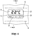
Figur 1- die Außenansicht einer Geräte-Frontblende mit Bedienungstasten und dem Flüssigkristalldisplay einer zugeordneten elektrischen Baugruppe,
Figur 2- die Baugruppe aus
Figur 1, geschnitten längs der Linie A-A dargestellt.
- Figure 1
- the external view of a device front panel with control buttons and the liquid crystal display of an assigned electrical module,
- Figure 2
- the assembly of Figure 1, shown along the line AA.
Figur 1 zeigt die Frontblende eines nicht dargestellten Elektrogerätes, benutzerseitig gesehen. Die Frontblende (1) ist mit einem Fenster (2) ausgestattet, in dem durch Tasten (3) abrufbare Informationen erkennbar sind. Mit rückseitig vorhandenen Stegen (4) ist die Frontblende (1) am Elektrogerät zu befestigen. Die Stege (4) werden auch zur Halterung der elektrischen Baugruppe (5) genutzt. Die Baugruppe ist mit einem Flüssigkristalldisplay (6) ausgestattet, deren Anzeigefläche (7) am Fenster (2) der Frontblende (1) anliegt.Figure 1 shows the front panel of an electrical device, not shown, seen by the user. The front panel (1) is equipped with a window (2) in which information that can be called up using buttons (3) can be recognized. The front panel (1) must be attached to the electrical device using webs (4) on the rear. The webs (4) are also used to hold the electrical assembly (5). The assembly is equipped with a liquid crystal display (6), the display surface (7) of which lies against the window (2) of the front panel (1).
Die elektrische Baugruppe (5) enthält als Untergruppe im wesentlichen eine bestückte Leiterplatte (8), einen Lichtleiter (10) und ein Flüssigkristalldisplay (6). Die Schaltung der Leiterplatte (8) ist über nicht dargestellte Anschlußeinrichtungen mit dem Elektrogerät elektrisch verbunden (Fig. 2). Die Leiterplatte (8) trägt auf ihrer der Frontblende (1) zugewandten Oberseite (9) einen Lichtleiter (10).The electrical assembly (5) essentially contains a printed circuit board (8), a light guide (10) and a liquid crystal display (6). The circuit of the circuit board (8) is electrically connected to the electrical device via connection devices (not shown) (FIG. 2). The circuit board (8) carries a light guide (10) on its upper side (9) facing the front panel (1).
Der Lichtleiter (10) hält in einer zur Leiterplatte (8) hin leicht konisch gestalteten, fensterartigen Ausnehmung (11) einen Leitgummistreifen (12). Der Leitgummistreifen (12) liegt mit seiner einen Kontaktfläche (13) gemeinsam mit dem Lichtleiter (10) auf der Leiterplatte (8) auf, mit seiner gegenüberliegenden Kontaktfläche (14) überragt er den Lichtleiter (10). Für eine lange Kontaktreihe wählt man mehrere fensterartige Ausnehmungen (11) und entsprechend unterteilte Leitgummistreifen (12). Leitgummistreifen (12) sind handelsüblich, sie bestehen aus elektrisch leitenden und elektrisch isolierenden Abschnitten, die sich in Längsrichtung des Leitgummistreifens in Abständen von wenigen Zehntel Millimetern abwechseld aneinanderreihen. Der Lichtleiter (10) ist anhand angeformter Zapfen (15), die in Bohrungen (16) eingreifen, an der Leiterplatte (8) ausgerichtet, und gegen Verschieben gesichert. Auf der Oberfläche (9) der Leiterplatte (8) sind nach Bedarf und nach verfügbarer Fläche bzw. verfügbarem Raum Bauelemente der Schaltung angeordnet, z.B. Widerstände (17); der Schaltkontakt (18) ist durch eine Freisparung (19) des Lichtleiters (10) hindurch von einer Taste (3) der Frontblende (1) zu betätigen; die Lampe (20) speist den Lichtleiter (10) mit Licht. Auf dem Lichtleiter (10) ist ein Flüssigkristalldisplay (6) auf Abstand zur Leiterplatte (8) angeordnet. Die Anschlußflächen des Flüssigkristalldisplays (6) liegen dabei auf der gegenüberliegenden Kontaktfläche (14) des Leitgummistreifens (12) auf und sind über dessen elektrisch leitenden Abschnitte mit der Leiterplatte (8) verbunden. Dem Lichtleiter sind Stege (22) angeformt, die hinsichtlich ihrer Verteilung der Kontur des Flüssigkristalldisplays (6) entsprechen und dessen Sollposition markieren. Das Flüssigkristalldisplay ist durch die Stege (22) gegen seitliches Verschieben geschützt.The light guide (10) holds a guide rubber strip (12) in a window-like recess (11) which is slightly conical towards the circuit board (8). The conductive rubber strip (12) rests with its one contact surface (13) together with the light guide (10) on the printed circuit board (8), with its opposite contact surface (14) it projects beyond the light guide (10). For a long row of contacts, one chooses several window-like recesses (11) and correspondingly divided conductive rubber strips (12). Conductive rubber strips (12) are commercially available, they consist of electrically conductive and electrically insulating sections which alternate in the longitudinal direction of the conductive rubber strip at intervals of a few tenths of a millimeter. The light guide (10) is aligned on the printed circuit board (8) by means of integrally formed pins (15) which engage in bores (16) and is secured against displacement. Components of the circuit, for example resistors (17), are arranged on the surface (9) of the printed circuit board (8) as required and according to the available area or space. the switch contact (18) can be actuated by a cutout (19) in the light guide (10) using a button (3) on the front panel (1); the lamp (20) feeds the light guide (10) with light. A liquid crystal display (6) is arranged at a distance from the circuit board (8) on the light guide (10). The connection surfaces of the liquid crystal display (6) lie on the opposite contact surface (14) of the conductive rubber strip (12) and are connected to the printed circuit board (8) via its electrically conductive sections. Webs (22) are formed on the light guide, which correspond in terms of their distribution to the contour of the liquid crystal display (6) and mark its desired position. The liquid crystal display is protected against lateral displacement by the webs (22).
Neben der Untergruppe enthält die Baugruppe (5) ein Abschirmblech (24), das die Untergruppe aufnimmt und das im wesentlichen parallel zur Unterseite (23) der Leiterplatte (8) der Untergruppe verläuft und das sich durch Sicken (25) gegen letztere abstützt. Ein Schenkel (26) des Abschirmbleches (24) ist einseitig um den Rand der Leiterplatte (8) herumgeführt. Der Schenkel (26) liegt mit einer Durchbiegung (30) seines Endabschnittes (27) in Linie parallel zu den Anschlußflächen des Flüssigkristalldisplays (6) etwa in Höhe des Leitgummistreifens (12) elastisch auf dem Flüssigkristalldisplay (6) auf und erzeugt eine zur Kontaktsicherung erforderliche Andrückkraft (P). Liegt die Berührungslinie des Endabschnittes (27) weiter entfernt vom Rand der Leiterplatte (8) als die dem Endabschnitt zugeordnete Sicke (25) auf der Unterseite der Leiterplatte, so entsteht eine Hebelwirkung, welche die Anordnung der Baugruppe in gegenseitiger Ausrichtung klammerartig zusammenhält. Das Abschirmblech (24) ist an der Seite, die dem Schenkel (26) gegenüberliegt mit einer Abwinkelung (29) versehen. Der Abstand der Abwinkelung (29) vom Schenkel (26) orientiert sich am entsprechenden Maß der aufzunehmenden Leiterplatte (8). Die Leiterplatte (8) liegt klemmend an der Abwinkelung (29) an. Der so geschaffene mechanische Verbund der Baugruppe (5) hält ausreichend bis zum endgültigen Einbau. Die Baugruppe (5) ist mittels ausgestellten Zungen (21) des Abschirmbleches (24) in Öffnungen (28) der Stege (4) an der Frontblende (1) gehalten.In addition to the sub-group, the assembly (5) contains a shielding plate (24) which receives the sub-group and which is essentially parallel to the The underside (23) of the circuit board (8) of the subassembly extends and is supported against the latter by beads (25). One leg (26) of the shielding plate (24) is guided on one side around the edge of the printed circuit board (8). The leg (26) lies with a deflection (30) of its end section (27) in line parallel to the connection surfaces of the liquid crystal display (6) approximately at the level of the conductive rubber strip (12) on the liquid crystal display (6) and generates a pressing force (P) required to ensure contact. If the line of contact of the end section (27) is further away from the edge of the printed circuit board (8) than the bead (25) assigned to the end section on the underside of the printed circuit board, a leverage effect arises which holds the arrangement of the assembly together like a clamp. The shielding plate (24) is provided with an angle (29) on the side opposite the leg (26). The distance of the bend (29) from the leg (26) is based on the corresponding dimension of the circuit board (8) to be accommodated. The circuit board (8) rests on the bend (29). The mechanical connection of the assembly (5) thus created lasts sufficiently until it is finally installed. The assembly (5) is held in the openings (28) of the webs (4) on the front panel (1) by means of tongues (21) in the shielding plate (24).
Der Zusammenbau der Baugruppe (5) erfolgt, indem zunächst der Lichtleiter (10) mit dem darin eingesetzten Leitgummistreifen (12) auf die bebestückte Leiterplatte (8) aufgesetzt und an den Bohrungen (16) ausgerichtet wird, dann das Flüssigkristalldisplay (6) auf dem Lichtleiter (10) plaziert und nachfolgend das gesamte, eine Untgergruppe darstellende Paket unter Schwenken unter den Endabschnitt (27) des Schenkels (26) geschoben wird. Dabei wird der Endabschnitt (27) gespannt.
Claims (8)
dadurch gekennzeichnet,
daß die Untergruppe (6,8,10,12) nur einseitig zusammengehalten ist und auf der gegenüberliegenden Seite an einer Abwinkelung (29) des Abschirmbleches (24) klemmend anliegt und daß der Endabschnitt (27) eine parallel zum Rand verlaufende Durchbiegung (30) aufweist, die im Abstand zum Rand federnd auf der Untergruppe (6,8,10,12) aufliegt.Electrical assembly (5) with a sandwich-like sub-assembly (6,8,10,12), which has at least one printed circuit board (8), a liquid crystal display (6) and a device (10,12) for storing and contacting the liquid crystal display (6) comprises, and with a shielding plate (24) on the back (23) of the sub-group (6,8,10,12), which receives the sub-group and which surrounds the edge of the sub-group with an end section (27) the sub-group (6,8 , 10,12) holds together,
characterized,
that the sub-group (6, 8, 10, 12) is held together only on one side and bears on the opposite side against a bend (29) of the shielding plate (24) and that the end section (27) has a bend (30) running parallel to the edge which rests resiliently on the sub-group (6,8,10,12) at a distance from the edge.
dadurch gekennzeichnet,
daß das Abschirmblech (24) an der Rückseite (23) der Untergruppe eine oder mehrere, die Untergruppe (6,8,10,12) abstützende Sicke (25) aufweist und eine Sicke (25) der Durchbiegung (30) zugeordnet ist.Electrical assembly according to claim 1,
characterized,
that the shielding plate (24) on the rear (23) of the subgroup has one or more beads (25) supporting the subgroup (6, 8, 10, 12) and a bead (25) is assigned to the deflection (30).
dadurch gekennzeichnet,
daß die Einrichtung (10,12) ein Lichtleiter (10) ist mit einem Durchbruch (11) zur Halterung von Kontaktelementen (12) für die Kontaktierung von Flüssigkristalldisplay (6) und Leiterplatte (8).Electrical assembly according to claim 1 or claim 2,
characterized,
that the device (10, 12) is a light guide (10) with an opening (11) for holding contact elements (12) for contacting the liquid crystal display (6) and printed circuit board (8).
dadurch gekennzeichnet,
daß zur Kontaktierung ein Leitgummistreifen (12) benutzt ist.Electrical assembly according to claim 3,
characterized,
that a conductive rubber strip (12) is used for contacting.
dadurch gekennzeichnet,
daß die Durchbiegung (30) in Höhe der Kontaktierung (13,14) auf die Untergruppe drückt.Electrical assembly according to one of claims 1 to 4,
characterized,
that the deflection (30) at the level of the contact (13, 14) presses on the sub-group.
dadurch gekennzeichnet,
daß die Leiterplatte (8) der Untergruppe (6,8,10,12) an der Abwinkelung (29) anliegt.Electrical assembly according to one of claims 1 to 5,
characterized,
that the circuit board (8) of the sub-group (6,8,10,12) bears against the bend (29).
dadurch gekennzeichnet,
daß die Leiterplatte (8) Bohrungen (16) aufweist, auf deren Rand sich der Lichtleiter (10) abstützt und in die er mittels angeformter Zapfen (15) verschiebefest eingreift.Electrical assembly according to one of claims 1 to 6,
characterized,
that the circuit board (8) has bores (16), on the edge of which the light guide (10) is supported and in which it engages in a displaceable manner by means of integrally formed pins (15).
dadurch gekennzeichnet,
daß eine Fläche des Lichtleiters (10) das Flüssigkristalldisplay (6) an Markierungen (22) ausgerichtet auf Abstand zur Leiterplatte (8) trägt.Electrical assembly according to one of claims 1 to 7,
characterized,
that a surface of the light guide (10) carries the liquid crystal display (6) at markings (22) aligned at a distance from the circuit board (8).
Applications Claiming Priority (2)
| Application Number | Priority Date | Filing Date | Title |
|---|---|---|---|
| DE4236353 | 1992-10-28 | ||
| DE4236353A DE4236353C2 (en) | 1992-10-28 | 1992-10-28 | Electrical assembly |
Publications (2)
| Publication Number | Publication Date |
|---|---|
| EP0594987A1 true EP0594987A1 (en) | 1994-05-04 |
| EP0594987B1 EP0594987B1 (en) | 1996-10-23 |
Family
ID=6471535
Family Applications (1)
| Application Number | Title | Priority Date | Filing Date |
|---|---|---|---|
| EP93114234A Expired - Lifetime EP0594987B1 (en) | 1992-10-28 | 1993-09-06 | Electric module |
Country Status (4)
| Country | Link |
|---|---|
| US (1) | US5333099A (en) |
| EP (1) | EP0594987B1 (en) |
| JP (1) | JP3347842B2 (en) |
| DE (2) | DE4236353C2 (en) |
Cited By (3)
| Publication number | Priority date | Publication date | Assignee | Title |
|---|---|---|---|---|
| FR2768838A1 (en) * | 1997-09-25 | 1999-03-26 | Magneti Marelli France | Anti-vibration mounting for automobile liquid crystal cell dashboard display. |
| EP1906717A2 (en) * | 2006-09-28 | 2008-04-02 | Diehl AKO Stiftung & Co. KG | Component assembly |
| FR3011972A1 (en) * | 2013-10-15 | 2015-04-17 | Johnson Contr Automotive Elect | DEVICE FOR POSITIONING AND FIXING A DISPLAY ELEMENT AND DISPLAY DEVICE |
Families Citing this family (8)
| Publication number | Priority date | Publication date | Assignee | Title |
|---|---|---|---|---|
| DE4238928C1 (en) * | 1992-11-19 | 1994-04-07 | Preh Elektro Feinmechanik | Lamp holder for an electrical assembly |
| DE19516348C2 (en) * | 1995-05-04 | 1998-04-09 | Valeo Borg Instr Verw Gmbh | Contact device |
| DE19621919A1 (en) * | 1996-05-31 | 1997-12-04 | Hella Kg Hueck & Co | Display device for motor vehicles |
| DE19734859C2 (en) * | 1997-08-12 | 2001-02-22 | Bosch Gmbh Robert | Display and operating device of an electrical device |
| JP4298068B2 (en) * | 1998-08-18 | 2009-07-15 | セイコーエプソン株式会社 | ELECTRO-OPTICAL DEVICE, ELECTRONIC DEVICE EQUIPPED WITH THE SAME, AND METHOD FOR PRODUCING ELECTRO-OPTICAL DEVICE |
| KR100813470B1 (en) * | 2001-11-27 | 2008-03-13 | 삼성전자주식회사 | Conductive member and liquid crystal display device having the same |
| KR100940334B1 (en) * | 2007-12-10 | 2010-02-04 | 주식회사 토비스 | Liquid Crystal Display Module and Portable Phone Having the Same |
| CN102425770A (en) * | 2011-11-25 | 2012-04-25 | 深圳市华星光电技术有限公司 | Light bar fixing device, backlight module and liquid crystal display |
Citations (3)
| Publication number | Priority date | Publication date | Assignee | Title |
|---|---|---|---|---|
| BE881912A (en) * | 1980-02-26 | 1980-06-16 | Haens Joseph P M D | WERKWIJZE VOOR HET VERWEZENLIJKEN VAN UITLEESEENHEDEN UIT VLOEIBARE KRISTALLEN MET GEINTEGREERDE AANSTUUREENHEID EN UITLEESEENHEDEN |
| DE8805722U1 (en) * | 1988-04-30 | 1988-06-09 | Blaupunkt-Werke Gmbh, 3200 Hildesheim, De | |
| US4789224A (en) * | 1987-05-04 | 1988-12-06 | General Motors Corporation | Instrument panel having light pipe having legs |
Family Cites Families (8)
| Publication number | Priority date | Publication date | Assignee | Title |
|---|---|---|---|---|
| JPS58209777A (en) * | 1982-05-31 | 1983-12-06 | 日本精機株式会社 | Liquid crystal display |
| JPS62140792U (en) * | 1986-02-28 | 1987-09-05 | ||
| DE8705715U1 (en) * | 1987-04-18 | 1987-10-15 | Walter Esser Gmbh + Co Kg Kunststoff-Spritzgiesserei Und Werkzeugbau, 2947 Friedeburg, De | |
| DE3726225C1 (en) * | 1987-08-07 | 1988-08-04 | Telefonbau & Normalzeit Gmbh | Display device with a liquid crystal display |
| DE8801014U1 (en) * | 1988-01-28 | 1989-05-24 | Bethe, Uwe, 3550 Marburg, De | |
| US5117330A (en) * | 1990-04-09 | 1992-05-26 | Hewlett-Packard Company | Fixture for circuit components |
| JP3060654B2 (en) * | 1990-12-27 | 2000-07-10 | セイコーエプソン株式会社 | Liquid crystal display |
| DE4105505A1 (en) * | 1991-02-22 | 1992-09-03 | Telefonbau & Normalzeit Gmbh | Liquid crystal display device with large number of electrode connections - uses distance piece to separate compressable conducting blocks, enabling two rows of connections to be employed |
-
1992
- 1992-10-28 DE DE4236353A patent/DE4236353C2/en not_active Expired - Fee Related
-
1993
- 1993-09-06 DE DE59304286T patent/DE59304286D1/en not_active Expired - Lifetime
- 1993-09-06 EP EP93114234A patent/EP0594987B1/en not_active Expired - Lifetime
- 1993-10-19 JP JP26119293A patent/JP3347842B2/en not_active Expired - Fee Related
- 1993-10-25 US US08/141,026 patent/US5333099A/en not_active Expired - Fee Related
Patent Citations (3)
| Publication number | Priority date | Publication date | Assignee | Title |
|---|---|---|---|---|
| BE881912A (en) * | 1980-02-26 | 1980-06-16 | Haens Joseph P M D | WERKWIJZE VOOR HET VERWEZENLIJKEN VAN UITLEESEENHEDEN UIT VLOEIBARE KRISTALLEN MET GEINTEGREERDE AANSTUUREENHEID EN UITLEESEENHEDEN |
| US4789224A (en) * | 1987-05-04 | 1988-12-06 | General Motors Corporation | Instrument panel having light pipe having legs |
| DE8805722U1 (en) * | 1988-04-30 | 1988-06-09 | Blaupunkt-Werke Gmbh, 3200 Hildesheim, De |
Cited By (4)
| Publication number | Priority date | Publication date | Assignee | Title |
|---|---|---|---|---|
| FR2768838A1 (en) * | 1997-09-25 | 1999-03-26 | Magneti Marelli France | Anti-vibration mounting for automobile liquid crystal cell dashboard display. |
| EP1906717A2 (en) * | 2006-09-28 | 2008-04-02 | Diehl AKO Stiftung & Co. KG | Component assembly |
| EP1906717A3 (en) * | 2006-09-28 | 2010-01-20 | Diehl AKO Stiftung & Co. KG | Component assembly |
| FR3011972A1 (en) * | 2013-10-15 | 2015-04-17 | Johnson Contr Automotive Elect | DEVICE FOR POSITIONING AND FIXING A DISPLAY ELEMENT AND DISPLAY DEVICE |
Also Published As
| Publication number | Publication date |
|---|---|
| JP3347842B2 (en) | 2002-11-20 |
| JPH06214222A (en) | 1994-08-05 |
| DE4236353A1 (en) | 1994-05-05 |
| DE59304286D1 (en) | 1996-11-28 |
| US5333099A (en) | 1994-07-26 |
| DE4236353C2 (en) | 1995-03-23 |
| EP0594987B1 (en) | 1996-10-23 |
Similar Documents
| Publication | Publication Date | Title |
|---|---|---|
| EP0013335A1 (en) | Arrangement for electrically connecting a multiplicity of contacts | |
| EP0594987B1 (en) | Electric module | |
| EP0221278B1 (en) | Support for printed circuits arranged in a rack | |
| DE69823500T2 (en) | ELECTROLUMINESCENT LIGHT | |
| EP0123905A2 (en) | Over-voltage protection device for addition to a distributor | |
| DE3326972C2 (en) | ||
| DE2245415B2 (en) | Compact electronic calculator | |
| EP0022934A1 (en) | Electrooptical display device, especially liquid crystal display | |
| EP0104304B1 (en) | Car radio | |
| DE2812332B2 (en) | Multiple connector for cards with printed circuit boards | |
| EP1905122A1 (en) | Electronic device for a vehicle having a printed circuit board with which there is direct contact | |
| DE3906592A1 (en) | Motor-vehicle antenna, preferably for VHF broadcast-radio reception | |
| EP0679051A2 (en) | Contacting actuating and display means | |
| DE3144535C2 (en) | Display device with liquid crystal display | |
| DE8321095U1 (en) | Optical display device for telephone subscriber stations | |
| DE3308510A1 (en) | Housing for electrical and/or electronic components | |
| EP0175942A1 (en) | Frame for receiving slidable electrical equipments | |
| DE1848651U (en) | CONTACT DEVICE FOR PRINTED CIRCUITS. | |
| EP0910234A2 (en) | Function module with indicator for automation apparatus | |
| DE3313080A1 (en) | Device for contacting a display unit to a liquid crystal layer | |
| WO1997049147A1 (en) | Socket connector for plug-in connections between a printed board and a wiring backplane | |
| DD273141A1 (en) | ARRANGEMENT FOR DUST AND SPLASH-SAFE INSTALLATION OF CONTROL ELEMENTS IN AN OPERATOR PANEL | |
| DE2041805A1 (en) | Cover plate for housing with slide-in circuit boards | |
| DE4210200C2 (en) | Electronics module | |
| DE3132966A1 (en) | Operating panel for desk-top telephones |
Legal Events
| Date | Code | Title | Description |
|---|---|---|---|
| PUAI | Public reference made under article 153(3) epc to a published international application that has entered the european phase |
Free format text: ORIGINAL CODE: 0009012 |
|
| AK | Designated contracting states |
Kind code of ref document: A1 Designated state(s): DE FR GB IT |
|
| 17P | Request for examination filed |
Effective date: 19940321 |
|
| GRAG | Despatch of communication of intention to grant |
Free format text: ORIGINAL CODE: EPIDOS AGRA |
|
| GRAH | Despatch of communication of intention to grant a patent |
Free format text: ORIGINAL CODE: EPIDOS IGRA |
|
| GRAH | Despatch of communication of intention to grant a patent |
Free format text: ORIGINAL CODE: EPIDOS IGRA |
|
| 17Q | First examination report despatched |
Effective date: 19960322 |
|
| GRAA | (expected) grant |
Free format text: ORIGINAL CODE: 0009210 |
|
| AK | Designated contracting states |
Kind code of ref document: B1 Designated state(s): DE FR GB IT |
|
| ITF | It: translation for a ep patent filed |
Owner name: DR. ING. A. RACHELI & C. |
|
| ET | Fr: translation filed | ||
| GBT | Gb: translation of ep patent filed (gb section 77(6)(a)/1977) |
Effective date: 19961023 |
|
| REF | Corresponds to: |
Ref document number: 59304286 Country of ref document: DE Date of ref document: 19961128 |
|
| PLBE | No opposition filed within time limit |
Free format text: ORIGINAL CODE: 0009261 |
|
| STAA | Information on the status of an ep patent application or granted ep patent |
Free format text: STATUS: NO OPPOSITION FILED WITHIN TIME LIMIT |
|
| 26N | No opposition filed | ||
| REG | Reference to a national code |
Ref country code: GB Ref legal event code: IF02 |
|
| PGFP | Annual fee paid to national office [announced via postgrant information from national office to epo] |
Ref country code: GB Payment date: 20020904 Year of fee payment: 10 |
|
| PGFP | Annual fee paid to national office [announced via postgrant information from national office to epo] |
Ref country code: FR Payment date: 20020909 Year of fee payment: 10 |
|
| PG25 | Lapsed in a contracting state [announced via postgrant information from national office to epo] |
Ref country code: GB Free format text: LAPSE BECAUSE OF NON-PAYMENT OF DUE FEES Effective date: 20030906 |
|
| GBPC | Gb: european patent ceased through non-payment of renewal fee |
Effective date: 20030906 |
|
| PG25 | Lapsed in a contracting state [announced via postgrant information from national office to epo] |
Ref country code: FR Free format text: LAPSE BECAUSE OF NON-PAYMENT OF DUE FEES Effective date: 20040528 |
|
| REG | Reference to a national code |
Ref country code: FR Ref legal event code: ST |
|
| PG25 | Lapsed in a contracting state [announced via postgrant information from national office to epo] |
Ref country code: IT Free format text: LAPSE BECAUSE OF NON-PAYMENT OF DUE FEES;WARNING: LAPSES OF ITALIAN PATENTS WITH EFFECTIVE DATE BEFORE 2007 MAY HAVE OCCURRED AT ANY TIME BEFORE 2007. THE CORRECT EFFECTIVE DATE MAY BE DIFFERENT FROM THE ONE RECORDED. Effective date: 20050906 |
|
| PGFP | Annual fee paid to national office [announced via postgrant information from national office to epo] |
Ref country code: DE Payment date: 20090922 Year of fee payment: 17 |
|
| REG | Reference to a national code |
Ref country code: DE Ref legal event code: R119 Ref document number: 59304286 Country of ref document: DE Effective date: 20110401 |
|
| PG25 | Lapsed in a contracting state [announced via postgrant information from national office to epo] |
Ref country code: DE Free format text: LAPSE BECAUSE OF NON-PAYMENT OF DUE FEES Effective date: 20110401 |