EP0591032A1 - Gegentaktleistungsverstärker mit Gegenkopplungstransformatoren für metrische Wellen - Google Patents
Gegentaktleistungsverstärker mit Gegenkopplungstransformatoren für metrische Wellen Download PDFInfo
- Publication number
- EP0591032A1 EP0591032A1 EP93402337A EP93402337A EP0591032A1 EP 0591032 A1 EP0591032 A1 EP 0591032A1 EP 93402337 A EP93402337 A EP 93402337A EP 93402337 A EP93402337 A EP 93402337A EP 0591032 A1 EP0591032 A1 EP 0591032A1
- Authority
- EP
- European Patent Office
- Prior art keywords
- amplifier
- output
- input
- transformer
- transistors
- Prior art date
- Legal status (The legal status is an assumption and is not a legal conclusion. Google has not performed a legal analysis and makes no representation as to the accuracy of the status listed.)
- Granted
Links
Images
Classifications
-
- H—ELECTRICITY
- H03—ELECTRONIC CIRCUITRY
- H03F—AMPLIFIERS
- H03F1/00—Details of amplifiers with only discharge tubes, only semiconductor devices or only unspecified devices as amplifying elements
- H03F1/34—Negative-feedback-circuit arrangements with or without positive feedback
- H03F1/347—Negative-feedback-circuit arrangements with or without positive feedback using transformers
-
- H—ELECTRICITY
- H03—ELECTRONIC CIRCUITRY
- H03F—AMPLIFIERS
- H03F3/00—Amplifiers with only discharge tubes or only semiconductor devices as amplifying elements
- H03F3/26—Push-pull amplifiers; Phase-splitters therefor
- H03F3/265—Push-pull amplifiers; Phase-splitters therefor with field-effect transistors only
Definitions
- the present invention relates to a push-pull power amplifier counter-reacted by VHF transformers. It applies in particular to the production of portable radio transmitters operating close to other transmitters.
- the resistance feedback leads to a loss of power due to the additional power dissipation in the feedback resistors as well as an increase in the power dissipation in the transistors, which is felt on the efficiency of the amplifier which is an important feature for a power amplifier.
- the behavior of the amplifier with regard to mismatched loads is not satisfactory: the supply current of the amplifier varies as a function of the load present at the output of the amplifier.
- this behavior can be improved by decreasing the value of the feedback resistors, but to the detriment of the gain and the efficiency of the amplifier.
- the object of the invention is to overcome the aforementioned drawbacks.
- the subject of the invention is a power amplifier of the push-pull type with two counter-reactive transistors comprising an adaptation transformer respectively at the input and at the output of the amplifier, characterized in that it comprises a double winding feedback transformer respectively connected at the input and output of each of the transistors, such that the drain of each transistor is coupled to its respective gate by the input feedback transformer to which it is connected and such that the gate of each transistor is coupled to its drain by the output feedback transformer to which it is connected, in that the sources of the two transistors are connected to the ground potential of the amplifier supply, and in that the gates are respectively connected at one end of the secondary winding of the input matching transformer and in that the drains are respectively connected to one end of the primary winding of the output transformer.
- the main advantage of the invention is that it makes it possible to improve the gain, the efficiency and the behavior of the amplifier with respect to input-output adaptation problems. For this, we replace the simple feedback using resistors between the output and the input of the amplifier by a double feedback using only double winding transformers.
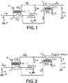
- FIG. 1 illustrates an embodiment of an amplifier with a single MOS transistor counter-reacted by two transformers making it possible to describe the basic structure of a push-pull amplifier according to the invention which will be described later.
- the amplifier which is shown in FIG. 1, organized around a ground circuit M serving as a potential reference, comprises an MOS transistor 1 coupled to two feedback circuits formed by two transformers T1 and T2 shown in inside a broken line.
- the secondary winding 4 of this same transformer is connected by one of its ends at the ground potential of the amplifier and by its other end to the drain 5 of the transistor 1.
- the transformation ratios of the two transformers T1 and T2 respectively in voltage and in current are chosen equal to 6.
- the transformer T1 provides a series voltage feedback, that is to say that the quantity taken at the output of the amplifier is a voltage, and a quantity which is proportional to it is fed back into series at the input of the amplifier. .
- the transformer T2 ensures a parallel current feedback, that is to say that the quantity taken at the output of the amplifier is a current, and a quantity which is proportional to it is reinjected in parallel on the input of the 'amplifier.
- a current i is injected at the input of the amplifier on the primary winding 2 of the input transformer T1 and a voltage u is applied between the input E and the ground potential M.
- the potential u is also found at the terminals of the primary winding 2 of the input feedback transformer T1, the MOS transistor being considered as perfect and the transformer T2 as the ideal current transformer with u' ⁇ 0.
- On the secondary winding 4 of the input transformer T1 taking into account the voltage transformation ratio of the previous example equal to n4 / n2 6, there is a voltage -6u. This voltage is also found between the output S of the amplifier and the ground potential M.
- the primary winding 6 of the output transformer T2, disposed between the gate 3 and the ground potential M, is traversed by the same input current i, the transistor 1 being considered as perfect, its gate current is zero.
- FIG. 2 represents the amplifier circuit of FIG. 1 closed on a short circuit 8.
- FIG. 2 represents the amplifier circuit of FIG. 1 closed on a short circuit 8.
- the elements identical to FIG. 1 are designated by the same references.
- the input excitation current is equal to 2i
- the current flowing in the secondary 4 of the input transformer T1 is equal to (-2/6) i
- the drain current of transistor 1 equal to 11.6 i.
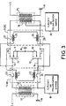
- This adaptation consists in fact in the production of a push-pull amplifier known per se but counter-reacted at input and output by transformers with double winding according to the invention
- each transistor 11 and 12 are respectively coupled to one end of the secondary winding 15 of an adaptation transformer Te, represented inside a broken line, at the input of the amplifier, and the drains 16 and 17 of each transistor 11 and 12 are respectively coupled to one end of the primary winding 18 of a matching transformer TS, also shown inside a broken line, at the output of the amplifier.
- Te adaptation transformer
- TS matching transformer
- Two bias circuits 19 and 20 supply the gates 13 and 14 and the drains 16 and 17 respectively of the MOS transistors 11 and 12.
- the input and output feedback from the push-pull amplifier is provided by two input and output feedback transformers of the MOS transistors 11 and 12.
- Each transformer has a double primary and secondary winding and can for example be designed with a ferrite of the type known under the name of BALUN.
- the input feedback transformer TCRE comprises two secondary windings in series 21 and 22, the two ends of which are connected respectively to the drain 16 and 17 of each MOS transistor 11 and 12.
- Each primary winding 23 and 24 is disposed respectively between the gates 13 and 14 of the transistors 11 and 12 and each of the ends of the secondary winding 15 of the adaptation transformer at the TE input of the amplifier.
- the output feedback transformer TCRS comprises two primary windings in series 25 and 26, the two ends of which are connected respectively to the gate of each MOS transistor 11 and 12.
- Each secondary winding 27 and 28 is disposed respectively between the drain 16 and 17 of the transistors 11 and 12 and each of the ends of the primary winding 18 of the adaptation transformer at the output TS of the amplifier.
- the double feedback thus produced by transformers makes it possible to obtain a higher efficiency than that obtained by feedback resistors, for example, for an identical input power of 22 dBm at 60 MHz, the inputs and outputs being loaded. by the same impedances, the efficiency of the amplifier feedback from transformers is 63.2%, that of the amplifier feedback from resistors being 48.5%.
- the feedback resistors dissipate a certain power involved in the calculation of the overall efficiency of the amplifier while the transformers practically do not dissipate power because of their very low winding resistance. There is therefore less energy loss with a feedback by transformers rather than with a feedback by resistors.
- the input and output impedances of the amplifier are higher than with a resistance feedback, the impedances approaching the characteristic impedance of 50 ⁇ .
- this type of circuit transmits the output impedance of the amplifier to its input.
- the advantage of such a circuit is explained below.
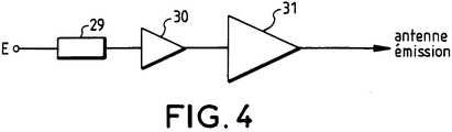
- a power amplifier is generally placed at the output of an amplifier chain in front of the transmitting antenna. This amplifying chain is illustrated in FIG. 4.
- This amplifier chain includes input to the antenna, an attenuator 29, a preamplifier 30 and a power amplifier 31.
- the power amplifier 31 is the push-pull amplifier according to the invention, the output impedance of the amplifier is therefore transmitted on its input and also corresponds to the output of the preamplifier 30 which is at the head of the amplifying chain.
- the strong mismatch at the output of the push-pull amplifier 31 is transmitted directly to the output of the preamplifier 30, its output power collapses and therefore the excitation power of the push-pull amplifier 31 decreases, thus avoiding significant consumption of the transistors of the amplifier 31.
- a push-pull amplifier according to the invention in accordance with that of FIG. 3, made it possible to obtain the following results which are compared for information with a push-pull amplifier, with simple feedback output-input by resistors, placed under the same conditions as the push-pull with transformers:
- the amplifier according to the invention provides an output power close to 1.9 W at 6.5 v in the VHF frequency range (30-88 MHZ) and accepts an output mismatch having a TOS of up to 10.
- the TOS obtained under these conditions at the output of the amplifier according to the invention is:
- the supply current of the amplifier according to the invention varies less on mismatches bringing low charges. This variation does not exceed 0.8 A for the amplifier according to the invention against a variation of 1.2 A for an amplifier counter-reacted by resistors.
- the double feedback by transformers allows a better adaptation in input and output of the amplifier according to the invention with input and output impedance values closer to 50 ⁇ which is the value of the characteristic impedance.
- the efficiency of the double feedback by transformers depends on the choice of the transformation ratios of the feedback transformers at the input and at the output of the amplifier.
Landscapes
- Engineering & Computer Science (AREA)
- Power Engineering (AREA)
- Amplifiers (AREA)
Applications Claiming Priority (2)
| Application Number | Priority Date | Filing Date | Title |
|---|---|---|---|
| FR9211580A FR2696296B1 (fr) | 1992-09-29 | 1992-09-29 | Amplificateur de puissance push-pull contre-réactionné par transformateurs en ondes métriques. |
| FR9211580 | 1992-09-29 |
Publications (2)
| Publication Number | Publication Date |
|---|---|
| EP0591032A1 true EP0591032A1 (de) | 1994-04-06 |
| EP0591032B1 EP0591032B1 (de) | 1997-12-03 |
Family
ID=9433995
Family Applications (1)
| Application Number | Title | Priority Date | Filing Date |
|---|---|---|---|
| EP19930402337 Expired - Lifetime EP0591032B1 (de) | 1992-09-29 | 1993-09-24 | Gegentaktleistungsverstärker mit Gegenkopplungstransformatoren für metrische Wellen |
Country Status (3)
| Country | Link |
|---|---|
| EP (1) | EP0591032B1 (de) |
| DE (1) | DE69315528T2 (de) |
| FR (1) | FR2696296B1 (de) |
Cited By (3)
| Publication number | Priority date | Publication date | Assignee | Title |
|---|---|---|---|---|
| US7123090B2 (en) * | 2003-06-06 | 2006-10-17 | Bruker Biospin Mri Gmbh | Low-noise preamplifier, in particular, for nuclear magnetic resonance (NMR) |
| US7432764B2 (en) | 2005-08-12 | 2008-10-07 | Seimens Aktiengesellschaft | Push-pull amplifier with transformational negative feedback |
| WO2010007177A1 (en) * | 2008-07-17 | 2010-01-21 | Stichting Imec Nederland | Dual-loop feedback amplifying circuit |
Citations (2)
| Publication number | Priority date | Publication date | Assignee | Title |
|---|---|---|---|---|
| US4314252A (en) * | 1980-11-14 | 1982-02-02 | Rockwell International Corporation | Preamplifier for ADF loop antenna |
| US4590434A (en) * | 1983-05-06 | 1986-05-20 | New England Microwave Corporation | High dynamic range amplifier with low noise and low distortion |
-
1992
- 1992-09-29 FR FR9211580A patent/FR2696296B1/fr not_active Expired - Lifetime
-
1993
- 1993-09-24 EP EP19930402337 patent/EP0591032B1/de not_active Expired - Lifetime
- 1993-09-24 DE DE1993615528 patent/DE69315528T2/de not_active Expired - Lifetime
Patent Citations (2)
| Publication number | Priority date | Publication date | Assignee | Title |
|---|---|---|---|---|
| US4314252A (en) * | 1980-11-14 | 1982-02-02 | Rockwell International Corporation | Preamplifier for ADF loop antenna |
| US4590434A (en) * | 1983-05-06 | 1986-05-20 | New England Microwave Corporation | High dynamic range amplifier with low noise and low distortion |
Non-Patent Citations (1)
| Title |
|---|
| U.L. ROHDE,DJ2LR, 52 HILLCREST DRIVE, UPPER SADDLE RIVER, NJ 07458: "OPTIMUM DESIGN FOR HIGH-FREQUENCY COMMUNICATIONS RECEIVERS", HAM RADIO, October 1976 (1976-10-01), US, pages 10 - 25, XP002069046 * |
Cited By (4)
| Publication number | Priority date | Publication date | Assignee | Title |
|---|---|---|---|---|
| US7123090B2 (en) * | 2003-06-06 | 2006-10-17 | Bruker Biospin Mri Gmbh | Low-noise preamplifier, in particular, for nuclear magnetic resonance (NMR) |
| US7432764B2 (en) | 2005-08-12 | 2008-10-07 | Seimens Aktiengesellschaft | Push-pull amplifier with transformational negative feedback |
| WO2010007177A1 (en) * | 2008-07-17 | 2010-01-21 | Stichting Imec Nederland | Dual-loop feedback amplifying circuit |
| US8446217B2 (en) | 2008-07-17 | 2013-05-21 | Imec | Dual-loop feedback amplifying circuit |
Also Published As
| Publication number | Publication date |
|---|---|
| DE69315528D1 (de) | 1998-01-15 |
| EP0591032B1 (de) | 1997-12-03 |
| DE69315528T2 (de) | 1998-04-02 |
| FR2696296A1 (fr) | 1994-04-01 |
| FR2696296B1 (fr) | 1994-10-28 |
Similar Documents
| Publication | Publication Date | Title |
|---|---|---|
| EP0563373A1 (de) | Richtkoppler/verzweigerschaltung für Mittelfrequenz Trägerstrom auf Niederspannungsleitung. | |
| FR2485314A1 (fr) | Circuit de transmission en sortie de microphone | |
| EP1388935B1 (de) | Aktive Lastvorrichtung zum Einstellen einer Ultrabreitbandkettenverstärkerschaltung mit Verstärkungsregelung | |
| EP0592281B1 (de) | Breitbandiger Hochfrequenzleistungsverstärker | |
| FR2608862A1 (fr) | Commutateur electronique a tres haute frequence | |
| EP0591032B1 (de) | Gegentaktleistungsverstärker mit Gegenkopplungstransformatoren für metrische Wellen | |
| EP0737003B1 (de) | Ausleseverstärker für CCD-Register | |
| EP0455570A1 (de) | Sehr breitbandige Verstärkungseinrichtung für Gleichstrom bis Mikrowellen, insbesondere geeignet für integrierte Schaltungen | |
| FR2721155A1 (fr) | Commutateur haute fréquence unipolaire à plusieurs directions fonctionnant avec gain. | |
| EP0237099A1 (de) | Breitbandkettenverstärkerschaltung im Ultrahochfrequenzbereich | |
| EP0529734B1 (de) | Verstärkereinrichtung für ein Kabelfernseh-Verteilungsnetz | |
| US11552608B2 (en) | Wideband distributed power amplifiers and systems and methods thereof | |
| FR3120758A1 (fr) | Circuit de polarisation en bande de base et rf, et circuit amplificateur de puissance rf le comprenant | |
| EP0060164A1 (de) | Linearer, in gleitendem Klasse A-Betrieb arbeitender Breitbandverstärker mit niedrigem Verbrauch und Schaltung mit wenigstens einem solchen Verstärker | |
| FR2696063A1 (fr) | Système de coupleur pour transmission duplex. | |
| EP3275084B1 (de) | Strom-/daten-elektroverbinder | |
| EP1554799B1 (de) | Integrierte hf-verstärkerschaltung | |
| EP0285483A1 (de) | Breitbandverstärker mit geringem Rauschen für metrische Wellen | |
| FR2573262A1 (fr) | Amplificateur a large bande et faible bruit en ondes metriques | |
| FR3157968A1 (fr) | Limiteur radiofréquence | |
| FR2882204A1 (fr) | Circuit amplificateur large bande et circuit de polarisation | |
| WO2020049057A1 (fr) | Etage de sortie classe a notamment pour casque audio | |
| BE431146A (de) | ||
| CH718177A2 (fr) | Système de commande pour étiquettes passives RFID UHF. | |
| FR2482385A1 (fr) | Circuit de reglage de gain |
Legal Events
| Date | Code | Title | Description |
|---|---|---|---|
| PUAI | Public reference made under article 153(3) epc to a published international application that has entered the european phase |
Free format text: ORIGINAL CODE: 0009012 |
|
| AK | Designated contracting states |
Kind code of ref document: A1 Designated state(s): DE GB IT |
|
| 17P | Request for examination filed |
Effective date: 19940922 |
|
| GRAG | Despatch of communication of intention to grant |
Free format text: ORIGINAL CODE: EPIDOS AGRA |
|
| 17Q | First examination report despatched |
Effective date: 19961220 |
|
| GRAH | Despatch of communication of intention to grant a patent |
Free format text: ORIGINAL CODE: EPIDOS IGRA |
|
| GRAH | Despatch of communication of intention to grant a patent |
Free format text: ORIGINAL CODE: EPIDOS IGRA |
|
| GRAA | (expected) grant |
Free format text: ORIGINAL CODE: 0009210 |
|
| AK | Designated contracting states |
Kind code of ref document: B1 Designated state(s): DE GB IT |
|
| ITF | It: translation for a ep patent filed | ||
| REF | Corresponds to: |
Ref document number: 69315528 Country of ref document: DE Date of ref document: 19980115 |
|
| GBT | Gb: translation of ep patent filed (gb section 77(6)(a)/1977) |
Effective date: 19980205 |
|
| PLBE | No opposition filed within time limit |
Free format text: ORIGINAL CODE: 0009261 |
|
| STAA | Information on the status of an ep patent application or granted ep patent |
Free format text: STATUS: NO OPPOSITION FILED WITHIN TIME LIMIT |
|
| 26N | No opposition filed | ||
| REG | Reference to a national code |
Ref country code: GB Ref legal event code: IF02 |
|
| PG25 | Lapsed in a contracting state [announced via postgrant information from national office to epo] |
Ref country code: IT Free format text: LAPSE BECAUSE OF NON-PAYMENT OF DUE FEES;WARNING: LAPSES OF ITALIAN PATENTS WITH EFFECTIVE DATE BEFORE 2007 MAY HAVE OCCURRED AT ANY TIME BEFORE 2007. THE CORRECT EFFECTIVE DATE MAY BE DIFFERENT FROM THE ONE RECORDED. Effective date: 20050924 |
|
| PGFP | Annual fee paid to national office [announced via postgrant information from national office to epo] |
Ref country code: GB Payment date: 20120919 Year of fee payment: 20 |
|
| PGFP | Annual fee paid to national office [announced via postgrant information from national office to epo] |
Ref country code: DE Payment date: 20120919 Year of fee payment: 20 |
|
| REG | Reference to a national code |
Ref country code: DE Ref legal event code: R071 Ref document number: 69315528 Country of ref document: DE |
|
| REG | Reference to a national code |
Ref country code: GB Ref legal event code: PE20 Expiry date: 20130923 |
|
| PG25 | Lapsed in a contracting state [announced via postgrant information from national office to epo] |
Ref country code: DE Free format text: LAPSE BECAUSE OF EXPIRATION OF PROTECTION Effective date: 20130925 |
|
| PG25 | Lapsed in a contracting state [announced via postgrant information from national office to epo] |
Ref country code: GB Free format text: LAPSE BECAUSE OF EXPIRATION OF PROTECTION Effective date: 20130923 |