EP0590961A2 - Appareil de traitement d'image - Google Patents
Appareil de traitement d'image Download PDFInfo
- Publication number
- EP0590961A2 EP0590961A2 EP93307731A EP93307731A EP0590961A2 EP 0590961 A2 EP0590961 A2 EP 0590961A2 EP 93307731 A EP93307731 A EP 93307731A EP 93307731 A EP93307731 A EP 93307731A EP 0590961 A2 EP0590961 A2 EP 0590961A2
- Authority
- EP
- European Patent Office
- Prior art keywords
- data
- register
- color
- cellophane
- image
- Prior art date
- Legal status (The legal status is an assumption and is not a legal conclusion. Google has not performed a legal analysis and makes no representation as to the accuracy of the status listed.)
- Granted
Links
Images


Classifications
-
- G—PHYSICS
- G06—COMPUTING; CALCULATING OR COUNTING
- G06T—IMAGE DATA PROCESSING OR GENERATION, IN GENERAL
- G06T15/00—3D [Three Dimensional] image rendering
- G06T15/10—Geometric effects
- G06T15/40—Hidden part removal
Definitions
- the present invention relates to an image processing apparatus, and more particularly to an image processor used in a game computer system.
- an image processing operation is carried out mainly by an external memory, a CPU (central processing unit), a VRAM (video RAM), a VDC (video display controller), a VDE (video encoder) and a CRT.
- image data are transmitted from the external memory to the VRAM, and are read from the VRAM by the CPU.
- each image is composed of background and sprite pictures, the background picture being formed in accordance with a character pattern defined by a raster of the CRT and character pitch.
- the background and sprite images are managed by using background and sprite attribute tables BAT and SATB and character and sprite generators CG and SG, respectively.
- the BAT is composed of a "CG color” of 4 bits and a "character code” of 12 bits, to specify positions and colors of the characters to be displayed.
- the CG is incorporated in the RAM for storing four actual character patterns corresponding to CG codes in the BAT. Each character pattern is defined by 8 ⁇ 8 dots and 16 colors.
- the SATB is composed of a "sprite color” and a "pattern code,” the pattern code specifying a corresponding SG. The SG defines an actual sprite pattern.
- an address of the raster position to be displayed is generated first, and then the character code and CG color are given in accordance with the address.
- An address of the CG is produced in accordance with the character code.
- the pattern data stored in the CG are read out in accordance with the CG address, and are transmitted with the CG color code to the following stage.
- the sprite pattern codes and SG color codes are read from the SATB in the order of the address.
- An address of the SG is produced in accordance with the sprite pattern code as well as the background image.
- the display data including the CG pattern data, CG color code, SG pattern data and SG color code are supplied from the VDC to the VDE, the display data are converted to the RGB signal by a D/A converter in accordance with the contents of a color pallet RAM.
- the color pallet RAM stores RGB digital data written by the CPU.
- Fig. 1 shows the structure of the color pallet RAM, which includes color pallets of "256 addresses ⁇ 9 bits,” and is divided into 16 blocks of "16 addresses ⁇ 9 bits.”
- the RGB data are stored in the 9 bit area. That is, each color of the RGB has data of 3 bits, and one dot is defined by one address.
- Each block has 16 colors selected from 256 colors.
- one of the color blocks is specified by the color code to selected 16 colors to be used from 256 colors, and a color to be used is specified from the 16 colors by the pattern data.
- the background and sprite pictures are produced with the same dot cycle in the same unit so that they have the same format.
- Such background and sprite image data are transmitted to the priority circuit in synchronization with dot clocks, which are used for displaying the images on the CRT. If a variety of image data generators are used, however, the transmission timing must be changed depending on the image data, because many kinds of image data which need different processing times are supplied to the priority circuit.
- the next picture is faded in the CRT after the previous picture has been faded out from the CRT.
- the two pictures are controlled in brightness gradually (in analog fashion) by using an attenuator or the like.
- the conventional computer system performs cellophane processing, in which upper and lower pictures (front and back cellophane) are synthesized by an arithmetic operation in accordance with predetermined priority information.
- the cellophane function is not performed for each sprite character.
- a priority circuit determines a display order of images for each dot, the images being supplied from a variety of image generators. In accordance with the priority order, the images are displayed on a screen.
- an image processing apparatus includes a register for specifying a key area to be displayed as being transparent. A plurality of images are synthesized in accordance with the data held in the register.
- a video display processor processes color data of an image to be displayed, and a video encoder unit synthesizes a plurality of images in a predetermined order of a display priority by a cellophane function.
- the cellophane function is controlled to be turned on and off for each unit of a predetermined data block (color pallet bank).
- Fig. 1 is a diagram showing the configuration of a color pallet RAM.
- Fig. 2 is a block diagram showing a computer system according to the invention.
- Fig. 3 is a block diagram showing a video encoder unit in the computer system shown in Fig. 2.
- Fig. 4 is a diagram showing the configuration of a color pallet RAM, accordance to the invention.
- Fig. 5 is an explanatory diagram showing a process for producing a color pallet address, in accordance with the invention.
- Fig. 6 is a table showing color pallet data in accordance with the invention.
- Fig. 7 is an explanatory diagram showing a priority process in a 256 dots mode, according to the invention.
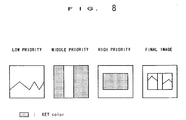
- Fig. 8 is an explanatory diagram showing a chromakey process, according to the invention.
- Fig. 9A is a block diagram showing a cellophane function according to the invention.
- Fig. 9B is a table showing data chroinakey processes of the VDP unit, control unit and image data extension unit, according to the invention.
- Fig. 10 is a flow chart showing operation of the cellophane function, according to the invention.
- Fig. 11 is an explanatory diagram showing the cellophane function, according to the invention.
- Fig. 12 is an explanatory diagram showing a front cellophane function, according to the invention.
- Fig. 13 is an explanatory diagram showing a back cellophane function, according to the invention.
- Figs. 14 to 16 and 18 to 25 are diagrams showing the configurations of an address register, status register, control register, color pallet address register, color pallet data write register, color pallet address offset register 1, color pallet address offset register 2, color pallet address offset register 3, color pallet address offset register 4 and two priority registers, respectively, according to the invention.
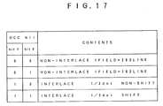
- Fig. 17 is a table showing information on the interlace and non-interlace modes, according to the invention.
- Figs. 26 to 28 are diagrams showing the configurations of chromakey-Y, chromakey-U and chromakey-V registers, respectively, according to the invention.
- Fig. 29 is a diagram showing the configuration of a fixed color register, according to the invention.
- Fig. 30 is a diagram showing the configuration of a cellophane image setting register, according to the invention.
- Figs. 31 to 37 are diagrams showing detail of the cellophane image setting register, shown in Fig. 30.
- Fig. 38 is a diagram showing the configuration of a special cellophane setting register, according to the invention.
- Fig. 39 is a diagram showing the configuration of a cellophane coefficient register, according to the invention.
- Fig. 40 is a diagram illustrating an image displayed in the non-interlace mode, according to the invention.
- Fig. 41 is a diagram illustrating an image displayed in an interlace mode, according to the invention.
- Fig. 42 is a diagram illustrating an image displayed in the interlace + 1/2 dot shift mode, according to the invention.
- Fig. 2 shows a computer system of the preferred embodiment.
- the system includes a game-software recording medium 100 such as a CD-ROM, a CPU 102 of 32-bit type, a control unit 104 for mainly controlling transmission of image and sound data and interfacing most devices to each other, an image data extension unit 106, an image data output unit 108, a sound data output unit 110, a video encoder unit 112, a VDP unit 114 and a TV display 116.
- CPU 102, control unit 104, image data extension unit 106 and VDP unit 114 are provided with their own memories K-RAM, M-RAM, R-RAM and V-RAM, respectively.
- CPU 102 directly controls a DRAM via a memory support, and performs communication through an I/O port to peripheral devices, that is, an I/O control function.
- CPU 102 includes a timer, a parallel I/O port and a interruption control system.
- VDP unit 114 reads display data which have been stored in the VRAM by CPU 102. The display data are transmitted to video encoder unit 112 whereby the data are displayed on the TV display 116.
- Control unit 104 includes an SCSI controller to which image and sound data are supplied from CD-ROM 100 through an SCSI interface. Data supplied to the SCSI controller is buffered in the K-RAM. Control unit 104 also includes a DRAM controller for reading data which have been buffered in the K-RAM, at a predetermined timing. In control unit 104, priority judgement is carried out for each dot of natural background image data, and an output signal is transmitted to video encoder unit 112.
- Control unit 104 transmits moving image data (full color, pallet), which has been reduced, to image data extension unit 106 whereby the scale-down data are extended.
- the extended data are transmitted from image data extension unit 106 to video encoder unit 112.
- Video encoder unit 112 superimposes VDP image data, natural background image data and moving image data (full color, pallet) transmitted from VDP unit 114, control unit 104 and image data extension unit 108, respectively. Video encoder unit 112 performs color pallet reproducing, special effect processing, D/A converting and the like. Output data of video encoder unit 112 are encoded into an NTSC signal by an external circuit.
- ADPCM sound data which have been recorded in CD-ROM 100 are buffered in the K-RAM and then transmitted to sound data output unit 110 by control unit 104.
- the sound data are reproduced by sound data output unit 110.
- Fig. 3 shows the video encoder unit, which is composed of an IC including a synchronizing signal generating circuit, a color pallet RAM, a priority arithmetic circuit, a cellophane arithmetic circuit (for synthesizing upper and lower pictures), a D/A converter for an image signal, an 8/16 bit data bus (M-bus) interface, a VDP interface, a control unit interface and an image data extension unit interface.
- an IC including a synchronizing signal generating circuit, a color pallet RAM, a priority arithmetic circuit, a cellophane arithmetic circuit (for synthesizing upper and lower pictures), a D/A converter for an image signal, an 8/16 bit data bus (M-bus) interface, a VDP interface, a control unit interface and an image data extension unit interface.
- M-bus 8/16 bit data bus
- the 8/16 bit data bus interface is an I/F switching circuit which selects one from 8 and 16 bit data buses to be used for data processing at the video encoder unit side. The selection is carried out in accordance with data width of the data bus of the processing system including the CPU.
- the VDP interface receives data transmitted from two of upper and lower VDPs. Normally, the VDP interface receives data from the upper VDP. The VDP interface receives data from the lower VDP only when the upper VDP supplies chromakey data.
- the color pallet RAM transforms a video input signal into a YUV digital signal.
- the video encoder unit has registers (16 bits ⁇ 24 lines), which are accessed by the CPU to set an operation mode therein, and to specify read and write modes for the color pallet.
- the color pallet RAM transforms color pallet data into YUV data to be actually displayed, as mentioned before.
- the color pallet RAM includes a color information table divided into 512 address regions each having one color and 16 bit data regions. Each color data are composed of 8 bits “Y", 4 bits “U” and 4 bits “V”, so that 65536 colors may be available.
- the "Y” data indicate brightness in a range 00 (black) to FF (white)
- the "U” data indicate color difference for a blue-to-yellow family in a range 0 to 15
- the "V” data indicate color difference for a red-to-green family in a range 0 to 15.
- the contents of the color pallet RAM are formed by the CPU, and are read in accordance with color pallet information from the VDP, control unit and image data extension unit.
- the read data are transformed into the Y, U and V data.
- the CPU can read the contents of the color pallet RAM.
- the data are written in the color pallet RAM continuously in accordance with the following steps:
- data are written in the data write register in the order of lower to upper bytes. After the upper bytes data are written in the data write register, the data are written in an internal register, and the CPA is incremented.
- the color pallet data stored in the VDP, control unit and image data extension unit are transformed to the YUV data in accordance with the contents of the color pallet RAM to form an actual image. All screens using the color pallet data are treated by the common color pallet RAM because only one color pallet RAM is provided. If a color pallet address offset register is used, color pallet start addresses may be specified for each picture separately.
- a picture to be displayed is specified for each dot. If the specified picture is a color pallet data picture, a color pallet address offset value of the picture is read from the register. After that, double the offset value is added to the color pallet data to provide a color pallet address. In accordance with the color pallet address, the color data Y, U and V are generated for each dot, and are transmitted to the following stage.
- the VDP has only one color pallet offset register, so that if plural VDPs are used, the plural VDPs have to use the single register in common. If the color pallet address is over 511, the tenth bit is omitted, that is, the ninth bit is connected to 0 address, as shown in Fig. 5. When the CPU accesses the color pallet RAM directly, the color pallet address offset is not effective.
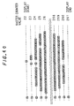
- Fig. 16 shows the contents of color pallet data transmitted from each of the LSIs.
- a pallet bank number is treated as the first bits of a pallet number, that is, the pallet and pallet bank numbers are not distinguished from each other. Therefore, all 8 bits data in each mode are treated as the color pallet data.
- the VDP unit treats two kinds images of the sprite (SP) and background (BG), the control unit treats four images BMG0, BMG1, BMG2 and BMG3, and the image data extension unit treats an IDCT/RL image, respectively.
- the video encoder unit may be connected with the upper and lower VDPs. If both the upper and lower VDPs are connected to the video encoder, one of the VDPs is selected to be connected at an input interface portion. The upper VDP is generally selected and the lower VDP is selected only when the upper VDP supplies chromakey data.
- the priority order of the SP and BG images of the VDP and the pictures BMG0 to BMG3 can not be changed only by the priority register of the video encoder unit. Therefore, if the priority order is changed, all the units must be changed.
- the priority order is decided for each dot by the video encoder unit in accordance with image information, the value of the priority register, whether the color is chromakey, and the like, the image information being transmitted from the VDP, control unit and image data extension unit.
- Fig. 7 shows priority processing in the 256 dots mode.
- the priority process is carried out using a clock of four times the dot clock, in addition to special processes such as the chromakey process and cellophane process.
- special processes such as the chromakey process and cellophane process.
- cellophane process upper and lower pictures (front and back cellophane) are synthesized when the video encoder synthesizes some images in accordance with the priority.
- each of the control unit and image data extension unit has 256 dots and the VDP has 320 dots. Therefore, an image to be displayed is specified in the period of 21MHz and the image (device) is displayed immediately.
- chromakey function transmission process
- some portions of an image are treated as transparency portions, on which low priority pictures are displayed.
- a color to be judged as a transparency is defined in advance.
- the key color differs depending on the type of data, color pallet data, IDCT-YUV data or YUV data of the control unit.
- To use no chromakey function is equivalent to use no key color when a picture to be displayed is drafted.
- Fig. 8 shows operation of the chromakey function. If a color pallet data 0 (pallet number 0 in VDP) is used as the key color, the color pallet data 0 is treated as a transparency color at the run-length region in the control unit and image data extension unit in any mode. In the VDP, regions of pallet number 0 are treated as transparency at any color pallet bank.
- Figs. 9A and 9B show the above mentioned chromakey operation.
- the control unit performs chromakey judgement and supplies an invalid signal to the color pallet data picture. If Y-data of YUV data are set "00h" on a dot in the control unit (in the 16M color mode and 64K color mode), the dot is displayed with transparency color independently of values for U and V data. A value of "01h” or the like is added to the Y-data at regions not to be displayed with transparency in order that the Y-data does not have a value "00h".
- an intermediate color located between a chromakey highest register value and a chromakey lowest register value is selected as the key color for the IDCT-YUV data screen and all of the YUV values to be displayed are located between the two register values, the selected color is judged as the key color, and as a result, the region is displayed with transparency color.
- the highest and lowest values of the chromakey Y register are Yu and Yl
- the highest and lowest values of the chromakey U register are Uu and Ul
- the highest and lowest values of the chromakey V register are Vu and Vl and Y
- U and V values to be displayed are Ys
- the dots corresponding to the invalid signals are treated the same as the case of key color, that is, the dots are displayed with transparency color.
- the chromakey portion on the lowest priority region is displayed with a color which will be used for the following portion in accordance with the priority process. Therefore, the following picture is displayed instead of the present one if all pictures including YUV data pictures are transparency. In the same manner, the chromakey region on the lowest priority picture is cellophane processed.
- Fig. 10 shows the cellophane function, which is for superimposing upper and lower pictures in accordance with the priority information stored in the video encoder.
- a lower priority picture is mixed with the 0 picture, so that the 0 picture is displayed with half-transparency color. It is possible to realize fade-in processing, fade-out processing and smoothly changing of pictures by varying the mix ratio of the cellophane function.
- the cellophane coefficient may be divided into 9, 0/8 to 8/8 so that the cellophane coefficient may be varied by changing the numerator.
- the cellophane coefficient is established by certain software.
- a cellophane coefficient register is provided with 3 regions each having 6 parameters.
- the cellophane function is set to a certain picture, the cellophane coefficient number (1 to 3) is written in a specified portion of the register. If "0" is set at the specified portion, the picture is separated from the cellophane function. Values 9 to F for the cellophane coefficient register are not supported.
- the cellophane arithmetic is not carried out to a chromakey portion of a picture to be overlapped with another picture, so that the general chromakey process is carried out to the overlapped picture.
- the cellophane function it is possible to realize functions of multi-cellophane, front cellophane, back cellophane and sprite special.
- the multi-cellophane function the cellophane process is carried out again on a picture which has been processed by the cellophane function.
- the front cellophane function the whole screen is changed in color and in brightness by the cellophane function using a pre-selected color.
- the cellophane process can be carried out on a picture having the lowest priority.
- the sprite special process the cellophane function can be used on the sprite picture for each pallet bank.
- the cellophane function on the sprite image may be controlled ON and OFF in accordance with a pallet bank number of the sprite image. That is, the cellophane arithmetic operation may be controlled for each pallet bank number.
- the cellophane process is carried out for each dot, as shown in Fig. 11.
- the VDP unit, control unit and image data extension unit supply first to third pictures I to III, the correspondence being arranged for each dot in accordance with picture priorities supplied from the units.
- the third picture III is used for the VDP unit
- the second picture II is used for the control unit
- the first picture I is used for the image data extension unit, respectively.
- the cellophane instruction is set on the second picture II (for example, the BMG1 picture of the control unit)
- the cellophane process is carried out on the first and second pictures I and II in accordance with the cellophane coefficient, which corresponds to the value set in the coefficient register of the second picture II.
- the cellophane instruction is set on the third picture III (for example, the BG picture)
- the cellophane process is carried out on the third picture III and the picture which has been cellophane processed between the first and second pictures I and II.
- the cellophane instruction is not set on the second picture II only, the cellophane process is carried out between the second and third pictures II and III because the first picture I is blinded by the second picture II.
- the second picture II does not blind the first picture at its chromakey portion. In this case, even if the cellophane instruction is set on the first picture I, the function is invalid.
- the cellophane instruction is set on and off dot-by-dot for each picture.
- each of the VDP and control unit supplies one dot data of one picture selected in accordance with its internal priority, so that the cellophane process can not be carried out between two pictures in the same device.
- cellophane arithmetic is performed between a selected picture and a fixed color picture having single color.
- the color of the fixed color picture is set at the fixed color register.
- a picture having the lowest priority picture selected from among pictures in the VDP unit, control unit and image data extension unit is cellophane processed with the fixed color picture, as shown in Fig. 13. Then the second lowest priority picture is cellophane processed in the same manner as the lowest priority picture.
- a value of the coefficient register set for the first picture is used as the cellophane coefficient.
- the front and back cellophane processes can not be carried out at the same time. Settings for front and back cellophane process are effective from the following horizontal synchronization period.
- All sprites in the VDP are recognized as sprite pictures, so that the all sprites are cellophane processed basically when the cellophane instruction is set on the sprite picture.
- specific sprites are not cellophane processed by the following method.
- dots in the specific sprite are treated as in a condition that the cellophane instruction is set on the specific sprite picture. This function is useful only when the cellophane arithmetic is carried out on the sprite picture. Therefore, if the cellophane instruction is set on a picture having a priority higher than that of the sprite picture, any sprite picture is cellophane processed.
- the video encoder unit contains a synchronizing signal generating circuit, so that a dot clock, horizontal synchronizing signals -HSYNCA, -HSYNCB and -HSYNCC and a vertical synchronizing signal -VSYNC are supplied to peripheral devices when a chrominance subcarrier frequency of 12 colors is supplied to the encoder unit.
- the synchronizing signal generating circuit has an external synchronizing function, that is, an image can be displayed in synchronization with an external image.
- a YUV signal of 8 bits is converted into an analog signal. If a UV signal contains only 4 bits like pallet data, "0000" data are added to the last figure of the UV signal to make it 8 bit data.
- the Y data are converted into an analog signal in linear fashion, for example, "00h” data are converted to a black color signal and "FFh” data are converted to a white color signal.
- the U and V data are also converted to analog signals in linear fashion.
- over and under "80h" data are expressed as positive and negative, respectively, because the U and V data have polarities.
- the color depth varies in series with the difference value from "80h.” When the data is "00h” or "FFh,” the color becomes the deepest. When both the U and V are “80h,” no color is expressed.
- the color hue is defined by the ratio between the difference values of the U and V signals from "80h,” and the polarities thereof.
- the D/A conversion process it may be selected whether the Y signal is treated with a synchronizing signal, and whether the U and V signals are modulated by chrominance subcarrier. If the clirominance subcarrier modulation is selected, color burst is superimposed on the U signal at a predetermined timing and amplitude.
- the D/A converter is of a current adding type, that is, a voltage conversion is carried out in accordance with the input impedance of external circuits.
- an RGB signal is generated.
- a composite video signal for the CRT display monitor is generated.
- Figs. 14 to 16 show the arrangements of an address register, the status register and a control register in the video encoder unit, respectively.
- the status and control registers are indirectly accessed through the address register.
- the address register (AR) specifies internal registers R00 to R15 in the video encoder unit.
- the status register holds the current information of the displayed image.
- control register (CR : R00)
- the 8th to 14th bits and the others are available from the following horizontal and vertical periods, respectively.
- Step 1 -CET (chip enable) and A1 terminals are set at "L" whereby the address register (AR) is accessed. Then, a register number of a register to be accessed next is written in the address register.
- Step 2 Then, the A1 terminal is changed to "H” while the -CET terminal keeps “L” whereby the register written in the address register is selected. Then, predetermined data are written into or read from the selected register.
- the content of the address register is maintained at the current value until the address register is rewritten. Therefore, the first step may be omitted when the same register is again accessed.
- the status register holds information such as the raster count value and interlace state.
- the data bus to be used is selected between 8 and 16 bit types by an EX8/-16 terminal. While the 8 bit type is used, lower and upper bytes of the register are accessed by setting an A0 terminal at "0" and "1", respectively. On the other hand, while the 16 bit type is used, the level at the A0 terminal is ignored, because 16 bits data can be accessed directly.
- Figs. 18 to 25 show the configurations of a color pallet address register, color pallet data write register, color pallet address offset register 1, color pallet address offset register 2, color pallet address offset register 3, color pallet address offset register 4, priority register 1, and priority register 2, respectively.
- the color pallet address register (CPA : R01) holds a color pallet address to be used when the color pallet RAM is accessed by the CPU, as shown in Fig. 18.
- the color pallet data write register and color pallet data read register are accessed in accordance with the color pallet address held in the color pallet address register.
- the color pallet address register is automatically incremented each time after the color pallet data write and read registers are accessed.
- the color pallet data write register (CPW : 02) holds YUV data to be written at the address CPA in the color pallet RAM by the CPU, as shown in Fig. 19.
- Each of the Y, U, and V data are indicated by positive whole numbers.
- Each of the U and V data are treated as 8 bits data by adding "0000" at the end thereof, because the D/A converter treats 8 bits data only.
- the writing process may carried out continuously by the automatic increment function of the color pallet address register.
- the writing process is carried out in the order of the last half bytes to the first half bytes, because the data are written in the register after the writing process for the first half data is carried out.
- the increment process of the CPA is also carried out after the first half data are written in the register.
- the color pallet data read register (CPR : R03) holds YUV data to be read from the color pallet RAM by the CPU.
- the reading process may carried out continuously by the automatic increment function of the color pallet address register.
- the reading process is carried out in the order of the last half bytes to the first half bytes, because the increment process is carried out after the first half data are read out.
- the color pallet address offset register 1, shown in Fig. 20, is used for specifying which color pallet is used first for each unit of the VDP pictures. Actually, a double value of that held in the register is used as the offset value for the color pallet address.
- the color pallet address offset register 2 shown in Fig. 21, is used for specifying which color pallet is used first for each unit of the image pictures supplied from the control unit.
- offset values are set for BM0 and BM1, respectively.
- BMG0 color pallet address BMG0 color pallet data + (BMG0 color pallet offset) ⁇ 2
- BMG1 color pallet address BMG1 color pallet data + (BMG1 color pallet offset) ⁇ 2
- the color pallet address offset register 3 shown in Fig. 22, is also used for specifying which color pallet is used first for each of the image pictures supplied from the control unit.
- offset values are set for BM2 and BM3, respectively.
- BMG2 color pallet address BMG2 color pallet data + (BMG2 color pallet offset) ⁇ 2
- BMG3 color pallet address BMG3 color pallet data + (BMG3 color pallet offset) ⁇ 2
- the color pallet address offset register 4, shown in Fig. 23, is used for specifying which color pallet is used first for each run-length picture supplied from the image data extension unit.
- the address offset value is effective from the following horizontal display period.
- the color pallet address run-length color pallet data + (run-length color pallet offset) ⁇ 2
- the priority registers 1 and 2 shown in Figs. 24 and 25, hold data of 3 bits for specifying priority orders of image pictures to be displayed. In these registers, a larger figure has higher priority and a lower figure has lower priority. The same figure is not allowed to be set in the different registers.
- Figs. 26 to 28 show chromakey-Y, chromakey-U and chromakey-V registers for the IDCT screen, respectively.
- the chromakey-Y (brightness) register shown in Fig. 26, stores data for specifying the upper and lower limits of a Y component in the chromakey function. In this register, "00H" and "FFH” represent black and white, respectively, these data being effective from the next horizontal display period.
- the chromakey-U (color difference) register shown in Fig. 27, stores data for specifying the upper and lower limits of a U component in the chromakey function. In this register, set data are effective from the next horizontal display period.
- the chromakey-V (color difference) register shown in Fig. 28, stores data for specifying the upper and lower limits of a U component in the chromakey function. In this register, set data are effective from the next horizontal display period.
- Fig. 29 shows a fixed color register (CCR : R0D), which is used for the front and back cellophane processing.
- the register stores Y data of 8 bits, U data of 4 bits and V data of 4 bits to specify a color, the data being set by the positive whole numbers. In this register, set data are effective from the next horizontal display period.
- Fig. 30 shows a cellophane setting register (BLE : ROE), in which set data are effective from the next horizontaldisplay period.
- BLE cellophane setting register
- Fig. 31 to 37 show detail of the cellophane setting register, shown in Fig. 30.
- Fig. 38 shows an SP cellophane setting register (SPBL : R0F).
- SPBL SP cellophane setting register
- a sprite picture using the color pallet bank is not processed by the cellophane function.
- This register is effective only when a cellophane ON is set for the sprite picture in the cellophane setting register.
- Fig. 39 shows a cellophane coefficient register, in which three pairs of data (1A, 1B), (2A, 2B) and (3A, 3B) are used. Each of Y, U and V data are divided into 9, “0/8" to "8/8,” so that the coefficient may be varied by changing the numerator.
- the priority processing is performed for each unit of predetermined dots, and therefore, plural pictures which are composed of different numbers of dots may be superimposed on each other. Further, this system may use the cellophane and chromakey processing together with the priority function, and as a result, high performance image processing may be realized.
- a cellophane coefficient register is provided with 3 regions each having 6 parameters.
- the cellophane function is set to a certain picture, the cellophane coefficient number (1 to 3) is written in a specified portion of the register. If "0" is set at the specified portion, the picture is separated from the cellophane function. Values 9 to F for the cellophane coefficient register are not supported.
- Fig. 40 shows image displayed in the non-interlace mode
- Figs. 41 and 42 show images displayed in a general interlace mode and in the interlace mode with a 1/2 dot shift function, which will be explained later.
- the video encoder may select an interlace mode, which is used for TV in general, and a non-interlace mode.
- the interlace mode scanning lines are fixed in number at 263 or 262, an O/E bit at a status register is "1" in an odd field period in first 1/60 seconds so that an image is displayed as in the non-interlace mode.
- an O/E bit becomes "0" to display an image located 1/2 line above the previous image.
- the distance between the first (odd) field and second (even) fields becomes narrow, and the image is displayed smoothly.
- these processes are repeated alternatively. If the odd and even fields have the same pictures, the image is displayed as if it seems being vibrated up and down with short interval. Image data are displayed field by field whereby the desired image is obtained.
- the 1/2 dot shift function In the interlace mode, it is possible to display a more higher quality image by using the 1/2 dot shift function therewith.
- the 1/2 dot shift function picture elements are shifted 1/2 dot in a horizontal direction at one line interval.
- a mask is used for smoothing notched edge lines of the image, so that the displayed image is composed of 255.5 dots.
Applications Claiming Priority (12)
| Application Number | Priority Date | Filing Date | Title |
|---|---|---|---|
| JP28515692A JPH06180569A (ja) | 1992-09-30 | 1992-09-30 | 画像処理装置 |
| JP28515792 | 1992-09-30 | ||
| JP28515692 | 1992-09-30 | ||
| JP285156/92 | 1992-09-30 | ||
| JP285157/92 | 1992-09-30 | ||
| JP4285157A JP2582743B2 (ja) | 1992-09-30 | 1992-09-30 | 画像処理装置 |
| JP29806992A JPH06295171A (ja) | 1992-10-09 | 1992-10-09 | 画像処理装置 |
| JP29806992 | 1992-10-09 | ||
| JP298069/92 | 1992-10-09 | ||
| JP30067192 | 1992-10-14 | ||
| JP300671/92 | 1992-10-14 | ||
| JP4300671A JPH06181579A (ja) | 1992-10-14 | 1992-10-14 | 画像処理装置 |
Publications (3)
| Publication Number | Publication Date |
|---|---|
| EP0590961A2 true EP0590961A2 (fr) | 1994-04-06 |
| EP0590961A3 EP0590961A3 (fr) | 1994-12-21 |
| EP0590961B1 EP0590961B1 (fr) | 2001-07-04 |
Family
ID=27479364
Family Applications (1)
| Application Number | Title | Priority Date | Filing Date |
|---|---|---|---|
| EP93307731A Expired - Lifetime EP0590961B1 (fr) | 1992-09-30 | 1993-09-29 | Appareil de traitement d'image |
Country Status (5)
| Country | Link |
|---|---|
| US (1) | US5467442A (fr) |
| EP (1) | EP0590961B1 (fr) |
| CA (1) | CA2107315A1 (fr) |
| DE (1) | DE69330397T2 (fr) |
| TW (1) | TW250555B (fr) |
Cited By (4)
| Publication number | Priority date | Publication date | Assignee | Title |
|---|---|---|---|---|
| US7136835B1 (en) | 1998-03-25 | 2006-11-14 | Orbis Patents Ltd. | Credit card system and method |
| US7433845B1 (en) | 1999-04-13 | 2008-10-07 | Orbis Patents Limited | Data structure, method and system for generating person-to-person, person-to-business, business-to-person, and business-to-business financial transactions |
| US7840486B2 (en) | 1999-01-15 | 2010-11-23 | D Agostino John | System and method for performing secure credit card purchases |
| US10592901B2 (en) | 2001-06-04 | 2020-03-17 | Orbis Patents, Ltd. | Business-to-business commerce using financial transaction numbers |
Families Citing this family (18)
| Publication number | Priority date | Publication date | Assignee | Title |
|---|---|---|---|---|
| DE69328399T2 (de) * | 1992-09-30 | 2000-10-19 | Hudson Soft Co Ltd | Sprachdaten-Verarbeitung |
| US5949919A (en) * | 1995-10-05 | 1999-09-07 | Microsoft Corporation | Precompression extrapolation method |
| US5787203A (en) * | 1996-01-19 | 1998-07-28 | Microsoft Corporation | Method and system for filtering compressed video images |
| US5799113A (en) * | 1996-01-19 | 1998-08-25 | Microsoft Corporation | Method for expanding contracted video images |
| US5764814A (en) * | 1996-03-22 | 1998-06-09 | Microsoft Corporation | Representation and encoding of general arbitrary shapes |
| US5778098A (en) * | 1996-03-22 | 1998-07-07 | Microsoft Corporation | Sprite coding |
| TW348239B (en) * | 1996-06-28 | 1998-12-21 | Cirrus Logic Inc | Embedding a transparency enable bit as part of a resizing bit block transfer operation |
| US6075875A (en) * | 1996-09-30 | 2000-06-13 | Microsoft Corporation | Segmentation of image features using hierarchical analysis of multi-valued image data and weighted averaging of segmentation results |
| US5748789A (en) * | 1996-10-31 | 1998-05-05 | Microsoft Corporation | Transparent block skipping in object-based video coding systems |
| US6917371B1 (en) * | 1996-11-22 | 2005-07-12 | Kabushiki Kaisha Sega Enterprises | Game device, picture data forming method and medium |
| US6400831B2 (en) | 1998-04-02 | 2002-06-04 | Microsoft Corporation | Semantic video object segmentation and tracking |
| JP4580738B2 (ja) * | 2004-11-22 | 2010-11-17 | オリンパスイメージング株式会社 | 電子機器 |
| JP2008228168A (ja) * | 2007-03-15 | 2008-09-25 | Fuji Xerox Co Ltd | 画像処理装置およびプログラム |
| US8149285B2 (en) * | 2007-09-12 | 2012-04-03 | Sanyo Electric Co., Ltd. | Video camera which executes a first process and a second process on image data |
| JP5030822B2 (ja) * | 2008-03-07 | 2012-09-19 | 三洋電機株式会社 | 電子カメラ |
| TWI542264B (zh) | 2010-12-24 | 2016-07-11 | Lg伊諾特股份有限公司 | 印刷電路板及其製造方法 |
| US9872005B2 (en) | 2014-01-21 | 2018-01-16 | Mitsubishi Electric Corporation | Moving image reproducing apparatus |
| CN112822973A (zh) | 2018-10-10 | 2021-05-18 | 佳能株式会社 | 医学图像处理装置、医学图像处理方法和程序 |
Citations (3)
| Publication number | Priority date | Publication date | Assignee | Title |
|---|---|---|---|---|
| EP0171120A1 (fr) * | 1984-08-10 | 1986-02-12 | Rtc-Compelec | Procédé et dispositif pour créer et modifier une image synthetique |
| EP0309373A2 (fr) * | 1987-09-21 | 1989-03-29 | International Business Machines Corporation | Animation interactive d'objets graphiques |
| WO1991018359A1 (fr) * | 1990-05-12 | 1991-11-28 | Rediffusion Simulation Limited | Generateur d'images |
Family Cites Families (1)
| Publication number | Priority date | Publication date | Assignee | Title |
|---|---|---|---|---|
| US4704605A (en) * | 1984-12-17 | 1987-11-03 | Edelson Steven D | Method and apparatus for providing anti-aliased edges in pixel-mapped computer graphics |
-
1993
- 1993-09-08 TW TW082107337A patent/TW250555B/zh active
- 1993-09-29 DE DE69330397T patent/DE69330397T2/de not_active Expired - Fee Related
- 1993-09-29 US US08/128,285 patent/US5467442A/en not_active Expired - Fee Related
- 1993-09-29 EP EP93307731A patent/EP0590961B1/fr not_active Expired - Lifetime
- 1993-09-29 CA CA002107315A patent/CA2107315A1/fr not_active Abandoned
Patent Citations (3)
| Publication number | Priority date | Publication date | Assignee | Title |
|---|---|---|---|---|
| EP0171120A1 (fr) * | 1984-08-10 | 1986-02-12 | Rtc-Compelec | Procédé et dispositif pour créer et modifier une image synthetique |
| EP0309373A2 (fr) * | 1987-09-21 | 1989-03-29 | International Business Machines Corporation | Animation interactive d'objets graphiques |
| WO1991018359A1 (fr) * | 1990-05-12 | 1991-11-28 | Rediffusion Simulation Limited | Generateur d'images |
Cited By (13)
| Publication number | Priority date | Publication date | Assignee | Title |
|---|---|---|---|---|
| US8756150B2 (en) | 1998-03-25 | 2014-06-17 | Orbis Patents Limited | Credit card system and method |
| US7567934B2 (en) | 1998-03-25 | 2009-07-28 | Orbis Patents Ltd. | Credit card system and method |
| US7571142B1 (en) | 1998-03-25 | 2009-08-04 | Orbis Patents Limited | Credit card system and method |
| US7593896B1 (en) | 1998-03-25 | 2009-09-22 | Orbis Patents Ltd. | Credit card system and method |
| US8676707B2 (en) | 1998-03-25 | 2014-03-18 | Orbis Patents Ltd. | Credit cards system and method having additional features |
| US7136835B1 (en) | 1998-03-25 | 2006-11-14 | Orbis Patents Ltd. | Credit card system and method |
| US9881298B2 (en) | 1998-03-25 | 2018-01-30 | Orbis Patents Limited | Credit card system and method |
| US9898730B2 (en) | 1998-03-25 | 2018-02-20 | Orbit Patents Limited | Credit card system and method |
| US7840486B2 (en) | 1999-01-15 | 2010-11-23 | D Agostino John | System and method for performing secure credit card purchases |
| US8036988B2 (en) | 1999-01-15 | 2011-10-11 | D Agostino John | System and method for performing secure credit card transactions |
| US7433845B1 (en) | 1999-04-13 | 2008-10-07 | Orbis Patents Limited | Data structure, method and system for generating person-to-person, person-to-business, business-to-person, and business-to-business financial transactions |
| US7895122B2 (en) | 1999-04-13 | 2011-02-22 | Orbis Patents Limited | Person-to-person, person-to business and business-to-business financial transaction system |
| US10592901B2 (en) | 2001-06-04 | 2020-03-17 | Orbis Patents, Ltd. | Business-to-business commerce using financial transaction numbers |
Also Published As
| Publication number | Publication date |
|---|---|
| DE69330397D1 (de) | 2001-08-09 |
| EP0590961B1 (fr) | 2001-07-04 |
| CA2107315A1 (fr) | 1994-03-31 |
| US5467442A (en) | 1995-11-14 |
| EP0590961A3 (fr) | 1994-12-21 |
| TW250555B (fr) | 1995-07-01 |
| DE69330397T2 (de) | 2001-10-18 |
Similar Documents
| Publication | Publication Date | Title |
|---|---|---|
| EP0590961B1 (fr) | Appareil de traitement d'image | |
| US5125671A (en) | T.V. game system having reduced memory needs | |
| US5337069A (en) | Still picture display apparatus and external storage device used therein | |
| EP0473390B1 (fr) | Superposition d'images fixes formées des caractères | |
| US20010017613A1 (en) | Image processing system | |
| US6369827B1 (en) | Method and apparatus for displaying higher color resolution on a hand-held LCD device | |
| EP0573294A1 (fr) | Dispositif pour enchainer un signal de reproduction vidéo avec un signal vidéo-graphique | |
| EP0590785B1 (fr) | Appareil de traitement de données de sons et d'images | |
| US5479604A (en) | Image processing apparatus which provides an indication of whether an odd or an even field is displayed | |
| JP3059302B2 (ja) | 映像混合装置 | |
| US7092585B2 (en) | Method and apparatus for processing both static and moving images | |
| US5781183A (en) | Image processing apparatus including selecting function for displayed colors | |
| CA2017600C (fr) | Appareil de superposition d'images matricielles a des signaux video | |
| US7050064B2 (en) | Method and apparatus for displaying higher color resolution on a hand-held LCD device | |
| JPH06180569A (ja) | 画像処理装置 | |
| US5426516A (en) | Color image processing apparatus | |
| EP0466935B1 (fr) | Dispositif d'affichage d'images immobiles et cartouche de memoire externe utilisee avec un tel dispositif | |
| JP2582743B2 (ja) | 画像処理装置 | |
| JPH027478B2 (fr) | ||
| EP0121810B1 (fr) | Microprocesseur | |
| KR880000993B1 (ko) | 고정패턴용 롬 사용방법 | |
| JPH06181579A (ja) | 画像処理装置 | |
| JPH06295171A (ja) | 画像処理装置 | |
| JP2000296229A (ja) | パチンコ機の画像処理表示装置 | |
| JPH0729031A (ja) | 画像合成装置 |
Legal Events
| Date | Code | Title | Description |
|---|---|---|---|
| PUAI | Public reference made under article 153(3) epc to a published international application that has entered the european phase |
Free format text: ORIGINAL CODE: 0009012 |
|
| AK | Designated contracting states |
Kind code of ref document: A2 Designated state(s): DE FR GB NL |
|
| PUAL | Search report despatched |
Free format text: ORIGINAL CODE: 0009013 |
|
| AK | Designated contracting states |
Kind code of ref document: A3 Designated state(s): DE FR GB NL |
|
| 17P | Request for examination filed |
Effective date: 19950526 |
|
| 17Q | First examination report despatched |
Effective date: 19981221 |
|
| RIC1 | Information provided on ipc code assigned before grant |
Free format text: 7G 06T 15/40 A |
|
| GRAG | Despatch of communication of intention to grant |
Free format text: ORIGINAL CODE: EPIDOS AGRA |
|
| GRAG | Despatch of communication of intention to grant |
Free format text: ORIGINAL CODE: EPIDOS AGRA |
|
| GRAH | Despatch of communication of intention to grant a patent |
Free format text: ORIGINAL CODE: EPIDOS IGRA |
|
| GRAH | Despatch of communication of intention to grant a patent |
Free format text: ORIGINAL CODE: EPIDOS IGRA |
|
| GRAA | (expected) grant |
Free format text: ORIGINAL CODE: 0009210 |
|
| AK | Designated contracting states |
Kind code of ref document: B1 Designated state(s): DE FR GB NL |
|
| REF | Corresponds to: |
Ref document number: 69330397 Country of ref document: DE Date of ref document: 20010809 |
|
| PG25 | Lapsed in a contracting state [announced via postgrant information from national office to epo] |
Ref country code: GB Free format text: LAPSE BECAUSE OF NON-PAYMENT OF DUE FEES Effective date: 20011004 |
|
| ET | Fr: translation filed | ||
| REG | Reference to a national code |
Ref country code: GB Ref legal event code: IF02 |
|
| PG25 | Lapsed in a contracting state [announced via postgrant information from national office to epo] |
Ref country code: NL Free format text: LAPSE BECAUSE OF NON-PAYMENT OF DUE FEES Effective date: 20020401 |
|
| PG25 | Lapsed in a contracting state [announced via postgrant information from national office to epo] |
Ref country code: DE Free format text: LAPSE BECAUSE OF NON-PAYMENT OF DUE FEES Effective date: 20020501 |
|
| PLBE | No opposition filed within time limit |
Free format text: ORIGINAL CODE: 0009261 |
|
| STAA | Information on the status of an ep patent application or granted ep patent |
Free format text: STATUS: NO OPPOSITION FILED WITHIN TIME LIMIT |
|
| GBPC | Gb: european patent ceased through non-payment of renewal fee |
Effective date: 20011004 |
|
| PG25 | Lapsed in a contracting state [announced via postgrant information from national office to epo] |
Ref country code: FR Free format text: LAPSE BECAUSE OF NON-PAYMENT OF DUE FEES Effective date: 20020531 |
|
| NLV4 | Nl: lapsed or anulled due to non-payment of the annual fee |
Effective date: 20020401 |
|
| 26N | No opposition filed | ||
| REG | Reference to a national code |
Ref country code: FR Ref legal event code: ST |
|
| NLV4 | Nl: lapsed or anulled due to non-payment of the annual fee |
Effective date: 20020401 |