EP0574635A1 - Méthode et appareil de détection et compensation de perte de signal - Google Patents
Méthode et appareil de détection et compensation de perte de signal Download PDFInfo
- Publication number
- EP0574635A1 EP0574635A1 EP92401669A EP92401669A EP0574635A1 EP 0574635 A1 EP0574635 A1 EP 0574635A1 EP 92401669 A EP92401669 A EP 92401669A EP 92401669 A EP92401669 A EP 92401669A EP 0574635 A1 EP0574635 A1 EP 0574635A1
- Authority
- EP
- European Patent Office
- Prior art keywords
- ampl
- dropout
- signal
- compensation
- circuit
- Prior art date
- Legal status (The legal status is an assumption and is not a legal conclusion. Google has not performed a legal analysis and makes no representation as to the accuracy of the status listed.)
- Granted
Links
- 238000000034 method Methods 0.000 title claims abstract description 26
- 238000001514 detection method Methods 0.000 title claims description 8
- 230000010354 integration Effects 0.000 claims description 4
- 238000012935 Averaging Methods 0.000 claims description 2
- 102100032187 Androgen receptor Human genes 0.000 claims 1
- 108091008581 nuclear androgen receptors Proteins 0.000 claims 1
- 230000005540 biological transmission Effects 0.000 abstract description 5
- 239000002131 composite material Substances 0.000 abstract description 5
- 230000000694 effects Effects 0.000 abstract description 3
- 238000006243 chemical reaction Methods 0.000 abstract description 2
- 101001005166 Homo sapiens Lens fiber membrane intrinsic protein Proteins 0.000 description 3
- 102100026038 Lens fiber membrane intrinsic protein Human genes 0.000 description 3
- 230000001419 dependent effect Effects 0.000 description 3
- 238000005070 sampling Methods 0.000 description 3
- 238000010586 diagram Methods 0.000 description 2
- 238000001914 filtration Methods 0.000 description 2
- 101001020548 Homo sapiens LIM/homeobox protein Lhx1 Proteins 0.000 description 1
- 101000976913 Homo sapiens Lens fiber major intrinsic protein Proteins 0.000 description 1
- 102100023487 Lens fiber major intrinsic protein Human genes 0.000 description 1
- 230000003044 adaptive effect Effects 0.000 description 1
- 230000006735 deficit Effects 0.000 description 1
- 230000036039 immunity Effects 0.000 description 1
- 230000010355 oscillation Effects 0.000 description 1
- 230000035945 sensitivity Effects 0.000 description 1
Images


Classifications
-
- H—ELECTRICITY
- H04—ELECTRIC COMMUNICATION TECHNIQUE
- H04N—PICTORIAL COMMUNICATION, e.g. TELEVISION
- H04N5/00—Details of television systems
- H04N5/14—Picture signal circuitry for video frequency region
- H04N5/21—Circuitry for suppressing or minimising disturbance, e.g. moiré or halo
-
- H—ELECTRICITY
- H04—ELECTRIC COMMUNICATION TECHNIQUE
- H04N—PICTORIAL COMMUNICATION, e.g. TELEVISION
- H04N5/00—Details of television systems
- H04N5/76—Television signal recording
- H04N5/91—Television signal processing therefor
- H04N5/93—Regeneration of the television signal or of selected parts thereof
- H04N5/94—Signal drop-out compensation
Definitions
- the present invention relates to a method and to an apparatus for dropout detection and compensation.
- the digitization of the analogue composite signal within the SECAM standard with 8 bits can pose serious problems for the chrominance signals as opposed to the digitization of NTSC or PAL signals. Due to the compatibility constraints given by the black and white TV sets in former times the amplitude of the FM subcarrier was chosen relatively small. This has led to an unfavourable signal-to-noise ratio for the chrominance signal compared with the other colour TV standards. This fact can give rise to unacceptable quantizing errors during the A/D conversion of the FM modulated chrominance signal, if the high frequency part of the composite signal has been subjected to a high degree of attenuation caused by mistuning effects in the receiver or not well adjusted frequency converter in the transmission chain, etc. In that case the reconstructed picture exhibits 'coloured fishes' (coloured FM spikes).
- the drop out compensation is made soft switch controlled at the output of the FM demodulator, whereby the input signal of the drop out detector is received from the input of the FM demodulator.
- this inventive method consists in dropout compensation of FM modulated video signals, whereby a dropout (DO) in a specific line (Ln) of a FM modulated component (D' R , D' B ) is compensated using the respective component from a neighboured line (Ln-2), and said compensation (DOC) is made for FM demodulated components (DOCI), whereby said dropout (DO) is detected (DOD) from said FM modulated component (FMS) and the amount of said compensation (DOC) is soft switch controlled ( ⁇ ) in accordance with a modulation amplitude (AMPL, AMPL ) of said FM modulated component (FMS).
- a dropout (DO) in a specific line (Ln) of a FM modulated component (D' R , D' B ) is compensated using the respective component from a neighboured line (Ln-2), and said compensation (DOC) is made for FM demodulated components (DOCI), whereby said dropout (DO) is detected (DOD) from said FM modulated component (FMS
- this inventive method consists in dropout detection of FM modulated video signals, whereby said dropout (DO) occurs in a specific line (Ln) of a FM modulated component (D' R , D' B ) and is compensated using the respective component from a neighboured line (Ln-2), whereby the current modulation amplitude (AMPL) of said FM modulated component and the amplitude ( AMPL ) of rest frequencies within a horizontal blanking period of said FM video signal is measured and a soft switch control signal ( ⁇ ) for controlling the amount of said compensation (DOC) of the FM demodulated video signal is generated in accordance with the ratio (AMPL/ AMPL ) between these amplitude values (AMPL, AMPL ).
- this inventive apparatus comprises a digital FM demodulator (FMD) and a succeeding soft switch controlled ( ⁇ ) dropout compensator (DOC) in which a dropout (DO) in a specific line (Ln) of a FM modulated component (D' R , D' B ) is compensated using the respective component from a neighboured line (Ln-2), whereby said dropout (DO) is detected in a dropout detector (DOD) from the input signal of said FM demodulator (FMD) and whereby the amount of said compensation is in accordance with the modulation amplitude (AMPL, AMPL ) of the input signal of said FM demodulator (FMD).
- DOD dropout detector
- this inventive apparatus comprises a FM demodulator (FMD) and a succeeding soft switch controlled ( ⁇ ) dropout compensator (DOC) and comprises an absolute value circuit (ABS) to which the input signal of said FM demodulator, sampled (f s ) with about four times the colour subcarrier frequency (f sc ), is fed and whose output is connected to: a mean square value circuit (MSV) for each two succeeding samples, whereby four of each succeeding mean square values are averaged in a second horizontal average circuit (HOAV2), whose output is used for determining the current modulation amplitude (AMPL); a horizontal integration circuit (HOI) in which a mean value of the rest frequencies amplitudes during the burst period is evaluated, gated by a back porch signal (BP), and averaged over each four TV lines in a vertical averager (VEAV); a first horizontal average circuit (HOAV1) for averaging each four samples, whose output is connected to a hold function circuit (HOI) in which, gated by a back
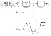
- Fig. 1a shows an arrangement within a digital SECAM decoder which can lead to the kind of distortion mentioned above.
- a coded SECAM TV signal is fed via input CSI to a clamp circuit CL and then passed through an A/D converter AD with a sampling frequency f s and a bandpass BP to a HF-deemphasis circuit HDE.
- a signal depicted in Fig. 1b is available.
- the FM burst FMB has a rather low amplitude. Where this burst is reduced due to e.g. transmission errors 'coloured fishes' CF will arise after demodulation in FM demodulator at output DSO.
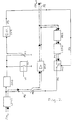
- Fig. 2 illustrates the block diagram of a conventional drop out compensator.
- the drop out compensator as shown in the Fig. 2 is located between the output of the VCR head amplifier and the input of the limiter prior to the FM demodulator.
- the principal behaviour can now be described as follows: A FM modulated input signal FMin is passed through a first limiter LIM1 as signal P2 to a drop out detector DOD and to a first potentiometer RB. Without the occurrence of any drop outs the FM signal passes along the broken line in Fig. 2.
- the FM signal is weighted by the potentiometer RB and goes into an emitter follower AMP before it will go as signal FMout (P5) to the input of a further limiter (not illustrated in Fig. 2) prior to a FM demodulator and to the input of the feed back loop.
- the feed back loop starts with a line delay (DEL) of 64 ⁇ s, is continued by a second limiter LIM2 and a gate SW2 which output is set by a control signal P3 to zero, if no drop out occurs.
- the drop out detector DOD generates an output signal different from zero which will be thresholded afterwards in a threshold circuit THR and used to close the feed back loop.
- the output signal of the drop out detector DOD is periodically connected to ground in a switch SW1 by vertical impulses VI.
- the threshold for signal P3 can be adjusted with a second potentiometer RS. If the output signal P3 of circuit THR is 'high', the output signal P1 of second limiter LIM2 is connected via gate SW2 to the other input signal P4 of the first potentiometer RB. This potentiometer allows then to adjust a balance between the FM input signal P2 and the feedback signal P4.
- Fig. 3 illustrates the behaviour of this circuit for a drop out DO within one TV line.
- the signals P1 to P5 correspond to the respective signals in Fig. 2:
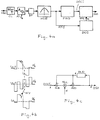
- Fig. 4a The input CSI, the output DSO and the circuits CL, AD, BP, HDE and FMD correspond to Fig. 1.
- the sampling frequency f s can be chosen to about four times the colour subcarrier frequency f sc .
- the drop out compensation circuit DOC is located after the FM demodulator FMD, whereby the input signal FMS of the drop out detector DOD comes from the input signal of the FM detector.
- the current chrominance signal at the output of the FM demodulator will be replaced REP by the signal of the previous line of the same chrominance component as shown in Fig.
- the drop out compensator comprises a feed back loop with a 128 ⁇ s delay DLD (because of the alternate-line scanned chrominance signals) and a soft switch between the input signal DOCI of the dropout compensator and the feed back signal as it is depicted in Fig. 4c.
- the soft switch can be arranged in the following way: The output of delay DLD is subtracted from input signal DOCI in a subtractor SUB and added in an adder ADD to the output of a multiplier MUL, whereby the output of the adder is connected to the input of the delay and the output of the subtractor is connected to a first input of the multiplier and a control signal ⁇ is fed to the other multiplier input.
- the soft switch control signal ⁇ is generated by the drop out detector DOD in which the current amplitude at the input of the FM demodulator is measured and in which different thresholds can be selected depending on the current burst amplitude retrieved at the beginning of each line.
- control signal ⁇ becomes '1' and the signal coming from the FM demodulator is passed through the compensator without manipulation.
- the control signal ⁇ will be forced to zero and the complete previous line of the same chrominance component will be repeated.
- this recursive structure is stable in any case, no oscillations can occur.
- the double line delay DLD in the feed back loop necessitates the full bandwidth.
- the drop out compensator DOC will fail, if the output signal of the FM demodulator FMD is subjected to video deemphasis, lowpass filtering and sub-sampling (not illustrated in Fig. 4) prior to the drop out compensation. This is mainly due to the dispersal of the sharp impulses at the FM demodulator output after the lowpass filtering.
- Fig. 5a A more complex processing is carried out within the drop out detector DOD, depicted in Fig. 5a, which can be split into two parts:
- the difference ⁇ is compared in a double threshold circuit DTHR with different preselected values C1, C2 and ⁇ c .
- ⁇ will also be small and the upper UT and lower LT threshold of the applied non-linearity have a minimum value.
- the parameters C1, C2 and ⁇ c represent empirical values which have proved to be suitable. If the amplitude AMPL falls below a certain threshold AMPL min the transfer characteristic ALAM of the non-linearity is advantageously kept constant.
- the drop out compensation technique has proved to be quite effective in suppressing 'coloured fishes'. Even for sequences for which the subcarrier is already unvisible in case when the composite signal is observed on the screen, the digital SECAM decoder exhibits a significantly improved colour reproduction.
- the invention can also be used to detect FM spikes after satellite transmission of SECAM signals and to compensate these distortions.
- the invention can also be used in digital transcoders from SECAM to other TV standards like PAL or NTSC.
Landscapes
- Engineering & Computer Science (AREA)
- Multimedia (AREA)
- Signal Processing (AREA)
- Television Signal Processing For Recording (AREA)
Priority Applications (2)
| Application Number | Priority Date | Filing Date | Title |
|---|---|---|---|
| DE1992627026 DE69227026T2 (de) | 1992-06-16 | 1992-06-16 | Verfahren und Gerät zur Erfassung und Kompensation von Signalausfällen |
| EP19920401669 EP0574635B1 (fr) | 1992-06-16 | 1992-06-16 | Méthode et appareil de détection et compensation de perte de signal |
Applications Claiming Priority (1)
| Application Number | Priority Date | Filing Date | Title |
|---|---|---|---|
| EP19920401669 EP0574635B1 (fr) | 1992-06-16 | 1992-06-16 | Méthode et appareil de détection et compensation de perte de signal |
Publications (2)
| Publication Number | Publication Date |
|---|---|
| EP0574635A1 true EP0574635A1 (fr) | 1993-12-22 |
| EP0574635B1 EP0574635B1 (fr) | 1998-09-16 |
Family
ID=8211671
Family Applications (1)
| Application Number | Title | Priority Date | Filing Date |
|---|---|---|---|
| EP19920401669 Expired - Lifetime EP0574635B1 (fr) | 1992-06-16 | 1992-06-16 | Méthode et appareil de détection et compensation de perte de signal |
Country Status (2)
| Country | Link |
|---|---|
| EP (1) | EP0574635B1 (fr) |
| DE (1) | DE69227026T2 (fr) |
Cited By (1)
| Publication number | Priority date | Publication date | Assignee | Title |
|---|---|---|---|---|
| CN106657978A (zh) * | 2016-08-31 | 2017-05-10 | 广州赛宝计量检测中心服务有限公司 | 一种用于视频信号分析仪校准的失真信号发生装置 |
Citations (2)
| Publication number | Priority date | Publication date | Assignee | Title |
|---|---|---|---|---|
| US4977461A (en) * | 1988-03-18 | 1990-12-11 | Sony Corporation | Dropout detecting circuit with one-half wavelength delay |
| WO1992006558A1 (fr) * | 1990-09-28 | 1992-04-16 | Thomson Consumer Electronics S.A. | Procede de mesure du bruit dans une image video active et dispositif pour la mise en ×uvre du procede |
-
1992
- 1992-06-16 EP EP19920401669 patent/EP0574635B1/fr not_active Expired - Lifetime
- 1992-06-16 DE DE1992627026 patent/DE69227026T2/de not_active Expired - Fee Related
Patent Citations (2)
| Publication number | Priority date | Publication date | Assignee | Title |
|---|---|---|---|---|
| US4977461A (en) * | 1988-03-18 | 1990-12-11 | Sony Corporation | Dropout detecting circuit with one-half wavelength delay |
| WO1992006558A1 (fr) * | 1990-09-28 | 1992-04-16 | Thomson Consumer Electronics S.A. | Procede de mesure du bruit dans une image video active et dispositif pour la mise en ×uvre du procede |
Non-Patent Citations (1)
| Title |
|---|
| IEEE TRANSACTIONS ON CONSUMER ELECTRONICS vol. 31, no. 3, August 1985, NEW YORK US pages 226 - 239 TEICHNER 'QUALITY IMPROVEMENT BY ADAPTIVE INTER-/INTRAFRAME PROCESSING IN PAL TV RECEIVERS' * |
Cited By (1)
| Publication number | Priority date | Publication date | Assignee | Title |
|---|---|---|---|---|
| CN106657978A (zh) * | 2016-08-31 | 2017-05-10 | 广州赛宝计量检测中心服务有限公司 | 一种用于视频信号分析仪校准的失真信号发生装置 |
Also Published As
| Publication number | Publication date |
|---|---|
| EP0574635B1 (fr) | 1998-09-16 |
| DE69227026T2 (de) | 1999-04-01 |
| DE69227026D1 (de) | 1998-10-22 |
Similar Documents
| Publication | Publication Date | Title |
|---|---|---|
| US5844629A (en) | Digital-to-analog video encoder with novel equalization | |
| US4050084A (en) | Comb filter for television signals having adaptive features | |
| CA1093205A (fr) | Circuit de separation des donnees de chrominance et de luminance d'un signal video composite | |
| CA2095435A1 (fr) | Systeme de telediffusion haute definition a boite de commande video avec interference reduite selon la norme ntsc | |
| CA1275727C (fr) | Systeme de traitement de signaux video brouilles | |
| KR19990007950A (ko) | 공통 지연 소자를 갖는 휘도/색차 분리필터 | |
| EP0212674B1 (fr) | Circuit de suppression de bruit avec commande de gain | |
| US4417270A (en) | Wide band chrominance demodulator with color noise reduction function | |
| US4532540A (en) | Teletext set-top converter with transparent mode | |
| JPS6148313B2 (fr) | ||
| US4430665A (en) | Automatic video signal peaking and color control | |
| US4480266A (en) | Method and apparatus for preventing generation of false color signals in color television cameras | |
| CA2043856C (fr) | Dispositif de correction de la tonalite des couleurs dans les signaux video | |
| US4775888A (en) | Motion detector for chrominance signal in TV receiver | |
| EP0574635B1 (fr) | Méthode et appareil de détection et compensation de perte de signal | |
| US4736252A (en) | Motion detector for chrominance signal in TV receiver | |
| US5223920A (en) | Video processor having automatic chrominance control compensation | |
| US6950149B1 (en) | Comb filter and a video apparatus | |
| US5294985A (en) | Signal limiting apparatus having improved spurious signal performance and methods | |
| US4646152A (en) | Sharpness enhanced equal bandwidth luminance bandwidth compression system | |
| US5432557A (en) | Extended television signal receiver | |
| JPH0638669B2 (ja) | 動き検出回路 | |
| US4758900A (en) | Field/frame conversion method for magnetic picture recording with demodulation, interpolation and de-emphasis after conversion | |
| US5187568A (en) | Video processor having improved clamping system for color television receivers | |
| JP2609657B2 (ja) | テレビジョン受信機 |
Legal Events
| Date | Code | Title | Description |
|---|---|---|---|
| PUAI | Public reference made under article 153(3) epc to a published international application that has entered the european phase |
Free format text: ORIGINAL CODE: 0009012 |
|
| AK | Designated contracting states |
Kind code of ref document: A1 Designated state(s): AT BE CH DE DK ES FR GB GR IT LI LU MC NL PT SE |
|
| RBV | Designated contracting states (corrected) |
Designated state(s): DE ES FR GB IT |
|
| 17P | Request for examination filed |
Effective date: 19940531 |
|
| RAP1 | Party data changed (applicant data changed or rights of an application transferred) |
Owner name: THOMSON MULTIMEDIA |
|
| 17Q | First examination report despatched |
Effective date: 19960710 |
|
| GRAG | Despatch of communication of intention to grant |
Free format text: ORIGINAL CODE: EPIDOS AGRA |
|
| GRAG | Despatch of communication of intention to grant |
Free format text: ORIGINAL CODE: EPIDOS AGRA |
|
| GRAH | Despatch of communication of intention to grant a patent |
Free format text: ORIGINAL CODE: EPIDOS IGRA |
|
| RAP1 | Party data changed (applicant data changed or rights of an application transferred) |
Owner name: THOMSON MULTIMEDIA |
|
| GRAH | Despatch of communication of intention to grant a patent |
Free format text: ORIGINAL CODE: EPIDOS IGRA |
|
| GRAA | (expected) grant |
Free format text: ORIGINAL CODE: 0009210 |
|
| AK | Designated contracting states |
Kind code of ref document: B1 Designated state(s): DE ES FR GB IT |
|
| PG25 | Lapsed in a contracting state [announced via postgrant information from national office to epo] |
Ref country code: IT Free format text: LAPSE BECAUSE OF FAILURE TO SUBMIT A TRANSLATION OF THE DESCRIPTION OR TO PAY THE FEE WITHIN THE PRE;WARNING: LAPSES OF ITALIAN PATENTS WITH EFFECTIVE DATE BEFORE 2007 MAY HAVE OCCURRED AT ANY TIME BEFORE 2007. THE CORRECT EFFECTIVE DATE MAY BE DIFFERENT FROM THE ONE RECORDED.SCRIBED TIME-LIMIT Effective date: 19980916 Ref country code: ES Free format text: THE PATENT HAS BEEN ANNULLED BY A DECISION OF A NATIONAL AUTHORITY Effective date: 19980916 |
|
| REF | Corresponds to: |
Ref document number: 69227026 Country of ref document: DE Date of ref document: 19981022 |
|
| ET | Fr: translation filed | ||
| PLBE | No opposition filed within time limit |
Free format text: ORIGINAL CODE: 0009261 |
|
| STAA | Information on the status of an ep patent application or granted ep patent |
Free format text: STATUS: NO OPPOSITION FILED WITHIN TIME LIMIT |
|
| 26N | No opposition filed | ||
| REG | Reference to a national code |
Ref country code: GB Ref legal event code: 746 Effective date: 20010810 |
|
| REG | Reference to a national code |
Ref country code: GB Ref legal event code: IF02 |
|
| REG | Reference to a national code |
Ref country code: FR Ref legal event code: D6 |
|
| PGFP | Annual fee paid to national office [announced via postgrant information from national office to epo] |
Ref country code: DE Payment date: 20070628 Year of fee payment: 16 |
|
| PGFP | Annual fee paid to national office [announced via postgrant information from national office to epo] |
Ref country code: GB Payment date: 20070511 Year of fee payment: 16 |
|
| PGFP | Annual fee paid to national office [announced via postgrant information from national office to epo] |
Ref country code: FR Payment date: 20070626 Year of fee payment: 16 |
|
| GBPC | Gb: european patent ceased through non-payment of renewal fee |
Effective date: 20080616 |
|
| REG | Reference to a national code |
Ref country code: FR Ref legal event code: ST Effective date: 20090228 |
|
| PG25 | Lapsed in a contracting state [announced via postgrant information from national office to epo] |
Ref country code: DE Free format text: LAPSE BECAUSE OF NON-PAYMENT OF DUE FEES Effective date: 20090101 |
|
| PG25 | Lapsed in a contracting state [announced via postgrant information from national office to epo] |
Ref country code: GB Free format text: LAPSE BECAUSE OF NON-PAYMENT OF DUE FEES Effective date: 20080616 |
|
| PG25 | Lapsed in a contracting state [announced via postgrant information from national office to epo] |
Ref country code: FR Free format text: LAPSE BECAUSE OF NON-PAYMENT OF DUE FEES Effective date: 20080630 |