EP0573293B1 - Video mixing apparatus - Google Patents
Video mixing apparatus Download PDFInfo
- Publication number
- EP0573293B1 EP0573293B1 EP93304314A EP93304314A EP0573293B1 EP 0573293 B1 EP0573293 B1 EP 0573293B1 EP 93304314 A EP93304314 A EP 93304314A EP 93304314 A EP93304314 A EP 93304314A EP 0573293 B1 EP0573293 B1 EP 0573293B1
- Authority
- EP
- European Patent Office
- Prior art keywords
- data
- video signal
- fade
- mixing
- screens
- Prior art date
- Legal status (The legal status is an assumption and is not a legal conclusion. Google has not performed a legal analysis and makes no representation as to the accuracy of the status listed.)
- Expired - Lifetime
Links
Images


Classifications
-
- H—ELECTRICITY
- H04—ELECTRIC COMMUNICATION TECHNIQUE
- H04N—PICTORIAL COMMUNICATION, e.g. TELEVISION
- H04N5/00—Details of television systems
- H04N5/222—Studio circuitry; Studio devices; Studio equipment
- H04N5/262—Studio circuits, e.g. for mixing, switching-over, change of character of image, other special effects ; Cameras specially adapted for the electronic generation of special effects
- H04N5/272—Means for inserting a foreground image in a background image, i.e. inlay, outlay
Definitions
- the present invention relates to a video mixing apparatus for mixing a playback video signal obtained by playing a recording medium and a graphics video signal obtained based on a data processing.
- An apparatus has been devised for mixing a playback video signal indicative of a moving image or a still image that is obtained by playing a recording medium such as a video disk or the like and a graphics video signal indicative of a graphics video image based on graphics data which is obtained as a subcode signal.
- a playback video signal indicative of a moving image or a still image that is obtained by playing a recording medium such as a video disk or the like
- a graphics video signal indicative of a graphics video image based on graphics data which is obtained as a subcode signal.
- Such an apparatus is disclosed, for example, in Japanese Patent Application Kokai No. 1-256071 (which has an equivalent EP-A-0336041).
- the playback video signal and the graphics video signal are adjusted individually through a variable resistor and added together, and resistance values of such variable resistors are changed in accordance with a manual operation, so that a mixing ratio of the playback video signal and the graphics video signal are arbitrarily determined.
- a graphics video image and a playback video image are mixed at the same mixing ratio on one whole screen. That is, the above apparatus doesn't have a construction such that a part of one image frame of a graphics video image and the other portion thereof are mixed at different mixing ratios into a playback video image or a construction such that, on the contrary, a part of one image frame of a playback video image and the other portion thereof are mixed at different mixing ratios into a graphics video image.
- US-A-5027212 describes a computer based video and graphics display system.
- the preamble to claim 1 is based on that document. It is, therefore, an object of the present invention to provide a video mixing apparatus which can mix a graphics video image and a playback video image at a plurality of mixing ratios in one image frame.
- a video mixing apparatus for mixing a playback video signal obtained from a recording medium and a graphics video signal obtained on the basis of the result of the process of data processing means, comprising:
- the fade data indicative of the mixing ratio of at least one line of the playback video signal and the graphics video signal is sequentially generated in accordance with a predetermined order.
- the fade data is held in the holding means and is outputted from the holding means synchronously with a horizontal sync signal.
- the levels of the playback video signal and graphics video signal are individually adjusted and the adjusted signals are added together.
- the playback video signal and the graphics video signal are, consequently, mixed at the mixing ratio set every line of one image frame.
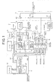
- Fig. 1 shows a video apparatus in which an embodiment of a video mixing apparatus according to the invention is applied.
- a common data bus B1 and a common address bus B2 are provided.
- a CPU 1 a ROM 2, a RAM 3, a VDC (Video Display Controller) 4, a VCE (Video Control Encoder) 5, and a data selector 6 are connected to the buses B1 and B2.
- the CPU 1 controls the whole video apparatus and outputs commands and data to the buses B1 and B2 in accordance with a program which has previously been written in the ROM 2.
- the ROM 2 is detachably provided in the video apparatus.
- VDC 4 writes data into a V-RAM (Video RAM) 12 or reads out the necessary image data from the V-RAM 12 and outputs the read-out image data in accordance with a command from the CPU 1.
- V-RAM Video RAM
- a sprite register 41, a background register 42, and a priority circuit 43 are provided in the VDC 4.
- Image data of eight bits indicative of a character video image such as a person, characters, or the like is read out from the V-RAM 12 and held in the sprite register 41 dot by dot.
- Image data of eight bits indicative of a background video image is read out from the V-RAM 12 and held in the background register 42 dot by dot.
- the priority circuit 43 selectively outputs either one of the image data held in the registers 41 and 42 in accordance with the priority indicated by a priority signal which is supplied from the CPU 1.
- the image data which is held in the sprite register 41 is the data of a screen A of a character image among the graphics video images comprising three screens.
- the image data held in the background register 42 is the data of either one of two screens B and C with respect to the background image. As shown in Table 1, all of image data VDO to VD7 of the screen C are equal to 0. The image data VDO to VD7 of the screens A and B are different as shown by reference character "X and are not all equal to O and are not constant. A most significant bit VD8 is set to "1" for the screen A of the character video image and is set to "0" for the screens B and C of the background image. The most significant bit VD8 is added at the time of output of data in each of the registers 41 and 42. The image data is, consequently, supplied from the VDC 4 to the VCE 5 and an image judging circuit 7 as 9-bit data.
- VDC 4 A specific construction of the VDC 4 is described in Japanese Patent Application Kokai No. 64-78319 (publication number JP1078319 and having patent family members GB-A-2246935 and GB-A-2210238). screen VD8 VD7 VD6 VD5 VD4 VD3 VD2 VD1 VD0 A 1 X X X X X X X X B 0 X X X X X X C 0 0 0 0 0 0 0 0 0 0 0 0 0 0 0 0 0 0 0 0 0 0 0 0 0 0 0 0 0 0 0 0 0 0 0 0 0 0 0 0 0 0 0 0 0 0 0 0 0 0 0 0 0 0 0 0 0 0 0 0 0 0 0 0 0 0 0
- the VCE 5 has a color table memory 51, an RGB-D/A converting circuit 52, and a sync signal generating circuit 53.
- the color table memory 51 is constructed by a ROM forming a color table in which RGB data of, for example, 256 colors indicative of color tones corresponding to the image data have been stored.
- the RGB data corresponding to the image data outputted from the VDC 4 is supplied from the memory 51 to the RGB-D/A converter circuit 52.
- the RGB-D/A converter circuit 52 converts the RGB data into the analog RGB signal.
- the sync signal generating circuit 53 is constructed by a frequency divider and divides a reference clock signal CLK and generates a horizontal sync signal HSYNC, a vertical sync signal VSYNC, and a dot clock signal DCLK of one pixel unit. Those signals are supplied as timing signals to the VDC 4.
- the horizontal sync signal HSYNC is supplied from the sync signal generating circuit 53 to the data selector 6 and RGB encoder 8.
- a reset signal VRESET according to the vertical sync signal is further supplied to a video signal source 10.
- the analog RGB signal outputted from the RGB-D/A converter circuit 52 is supplied to an RGB encoder 8.
- the RGB encoder 8 converts the analog RGB signal into the composite video signal in response to the horizontal sync signal HSYNC.
- the video signal after completion of the conversion is supplied as a graphics video signal to a mixing circuit 9.
- the mixing circuit 9 comprises: an attenuator 91 to attenuate the playback video signal from the video signal source 10 such as a video disk player or the like; an attenuator 92 to attenuate the graphics video signal from the encoder 8; an inverter 93 to invert the fade data which has been relayed by a change-over switch 11, which will be explained hereinbelow; and an adder 94 to add output video signals of the attenuators 91 and 92.
- the degree of attenuation of the attenuator 91 changes in accordance with the fade data supplied.
- the degree of attenuation of the attenuator 92 changes in accordance with the data inverted by the inverter 93.
- the output signals of the attenuators 91 and 92 are supplied to a CRT display (not shown) through the adder 94.
- Each of the attenuators 91 and 92 is, for example, constructed by: a VCA (Voltage Controlled Amplifier) provided in a video signal line; and a D/A converter for converting the fade data or the like into an analog signal and supplying it as a control voltage to the VCA.
- VCA Voltage Controlled Amplifier
- the data selector 6 has three registers 61 through 63 corresponding to the screens A to C and latch circuits 64 through 66 connected to the registers 61 through 63. Fade data and Address data are supplied from the CPU 1 to the registers 61 through 63 through the data bus B1 and address bus B2. The fade data is loaded into the register designated by the address data. The fade data loaded in the registers 61 through 63 is further held into the corresponding latch circuits 64 through 66 in response to the horizontal sync signal HSYNC.
- the change-over switch 11 is connected to the outputs of the latch circuits 64 through 66. The switch 11 relays and transfers the fade data held in one of the latch circuits 64 through 66 to the mixing circuit 9.
- the image judging circuit 7 discriminates to which one of the screens A, B, and C the 9-bit image data that is supplied corresponds.
- the image judging circuit 7 is constructed by an OR circuit to get the OR of the bits VDO to VD7 among the image data VDO to VD8. Two bits, the output of the OR circuit and VD8 are outputted as an output signal. This output signal is used as a control signal of the change-over switch 11.
- the CPU 1 first reads out the color data indicative of the display color and the character data of a person or the like from the ROM 2 in accordance with the program data derived from the ROM 2.
- the CPU 1 supplies the read-out color data and character data to the VDC 4 together with the address data.
- the VDC 4 allows the data to be stored at the memory location in the V-RAM 12 that is designated by the corresponding address data for every data supplied.
- the pattern number and sprite color stored in a sprite attribute table buffer are read out and the color data and character data are read out from the memory locations in the V-RAM 12 on the basis of the read-out pattern number and sprite color and loaded as image data of one dot into the sprite register 41.
- the address data is obtained from the raster position, the color data and character data in the V-RAM 12 corresponding to the address data are obtained, and further the data is derived from the address location that is decided by the character data and is loaded together with the color data into the background register 42 as image data of one dot.
- the image data VDO to VD7 held in the sprite register 41 and background register 42 are updated, for instance, every dot clock and changed at any time. Since the practical operation about the data transfer between the VDC 4 and the V-RAM 12 has been disclosed in Japanese Patent Application Kokai No. 64-78319 (publication number JP1078319 and having patent Family members GB-A-2246935 and GB-A-2210238) mentioned above, a detailed description of the operation is omitted here.
- the CPU 1 generates a priority signal every dot clock signal DCLK in accordance with the program stored in the ROM 2.
- the priority circuit 43 selectively outputs either one of the image data held in the registers 41 and 42 in accordance with the priority shown by the priority signal. Since the VD8 of one bit which has been predetermined for the screens A, B, and C is added to the image data as mentioned above when the data is outputted from each of the registers 41 and 42, the selected image data is outputted from the priority circuit 43 as nine bits of VDO to VD8.
- Fig. 2B shows the generation of a color burst signal.
- Fig. 2C shows a period of time T which is displayed on the screen of the CRT display.
- Fig. 3 shows a change in image data of every dot in the portion of the period T1 in Fig. 2.
- Fig. 3A shows the dot clock signal DCLK.
- Fig. 3B shows a period of time which is displayed on the screen of the CRT display in a manner similar to Fig. 2C.
- Fig. 3C shows a change in most significant bit VD8 of the image data that is outputted from the priority circuit 43.
- Fig. 3D shows changes in bits VDO to VD7 of the image data which is outputted from the priority circuit 43. That is, new image data VDO to VD8 are outputted every dot from the priority circuit 43.
- the image data outputted from the VDC 4 is converted into the corresponding RGB data in accordance with the color table in the color table memory 51 and is further converted into the analog RGB signal by the RGB-D/A converter circuit 52 subsequently.
- the RGB signal is supplied as a graphics video signal to the mixing circuit 9 through the RGB encoder 8.
- the screens A, B, and C are discriminated in the image judging circuit 7 in accordance with the image data outputted from the VDC 4.
- the result of the discrimination is supplied to the change-over switch 11 as a switch change-over signal.
- the switch 11 When the image data indicates the screen A, the switch 11 is switched to a selection position a.
- the switch 11 is switched to a selection position b.
- the switch 11 is switched to a selection position c.
- the CPU 1 properly supplies the fade data and address data to the data selector 6 in accordance with the program stored in the ROM 2. Therefore, the fade data is loaded into one of the registers 61 through 63 that is designated by the address data and is updated by the supplied fade data in the case where the fade data has already been loaded into the register. As shown in Figs. 4B through 4D, fade data FA through FC are ordinarily supplied to the registers 61 through 63 in one H period of time after the leading edge of the horizontal sync signal HSYNC (Fig. 4A) and the contents of the data held in those registers are changed.
- the latch circuits 64 through 66 Since the horizontal sync signal HSYNC is supplied to the latch circuits 64 through 66, the latch circuits 64 through 66 receive the fade data FA to FC held in the corresponding registers 61 through 63 in response to the leading edge of the horizontal sync signal HSYNC and update and hold them in response to the leading edge of the horizontal sync signal HSYNC as shown in Figs. 4E to 4G. Therefore, the data shown in the hatched portions in Figs. 4B through 4D is shifted as data in the hatched portions in Figs. 4E through 4G as shown by the arrows In the case where, for example, the most significant bit VD8 of the image data outputted from the VDC 4 changes every dot by the above updating operation as shown in Fig.
- the fade data is changed to either one of FA to FC as shown in Fig. 5C.
- the contents of the fade data newly held in the latch circuits 64 through 66 are not changed.
- One of the three fade data FA to FC is selected by the switch 11 and supplied to the mixing circuit 9.
- the playback video signal is supplied from the video signal source 10 to the mixing circuit 9.
- the attenuation degree of the attenuator 91 to attenuate the playback video signal is changed in accordance with the selected fade data.
- the attenuation degree of the attenuator 92 to attenuate the graphics video signal is changed by the inverter 93 in accordance with the inverted data.
- the fade data consists of four bits, so long as the fade data indicates "0000" as an opaque state, the attenuation degree of the attenuator 92 is minimum and the attenuation degree of the attenuator 91 is maximum.
- the graphics video signal is outputted as it is from the mixing circuit 9.
- the fade data indicates "1111" as a completely transparent state, the attenuation degree of the attenuator 92 is maximum and the attenuation degree of the attenuator 91 is minimum.
- the playback video signal is outputted as it is from the mixing circuit 9. The larger the transparency degree of the fade data, the higher the attenuation degree of the attenuator 92 and the lower attenuation degree of the attenuator 91.
- the output signals of the attenuators 91 and 92 are supplied to the CRT display through the adder 94.
- the video image such that the graphics image is added to the playback video image such as a moving image or the like is displayed on the screen of the CRT display.
- the degree of mixing of the playback video image and the graphics image changes, at most, every one line in the screen.
- one of the screens A, B, and C is selected every dot of the image frame with respect to the graphics image in one line of the image frame, it is possible to set so that the fade data differs every dot. In such a case, the mixing degree of the playback video image and the graphics image changes every dot.
- Fig. 6 shows another embodiment of the invention.
- a register 67 and a latch circuit 68 are provided for the data selector 6 in addition to the registers 61 through 63 and the latch circuits 64 through 66.
- the registers 61 through 63 and the latch circuits 64 through 66 are used to hold the fade data for the graphics video signal.
- the register 67 and the latch circuit 68 are used to hold the fade data for the playback video signal.
- the relayed output by the switch 11 is directly supplied to the attenuator 92.
- An output of the latch circuit 68 is directly supplied to the attenuator 91. Therefore, the inverter 93 in the apparatus of Fig. 1 is not provided for the mixing circuit 9.
- the CPU 1 properly supplies the fade data and address data to the data selector 6 in accordance with the program stored in the ROM 2.
- the fade data therefore, is held in one of the registers 61 through 63 and 67 that is designated by the address data.
- the fade data is updated by the fade data supplied.
- Each of the latch circuits 64 through 66 and 68 receives the fade data held in the corresponding one of the registers 61 through 63 and 67 and updates and holds the received fade data in response to the leading edge of the horizontal sync signal HSYNC.
- the other operations are similar to those of the apparatus shown in Fig. 1.
- the fade data supplied to the attenuator 91 and the fade data supplied to the attenuator 92 at the same point in time are in an inverted relation similarly to those in the apparatus shown in Fig. 1. Operations are previously executed so that an inverted relation is attained between the respective fade data which are supplied to the data selector 6, at the processing state of the CPU 1 according to the program stored in the ROM 2.
- Fig. 7 shows still another embodiment of the invention.
- three on/off switches 13 through 15 are connected in parallel to an output of the RGB encoder 8.
- One of the on/off switches 13 through 15 is turned on in response to the output signal of the image judging circuit 7.
- One of attenuators 921, 922, and 923 is connected to each output of the on/off switches 13 through 15.
- the fade data held in the corresponding one of the latch circuits 64 through 66 of the data selector 6 is supplied to each of the attenuators 921 through 923.
- the graphics video signal which is supplied through the switch in the on state among the on/off switches 13 through 15 is, therefore, attenuated by a corresponding one of the attenuators 921 through 923.
- the playback video signal is attenuated by the attenuator 91 in accordance with the fade data held in the latch circuit 68. Those attenuated video signals are mixed by the adder 94 and the mixed signal is outputted.
- the other constructions are similar to those shown in Fig. 6.
- the fade data indicative of a mixing ratio of at least one line of the playback video signal and the graphics video signal is sequentially generated in accordance with a predetermined order.
- the fade data is held in the holding means and is outputted from the holding means synchronously with the horizontal sync signal.
- the levels of the playback video signal and graphics video signal are individually adjusted and the adjusted signals are added. Due to this, the playback video signal and the graphics video signal are mixed at the mixture ratio set every line of one image frame.
- various effective video images can be easily formed by mixing the graphics video image of every video image such as background, person, characters, or the like and the playback video image.
Landscapes
- Engineering & Computer Science (AREA)
- Multimedia (AREA)
- Signal Processing (AREA)
- Studio Circuits (AREA)
Description
- The present invention relates to a video mixing apparatus for mixing a playback video signal obtained by playing a recording medium and a graphics video signal obtained based on a data processing.
- An apparatus has been devised for mixing a playback video signal indicative of a moving image or a still image that is obtained by playing a recording medium such as a video disk or the like and a graphics video signal indicative of a graphics video image based on graphics data which is obtained as a subcode signal. Such an apparatus is disclosed, for example, in Japanese Patent Application Kokai No. 1-256071 (which has an equivalent EP-A-0336041). In the video mixing apparatus disclosed in this document, the playback video signal and the graphics video signal are adjusted individually through a variable resistor and added together, and resistance values of such variable resistors are changed in accordance with a manual operation, so that a mixing ratio of the playback video signal and the graphics video signal are arbitrarily determined.
- In such a conventional video mixing apparatus, however, a graphics video image and a playback video image are mixed at the same mixing ratio on one whole screen. That is, the above apparatus doesn't have a construction such that a part of one image frame of a graphics video image and the other portion thereof are mixed at different mixing ratios into a playback video image or a construction such that, on the contrary, a part of one image frame of a playback video image and the other portion thereof are mixed at different mixing ratios into a graphics video image. This means that in a television game apparatus using a graphics video image, it is impossible to form various effective video images by mixing a graphics video image of every video image such as background, person, characters, or the like and a playback video image.
- US-A-5027212 describes a computer based video and graphics display system. The preamble to claim 1 is based on that document. It is, therefore, an object of the present invention to provide a video mixing apparatus which can mix a graphics video image and a playback video image at a plurality of mixing ratios in one image frame.
- According to the present invention, there is provided a video mixing apparatus for mixing a playback video signal obtained from a recording medium and a graphics video signal obtained on the basis of the result of the process of data processing means, comprising:
- fade data generating means for generating fade data indicative of a mixing ratio between at least one line of said playback video signal and said graphics video signal;
- holding means for holding the fade data generated from said fade data generating means and for outputting the fade data; and
- mixing means for individually adjusting levels of
the playback video signal and the graphics video signal
in accordance with the fade data outputted from said
holding means and for additively mixing the adjusted
signals; characterised in that:
- said graphics video signal has a plurality of screens, and said fade data generating means generates fade data indicative of a mixing ratio between said playback video signal and each of said screens of said graphics video signal in accordance with a predetermined order,
- said holding means outputs the fade data
synchronously with a horizontal sync signal (HSYNC); and
in that said apparatus further comprises:
- data generating means for generating pixel by pixel one of a plurality of image data corresponding to said plurality of screens of said graphics video signal in accordance with a priority signal representing a priority order in the reproduction of said screens, said data generating means further providing an additional data bit for each of said generated image data for indicating to which one of said graphics video signal screens the generated image data belongs;
- means for converting the image data outputted from the data generating means into the graphics video signal; and
- judging means, receiving said image data generated by said data generating means, for judging to which one of the graphics video signal screens the image data outputted from the data generating means belongs on the basis of said additional data bit and the image data,
- wherein said fade data generating means generates the fade data for each of said screens of said graphics video signal, and said holding means holds the fade data for each of said screens of said graphic video signal, and either one of the plurality of fade data held is output to said mixing means according to the result of the discrimination by said judging means or each of the plurality of fade data held is inputted to individual level adjusting means provided in said mixing means wherein said graphics video signal is supplied according to the result of the discrimination by said judging means to one of said individual level adjusting means.
-
- In the video mixing apparatus of the invention, the fade data indicative of the mixing ratio of at least one line of the playback video signal and the graphics video signal is sequentially generated in accordance with a predetermined order. The fade data is held in the holding means and is outputted from the holding means synchronously with a horizontal sync signal. In accordance with the fade data supplied from the holding means, the levels of the playback video signal and graphics video signal are individually adjusted and the adjusted signals are added together. The playback video signal and the graphics video signal are, consequently, mixed at the mixing ratio set every line of one image frame.
- Embodiments of the present invention will be described in detail hereinbelow by way of example only and with reference to the drawings.
-
- Fig. 1 is a block diagram showing an embodiment of the present invention;
- Figs. 2A through 2C are diagrams showing operation waveforms in portions of the apparatus of Fig. 1;
- Figs. 3A through 3D are diagrams showing operation waveforms in portions of the apparatus of Fig. 1;
- Figs. 4A through 4G are diagrams showing operating states in portions of the apparatus of Fig. 1;
- Figs. 5A through 5C are diagrams showing operating states in portions of the apparatus of Fig. 1;
- Fig. 6 is a block diagram showing another embodiment of the invention; and
- Fig. 7 is a block diagram showing another embodiment of the invention.
-
- Fig. 1 shows a video apparatus in which an embodiment of a video mixing apparatus according to the invention is applied. In such a video apparatus, a common data bus B1 and a common address bus B2 are provided. A
CPU 1, aROM 2, aRAM 3, a VDC (Video Display Controller) 4, a VCE (Video Control Encoder) 5, and adata selector 6 are connected to the buses B1 and B2. TheCPU 1 controls the whole video apparatus and outputs commands and data to the buses B1 and B2 in accordance with a program which has previously been written in theROM 2. TheROM 2 is detachably provided in the video apparatus. Not only one or a plurality of programs but also data such as character data, fade data, and the like which are necessary for those programs have previously been written in theROM 2. The data read out from theROM 2 or the processed data is temporarily stored into theRAM 3. TheVDC 4 writes data into a V-RAM (Video RAM) 12 or reads out the necessary image data from the V-RAM 12 and outputs the read-out image data in accordance with a command from theCPU 1. - A
sprite register 41, abackground register 42, and apriority circuit 43 are provided in theVDC 4. Image data of eight bits indicative of a character video image such as a person, characters, or the like is read out from the V-RAM 12 and held in thesprite register 41 dot by dot. Image data of eight bits indicative of a background video image is read out from the V-RAM 12 and held in thebackground register 42 dot by dot. Thepriority circuit 43 selectively outputs either one of the image data held in theregisters CPU 1. The image data which is held in thesprite register 41 is the data of a screen A of a character image among the graphics video images comprising three screens. The image data held in thebackground register 42 is the data of either one of two screens B and C with respect to the background image. As shown in Table 1, all of image data VDO to VD7 of the screen C are equal to 0. The image data VDO to VD7 of the screens A and B are different as shown by reference character "X and are not all equal to O and are not constant. A most significant bit VD8 is set to "1" for the screen A of the character video image and is set to "0" for the screens B and C of the background image. The most significant bit VD8 is added at the time of output of data in each of theregisters VDC 4 to theVCE 5 and animage judging circuit 7 as 9-bit data. A specific construction of theVDC 4 is described in Japanese Patent Application Kokai No. 64-78319 (publication number JP1078319 and having patent family members GB-A-2246935 and GB-A-2210238).screen VD8 VD7 VD6 VD5 VD4 VD3 VD2 VD1 VD0 A 1 X X X X X X X X B 0 X X X X X X X X C 0 0 0 0 0 0 0 0 0 - The VCE 5 has a
color table memory 51, an RGB-D/A converting circuit 52, and a syncsignal generating circuit 53. Thecolor table memory 51 is constructed by a ROM forming a color table in which RGB data of, for example, 256 colors indicative of color tones corresponding to the image data have been stored. The RGB data corresponding to the image data outputted from theVDC 4 is supplied from thememory 51 to the RGB-D/A converter circuit 52. The RGB-D/A converter circuit 52 converts the RGB data into the analog RGB signal. The syncsignal generating circuit 53 is constructed by a frequency divider and divides a reference clock signal CLK and generates a horizontal sync signal HSYNC, a vertical sync signal VSYNC, and a dot clock signal DCLK of one pixel unit. Those signals are supplied as timing signals to theVDC 4. The horizontal sync signal HSYNC is supplied from the syncsignal generating circuit 53 to thedata selector 6 andRGB encoder 8. A reset signal VRESET according to the vertical sync signal is further supplied to avideo signal source 10. - The analog RGB signal outputted from the RGB-D/A
converter circuit 52 is supplied to anRGB encoder 8. TheRGB encoder 8 converts the analog RGB signal into the composite video signal in response to the horizontal sync signal HSYNC. The video signal after completion of the conversion is supplied as a graphics video signal to amixing circuit 9. The mixingcircuit 9 comprises: anattenuator 91 to attenuate the playback video signal from thevideo signal source 10 such as a video disk player or the like; anattenuator 92 to attenuate the graphics video signal from theencoder 8; aninverter 93 to invert the fade data which has been relayed by a change-over switch 11, which will be explained hereinbelow; and anadder 94 to add output video signals of theattenuators attenuator 91 changes in accordance with the fade data supplied. The degree of attenuation of theattenuator 92 changes in accordance with the data inverted by theinverter 93. The output signals of theattenuators adder 94. Each of theattenuators - The
data selector 6 has threeregisters 61 through 63 corresponding to the screens A to C and latchcircuits 64 through 66 connected to theregisters 61 through 63. Fade data and Address data are supplied from theCPU 1 to theregisters 61 through 63 through the data bus B1 and address bus B2. The fade data is loaded into the register designated by the address data. The fade data loaded in theregisters 61 through 63 is further held into thecorresponding latch circuits 64 through 66 in response to the horizontal sync signal HSYNC. The change-over switch 11 is connected to the outputs of thelatch circuits 64 through 66. Theswitch 11 relays and transfers the fade data held in one of thelatch circuits 64 through 66 to themixing circuit 9. - The
image judging circuit 7 discriminates to which one of the screens A, B, and C the 9-bit image data that is supplied corresponds. For example, theimage judging circuit 7 is constructed by an OR circuit to get the OR of the bits VDO to VD7 among the image data VDO to VD8. Two bits, the output of the OR circuit and VD8 are outputted as an output signal. This output signal is used as a control signal of the change-over switch 11. - In such a construction, the
CPU 1 first reads out the color data indicative of the display color and the character data of a person or the like from theROM 2 in accordance with the program data derived from theROM 2. TheCPU 1 supplies the read-out color data and character data to theVDC 4 together with the address data. TheVDC 4 allows the data to be stored at the memory location in the V-RAM 12 that is designated by the corresponding address data for every data supplied. - In the
VDC 4, the pattern number and sprite color stored in a sprite attribute table buffer (not shown) are read out and the color data and character data are read out from the memory locations in the V-RAM 12 on the basis of the read-out pattern number and sprite color and loaded as image data of one dot into thesprite register 41. The address data is obtained from the raster position, the color data and character data in the V-RAM 12 corresponding to the address data are obtained, and further the data is derived from the address location that is decided by the character data and is loaded together with the color data into thebackground register 42 as image data of one dot. The image data VDO to VD7 held in thesprite register 41 and background register 42 are updated, for instance, every dot clock and changed at any time. Since the practical operation about the data transfer between theVDC 4 and the V-RAM 12 has been disclosed in Japanese Patent Application Kokai No. 64-78319 (publication number JP1078319 and having patent Family members GB-A-2246935 and GB-A-2210238) mentioned above, a detailed description of the operation is omitted here. - The
CPU 1 generates a priority signal every dot clock signal DCLK in accordance with the program stored in theROM 2. Thepriority circuit 43 selectively outputs either one of the image data held in theregisters registers priority circuit 43 as nine bits of VDO to VD8. - In the case where the horizontal sync signal HSYNC is generated as shown in Fig. 2A, Fig. 2B shows the generation of a color burst signal. Fig. 2C shows a period of time T which is displayed on the screen of the CRT display. Fig. 3 shows a change in image data of every dot in the portion of the period T1 in Fig. 2. Specifically speaking, Fig. 3A shows the dot clock signal DCLK. Fig. 3B shows a period of time which is displayed on the screen of the CRT display in a manner similar to Fig. 2C. Fig. 3C shows a change in most significant bit VD8 of the image data that is outputted from the
priority circuit 43. Fig. 3D shows changes in bits VDO to VD7 of the image data which is outputted from thepriority circuit 43. That is, new image data VDO to VD8 are outputted every dot from thepriority circuit 43. - The image data outputted from the
VDC 4 is converted into the corresponding RGB data in accordance with the color table in thecolor table memory 51 and is further converted into the analog RGB signal by the RGB-D/Aconverter circuit 52 subsequently. The RGB signal is supplied as a graphics video signal to themixing circuit 9 through theRGB encoder 8. The screens A, B, and C are discriminated in theimage judging circuit 7 in accordance with the image data outputted from theVDC 4. The result of the discrimination is supplied to the change-over switch 11 as a switch change-over signal. When the image data indicates the screen A, theswitch 11 is switched to a selection position a. When the image data indicates the screen B, theswitch 11 is switched to a selection position b. When the image data indicates the screen C, theswitch 11 is switched to a selection position c. - On the other hand, the
CPU 1 properly supplies the fade data and address data to thedata selector 6 in accordance with the program stored in theROM 2. Therefore, the fade data is loaded into one of theregisters 61 through 63 that is designated by the address data and is updated by the supplied fade data in the case where the fade data has already been loaded into the register. As shown in Figs. 4B through 4D, fade data FA through FC are ordinarily supplied to theregisters 61 through 63 in one H period of time after the leading edge of the horizontal sync signal HSYNC (Fig. 4A) and the contents of the data held in those registers are changed. Since the horizontal sync signal HSYNC is supplied to thelatch circuits 64 through 66, thelatch circuits 64 through 66 receive the fade data FA to FC held in thecorresponding registers 61 through 63 in response to the leading edge of the horizontal sync signal HSYNC and update and hold them in response to the leading edge of the horizontal sync signal HSYNC as shown in Figs. 4E to 4G. Therefore, the data shown in the hatched portions in Figs. 4B through 4D is shifted as data in the hatched portions in Figs. 4E through 4G as shown by the arrows In the case where, for example, the most significant bit VD8 of the image data outputted from theVDC 4 changes every dot by the above updating operation as shown in Fig. 5A, or, in the case where the OR outputs of the bits VDO to VD7 are changed every dot as shown in Fig. 5B, the fade data is changed to either one of FA to FC as shown in Fig. 5C. When there is no change in fade data held in thecorresponding registers 61 through 63, the contents of the fade data newly held in thelatch circuits 64 through 66 are not changed. - One of the three fade data FA to FC is selected by the
switch 11 and supplied to themixing circuit 9. In addition to the graphics video signal and one of the fade data FA to FC, the playback video signal is supplied from thevideo signal source 10 to themixing circuit 9. In themixing circuit 9, the attenuation degree of theattenuator 91 to attenuate the playback video signal is changed in accordance with the selected fade data. The attenuation degree of theattenuator 92 to attenuate the graphics video signal is changed by theinverter 93 in accordance with the inverted data. Now, assuming that the fade data consists of four bits, so long as the fade data indicates "0000" as an opaque state, the attenuation degree of theattenuator 92 is minimum and the attenuation degree of theattenuator 91 is maximum. The graphics video signal is outputted as it is from the mixingcircuit 9. When the fade data indicates "1111" as a completely transparent state, the attenuation degree of theattenuator 92 is maximum and the attenuation degree of theattenuator 91 is minimum. The playback video signal is outputted as it is from the mixingcircuit 9. The larger the transparency degree of the fade data, the higher the attenuation degree of theattenuator 92 and the lower attenuation degree of theattenuator 91. The larger the transparency degree, the higher the overlap degree of the playback video image to the graphics image. The output signals of theattenuators adder 94. For example, the video image such that the graphics image is added to the playback video image such as a moving image or the like is displayed on the screen of the CRT display. In such a video image, the degree of mixing of the playback video image and the graphics image changes, at most, every one line in the screen. Further, since one of the screens A, B, and C is selected every dot of the image frame with respect to the graphics image in one line of the image frame, it is possible to set so that the fade data differs every dot. In such a case, the mixing degree of the playback video image and the graphics image changes every dot. - Fig. 6 shows another embodiment of the invention. In this video mixing apparatus, a
register 67 and alatch circuit 68 are provided for thedata selector 6 in addition to theregisters 61 through 63 and thelatch circuits 64 through 66. Theregisters 61 through 63 and thelatch circuits 64 through 66 are used to hold the fade data for the graphics video signal. Theregister 67 and thelatch circuit 68 are used to hold the fade data for the playback video signal. The relayed output by theswitch 11 is directly supplied to theattenuator 92. An output of thelatch circuit 68 is directly supplied to theattenuator 91. Therefore, theinverter 93 in the apparatus of Fig. 1 is not provided for themixing circuit 9. TheCPU 1 properly supplies the fade data and address data to thedata selector 6 in accordance with the program stored in theROM 2. The fade data, therefore, is held in one of theregisters 61 through 63 and 67 that is designated by the address data. When the fade data has already been loaded into such a register, it is updated by the fade data supplied. Each of thelatch circuits 64 through 66 and 68 receives the fade data held in the corresponding one of theregisters 61 through 63 and 67 and updates and holds the received fade data in response to the leading edge of the horizontal sync signal HSYNC. The other operations are similar to those of the apparatus shown in Fig. 1. The fade data supplied to theattenuator 91 and the fade data supplied to theattenuator 92 at the same point in time are in an inverted relation similarly to those in the apparatus shown in Fig. 1. Operations are previously executed so that an inverted relation is attained between the respective fade data which are supplied to thedata selector 6, at the processing state of theCPU 1 according to the program stored in theROM 2. - Fig. 7 shows still another embodiment of the invention. In this embodiment, three on/off switches 13 through 15 are connected in parallel to an output of the
RGB encoder 8. One of the on/off switches 13 through 15 is turned on in response to the output signal of theimage judging circuit 7. One ofattenuators latch circuits 64 through 66 of thedata selector 6 is supplied to each of theattenuators 921 through 923. The graphics video signal which is supplied through the switch in the on state among the on/off switches 13 through 15 is, therefore, attenuated by a corresponding one of theattenuators 921 through 923. The playback video signal is attenuated by theattenuator 91 in accordance with the fade data held in thelatch circuit 68. Those attenuated video signals are mixed by theadder 94 and the mixed signal is outputted. The other constructions are similar to those shown in Fig. 6. - According to the video mixing apparatus of the present invention as mentioned above, the fade data indicative of a mixing ratio of at least one line of the playback video signal and the graphics video signal is sequentially generated in accordance with a predetermined order. The fade data is held in the holding means and is outputted from the holding means synchronously with the horizontal sync signal. In accordance with the fade data outputted from the holding means, the levels of the playback video signal and graphics video signal are individually adjusted and the adjusted signals are added. Due to this, the playback video signal and the graphics video signal are mixed at the mixture ratio set every line of one image frame. In the video apparatus using the graphics video image, accordingly, various effective video images can be easily formed by mixing the graphics video image of every video image such as background, person, characters, or the like and the playback video image.
Claims (2)
- A video mixing apparatus for mixing a playback video signal obtained from a recording medium (10) and a graphics video signal obtained on the basis of the result of the process of data processing means (1,4,12), comprising:fade data generating means (1,6) for generating fade data indicative of a mixing ratio between at least one line of said playback video signal and said graphics video signal;holding means (64,65,66,68) for holding the fade data generated from said fade data generating means and for outputting the fade data; andmixing means (91,92,93,94) for individually adjusting levels of the playback video signal and the graphics video signal in accordance with the fade data outputted from said holding means and for additively mixing the adjusted signals; characterised in that:said graphics video signal has a plurality of screens, and said fade data generating means generates fade data indicative of a mixing ratio between said playback video signal and each of said screens of said graphics video signal in accordance with a predetermined order,said holding means outputs the fade data synchronously with a horizontal sync signal (HSYNC); and in that said apparatus further comprises:data generating means (4,12) for generating pixel by pixel one of a plurality of image data corresponding to said plurality of screens of said graphics video signal in accordance with a priority signal representing a priority order in the reproduction of said screens, said data generating means further providing an additional data bit for each of said generated image data for indicating to which one of said graphics video signal screens the generated image data belongs;means (5) for converting the image data outputted from the data generating means into the graphics video signal; andjudging means (7), receiving said image data generated by said data generating means, for judging to which one of the graphics video signal screens the image data outputted from the data generating means belongs on the basis of said additional data bit and the image data,wherein said fade data generating means generates the fade data for each of said screens of said graphics video signal, and said holding means holds the fade data for each of said screens of said graphic video signal, and either one of the plurality of fade data held is output to said mixing means, according to the result of the discrimination by said judging means or each of the plurality of fade data held is inputted to individual level adjusting means (921, 922, 923) provided in said mixing means wherein said graphics video signal is supplied according to the result of the discrimination by said judging means to one of said individual level adjusting means.
- The video mixing apparatus of claim 1, wherein said judging means discriminates said one screen by evaluating the bit arrangement of said image data.
Applications Claiming Priority (3)
| Application Number | Priority Date | Filing Date | Title |
|---|---|---|---|
| JP14303992 | 1992-06-03 | ||
| JP4143039A JP3059302B2 (en) | 1992-06-03 | 1992-06-03 | Video mixing device |
| JP143039/92 | 1992-06-03 |
Publications (2)
| Publication Number | Publication Date |
|---|---|
| EP0573293A1 EP0573293A1 (en) | 1993-12-08 |
| EP0573293B1 true EP0573293B1 (en) | 2001-09-05 |
Family
ID=15329488
Family Applications (1)
| Application Number | Title | Priority Date | Filing Date |
|---|---|---|---|
| EP93304314A Expired - Lifetime EP0573293B1 (en) | 1992-06-03 | 1993-06-03 | Video mixing apparatus |
Country Status (4)
| Country | Link |
|---|---|
| US (1) | US5355175A (en) |
| EP (1) | EP0573293B1 (en) |
| JP (1) | JP3059302B2 (en) |
| DE (1) | DE69330692T2 (en) |
Families Citing this family (10)
| Publication number | Priority date | Publication date | Assignee | Title |
|---|---|---|---|---|
| US5471570A (en) * | 1993-12-30 | 1995-11-28 | International Business Machines Corporation | Hardware XOR sprite for computer display systems |
| US5502504A (en) † | 1994-04-28 | 1996-03-26 | Prevue Networks, Inc. | Video mix program guide |
| ES2143092T4 (en) * | 1994-12-14 | 2011-11-22 | Koninklijke Philips Electronics N.V. | SUBTITLE TRANSMISSION SYSTEM. |
| US5880739A (en) * | 1995-06-06 | 1999-03-09 | Compaq Computer Corporation | Blitting of images using instructions |
| US5739868A (en) * | 1995-08-31 | 1998-04-14 | General Instrument Corporation Of Delaware | Apparatus for processing mixed YUV and color palettized video signals |
| US5835103A (en) | 1995-08-31 | 1998-11-10 | General Instrument Corporation | Apparatus using memory control tables related to video graphics processing for TV receivers |
| US5838296A (en) | 1995-08-31 | 1998-11-17 | General Instrument Corporation | Apparatus for changing the magnification of video graphics prior to display therefor on a TV screen |
| US6023302A (en) * | 1996-03-07 | 2000-02-08 | Powertv, Inc. | Blending of video images in a home communications terminal |
| JPH10322651A (en) * | 1997-05-19 | 1998-12-04 | Sony Corp | Reproducing device, recorder and recording medium |
| US6573946B1 (en) * | 2000-08-31 | 2003-06-03 | Intel Corporation | Synchronizing video streams with different pixel clock rates |
Family Cites Families (7)
| Publication number | Priority date | Publication date | Assignee | Title |
|---|---|---|---|---|
| US4680622A (en) * | 1985-02-11 | 1987-07-14 | Ncr Corporation | Apparatus and method for mixing video signals for simultaneous presentation |
| CA1310771C (en) * | 1987-05-18 | 1992-11-24 | Ivan J. Maltz | Video compositing using a software linear keyer |
| JPH07118798B2 (en) * | 1988-02-29 | 1995-12-18 | パイオニア株式会社 | Image information recording and reproducing method |
| DE3842977C2 (en) * | 1988-12-21 | 1996-03-28 | Broadcast Television Syst | Mixing device for video signals |
| DE69030549T2 (en) * | 1989-10-16 | 1997-09-04 | Sony Corp | Device for digital video fading |
| US5220433A (en) * | 1989-10-31 | 1993-06-15 | Asahi Kogaku Kogyo Kabushiki Kaisha | Still video apparatus including picture and sound fading |
| US5027212A (en) * | 1989-12-06 | 1991-06-25 | Videologic Limited | Computer based video/graphics display system |
-
1992
- 1992-06-03 JP JP4143039A patent/JP3059302B2/en not_active Expired - Fee Related
-
1993
- 1993-06-02 US US08/071,014 patent/US5355175A/en not_active Expired - Fee Related
- 1993-06-03 DE DE69330692T patent/DE69330692T2/en not_active Expired - Fee Related
- 1993-06-03 EP EP93304314A patent/EP0573293B1/en not_active Expired - Lifetime
Also Published As
| Publication number | Publication date |
|---|---|
| DE69330692D1 (en) | 2001-10-11 |
| US5355175A (en) | 1994-10-11 |
| EP0573293A1 (en) | 1993-12-08 |
| JP3059302B2 (en) | 2000-07-04 |
| DE69330692T2 (en) | 2002-06-20 |
| JPH05336440A (en) | 1993-12-17 |
Similar Documents
| Publication | Publication Date | Title |
|---|---|---|
| US4980678A (en) | Display controller for CRT/flat panel display apparatus | |
| US5467442A (en) | Image processing apparatus | |
| US4951038A (en) | Apparatus for displaying a sprite on a screen | |
| US5579028A (en) | Apparatus for mixing play video signal with graphics video signal | |
| EP0573293B1 (en) | Video mixing apparatus | |
| EP0366871B1 (en) | Apparatus for processing video signal | |
| JPS6360395B2 (en) | ||
| US4804948A (en) | Video display control system | |
| US5140312A (en) | Display apparatus | |
| US5319786A (en) | Apparatus for controlling a scanning type video display to be divided into plural display regions | |
| US4931785A (en) | Display apparatus | |
| JPH10145806A (en) | White balance adjustment circuit | |
| KR960014826B1 (en) | An apparatus for controlling the access of a video memory | |
| JPH06180569A (en) | Image processor | |
| US5781183A (en) | Image processing apparatus including selecting function for displayed colors | |
| JPH0683295A (en) | Multimedia display system | |
| EP0159851B1 (en) | Advanced video processor with hardware scrolling | |
| JP2780663B2 (en) | Image display method and device for personal computer education support system | |
| JP2582743B2 (en) | Image processing device | |
| JPH0413894Y2 (en) | ||
| RU1836719C (en) | Device for displaying of graphic information on colour tv indicator | |
| JPH07261730A (en) | Picture display device and television game machine using same | |
| JPH087555B2 (en) | Display synthesizer | |
| JPH06295171A (en) | Image processor | |
| JPH07274086A (en) | Display controller |
Legal Events
| Date | Code | Title | Description |
|---|---|---|---|
| PUAI | Public reference made under article 153(3) epc to a published international application that has entered the european phase |
Free format text: ORIGINAL CODE: 0009012 |
|
| AK | Designated contracting states |
Kind code of ref document: A1 Designated state(s): DE FR GB |
|
| 17P | Request for examination filed |
Effective date: 19940108 |
|
| RIN1 | Information on inventor provided before grant (corrected) |
Inventor name: MIYAZAKI, MASAKAZU, C/O PIONEER TOKOROZAWA PLANT Inventor name: MATSUURA, HIROYASU, C/O PIONEER TOKOROZAWA PLANT Inventor name: YAMAZAKI, HITOSHI, C/O PIONEER TOKOROZAWA PLANT Inventor name: YOSHIMI, TAKASHI, C/O PIONEER TOKOROZAWA PLANT Inventor name: NAGASE, YOSHINOU, C/O PIONEER TOKOROZAWA PLANT Inventor name: OKAMOTO, MANABU, C/O PIONEER TOKOROZAWA PLANT Inventor name: TAKEYA, NORIYOSHI, C/O PIONEER TOKOROZAWA PLANT Inventor name: OKADA, SETSUO |
|
| 17Q | First examination report despatched |
Effective date: 19940727 |
|
| GRAG | Despatch of communication of intention to grant |
Free format text: ORIGINAL CODE: EPIDOS AGRA |
|
| GRAG | Despatch of communication of intention to grant |
Free format text: ORIGINAL CODE: EPIDOS AGRA |
|
| GRAH | Despatch of communication of intention to grant a patent |
Free format text: ORIGINAL CODE: EPIDOS IGRA |
|
| GRAH | Despatch of communication of intention to grant a patent |
Free format text: ORIGINAL CODE: EPIDOS IGRA |
|
| GRAA | (expected) grant |
Free format text: ORIGINAL CODE: 0009210 |
|
| AK | Designated contracting states |
Kind code of ref document: B1 Designated state(s): DE FR GB |
|
| REF | Corresponds to: |
Ref document number: 69330692 Country of ref document: DE Date of ref document: 20011011 |
|
| ET | Fr: translation filed | ||
| REG | Reference to a national code |
Ref country code: GB Ref legal event code: IF02 |
|
| REG | Reference to a national code |
Ref country code: GB Ref legal event code: 746 Effective date: 20020411 |
|
| PLBE | No opposition filed within time limit |
Free format text: ORIGINAL CODE: 0009261 |
|
| STAA | Information on the status of an ep patent application or granted ep patent |
Free format text: STATUS: NO OPPOSITION FILED WITHIN TIME LIMIT |
|
| REG | Reference to a national code |
Ref country code: FR Ref legal event code: D6 |
|
| 26N | No opposition filed | ||
| PGFP | Annual fee paid to national office [announced via postgrant information from national office to epo] |
Ref country code: GB Payment date: 20040602 Year of fee payment: 12 |
|
| PGFP | Annual fee paid to national office [announced via postgrant information from national office to epo] |
Ref country code: FR Payment date: 20040608 Year of fee payment: 12 |
|
| PGFP | Annual fee paid to national office [announced via postgrant information from national office to epo] |
Ref country code: DE Payment date: 20040610 Year of fee payment: 12 |
|
| PG25 | Lapsed in a contracting state [announced via postgrant information from national office to epo] |
Ref country code: GB Free format text: LAPSE BECAUSE OF NON-PAYMENT OF DUE FEES Effective date: 20050603 |
|
| PG25 | Lapsed in a contracting state [announced via postgrant information from national office to epo] |
Ref country code: DE Free format text: LAPSE BECAUSE OF NON-PAYMENT OF DUE FEES Effective date: 20060103 |
|
| PG25 | Lapsed in a contracting state [announced via postgrant information from national office to epo] |
Ref country code: FR Free format text: LAPSE BECAUSE OF NON-PAYMENT OF DUE FEES Effective date: 20060228 |
|
| GBPC | Gb: european patent ceased through non-payment of renewal fee |
Effective date: 20050603 |
|
| REG | Reference to a national code |
Ref country code: FR Ref legal event code: ST Effective date: 20060228 |