EP0570883A2 - A magnetoresistive head - Google Patents
A magnetoresistive head Download PDFInfo
- Publication number
- EP0570883A2 EP0570883A2 EP93108005A EP93108005A EP0570883A2 EP 0570883 A2 EP0570883 A2 EP 0570883A2 EP 93108005 A EP93108005 A EP 93108005A EP 93108005 A EP93108005 A EP 93108005A EP 0570883 A2 EP0570883 A2 EP 0570883A2
- Authority
- EP
- European Patent Office
- Prior art keywords
- layer
- ferromagnetic
- magnetoresistive effect
- bias
- magnetic field
- Prior art date
- Legal status (The legal status is an assumption and is not a legal conclusion. Google has not performed a legal analysis and makes no representation as to the accuracy of the status listed.)
- Granted
Links
Images


Classifications
-
- G—PHYSICS
- G11—INFORMATION STORAGE
- G11B—INFORMATION STORAGE BASED ON RELATIVE MOVEMENT BETWEEN RECORD CARRIER AND TRANSDUCER
- G11B5/00—Recording by magnetisation or demagnetisation of a record carrier; Reproducing by magnetic means; Record carriers therefor
- G11B5/127—Structure or manufacture of heads, e.g. inductive
- G11B5/33—Structure or manufacture of flux-sensitive heads, i.e. for reproduction only; Combination of such heads with means for recording or erasing only
- G11B5/39—Structure or manufacture of flux-sensitive heads, i.e. for reproduction only; Combination of such heads with means for recording or erasing only using magneto-resistive devices or effects
- G11B5/3903—Structure or manufacture of flux-sensitive heads, i.e. for reproduction only; Combination of such heads with means for recording or erasing only using magneto-resistive devices or effects using magnetic thin film layers or their effects, the films being part of integrated structures
- G11B5/3906—Details related to the use of magnetic thin film layers or to their effects
- G11B5/3929—Disposition of magnetic thin films not used for directly coupling magnetic flux from the track to the MR film or for shielding
- G11B5/3932—Magnetic biasing films
-
- Y—GENERAL TAGGING OF NEW TECHNOLOGICAL DEVELOPMENTS; GENERAL TAGGING OF CROSS-SECTIONAL TECHNOLOGIES SPANNING OVER SEVERAL SECTIONS OF THE IPC; TECHNICAL SUBJECTS COVERED BY FORMER USPC CROSS-REFERENCE ART COLLECTIONS [XRACs] AND DIGESTS
- Y10—TECHNICAL SUBJECTS COVERED BY FORMER USPC
- Y10S—TECHNICAL SUBJECTS COVERED BY FORMER USPC CROSS-REFERENCE ART COLLECTIONS [XRACs] AND DIGESTS
- Y10S428/00—Stock material or miscellaneous articles
- Y10S428/90—Magnetic feature
-
- Y—GENERAL TAGGING OF NEW TECHNOLOGICAL DEVELOPMENTS; GENERAL TAGGING OF CROSS-SECTIONAL TECHNOLOGIES SPANNING OVER SEVERAL SECTIONS OF THE IPC; TECHNICAL SUBJECTS COVERED BY FORMER USPC CROSS-REFERENCE ART COLLECTIONS [XRACs] AND DIGESTS
- Y10—TECHNICAL SUBJECTS COVERED BY FORMER USPC
- Y10T—TECHNICAL SUBJECTS COVERED BY FORMER US CLASSIFICATION
- Y10T428/00—Stock material or miscellaneous articles
- Y10T428/11—Magnetic recording head
- Y10T428/1171—Magnetic recording head with defined laminate structural detail
-
- Y—GENERAL TAGGING OF NEW TECHNOLOGICAL DEVELOPMENTS; GENERAL TAGGING OF CROSS-SECTIONAL TECHNOLOGIES SPANNING OVER SEVERAL SECTIONS OF THE IPC; TECHNICAL SUBJECTS COVERED BY FORMER USPC CROSS-REFERENCE ART COLLECTIONS [XRACs] AND DIGESTS
- Y10—TECHNICAL SUBJECTS COVERED BY FORMER USPC
- Y10T—TECHNICAL SUBJECTS COVERED BY FORMER US CLASSIFICATION
- Y10T428/00—Stock material or miscellaneous articles
- Y10T428/12—All metal or with adjacent metals
- Y10T428/12493—Composite; i.e., plural, adjacent, spatially distinct metal components [e.g., layers, joint, etc.]
- Y10T428/12771—Transition metal-base component
- Y10T428/12861—Group VIII or IB metal-base component
- Y10T428/12931—Co-, Fe-, or Ni-base components, alternative to each other
Definitions
- the present invention relates to a magnetoresistive head (hereinafter referred to as an MR head), which comprises a ferromagnetic magnetoresistive effect element (hereinafter referred to as an MR element) making use of a ferromagnetic magnetoresistive effect for reproducing magnetic information written in a magnetic recording medium.
- an MR head which comprises a ferromagnetic magnetoresistive effect element (hereinafter referred to as an MR element) making use of a ferromagnetic magnetoresistive effect for reproducing magnetic information written in a magnetic recording medium.
- the MR element is capable of producing a high level output independent of the relative velocity of the element and recording medium, and its application to a reproducing head of small size and high density magnetic recording apparatus has been in focus.
- the MR element it is necessary to meet two basic requirements.
- a first requirement is that the MR element is capable of linear response to the magnetic information written in the magnetic recording medium.
- a bias magnetic field is applied in a direction orthogonal to a sense current flowing in the MR element (hereinafter referred to as transversal bias magnetic field) so as to set the angle ⁇ between the sense current and the magnetization M of the MR element (hereinafter referred to as bias angle) to a predetermined value (desirably 45 degrees).
- bias angle a predetermined value (desirably 45 degrees).
- United States Patent No. 3,864,751 discloses a structure, in which a soft magnetic bias-assistant layer or a soft adjacent layer and an MR element are laminated with an intervening electric insulating layer.
- This United States Patent also discloses a method, in which a soft bias-assistant layer is magnetized by supplying a sense current to the MR element, while using a magnetic field generated by the soft magnetic bias-assistant layer to apply the transversal bias magnetic field to the MR element.
- Japanese Utility Model Laid-Open No. 159,518/1985 discloses a structure, in which a non-crystalline soft magnetic bias-assistant layer and an MR element are laminated with an intervening non-magnetic conductive layer. In this structure, the resistivity of the non-crystalline soft magnetic bias-assistant layer is extremely high compared to the resistivity of the MR element.
- the second requirement is to suppress Barkhausen noise, which is a main cause of reproduced signal noise and deteriorates the quality of the reproduced signal.
- the Barkhausen noise is thought to stem from the movement of magnetic walls generated by an inverse magnetic field at an end of the MR element. Accordingly, there have been proposed a number of methods of eliminating the magnetic walls by making the MR element part to be of a single domain.
- Japanese Patent Laid-Open No. 40,610/1987 discloses a structure, in which an anti-ferromagnetic material is provided at each MR element end to make use of mutual exchange action of the two portions of the anti-ferromagnetic material for applying a bias magnetic field in the sense current direction (hereinafter referred to as longitudinal bias magnetic field).
- a first restriction is that it is necessary to form the anti-ferromagnetic layer in direct contact with the ferromagnetic magnetoresistive effect layer since the bias magnetic field is generated with the exchange force.
- a second restriction is that the anti-ferromagnetic material has to be patterned such as to be present only at opposite end portions of the MR element. This is so because if the exchange force is active over the entire MR element, the response character thereof is deteriorated due to a high anisotropic magnetic field in the inverse magnetic layer.
- the ferromagnetic magnetoresistive effect layer 4 and anti-ferromagnetic layer 3 are formed continuously in vacuum, and then only the anti-ferromagnetic layer 3 is etched. In this patterning, however, it is difficult to selectively etch only the anti-ferromagnetic layer 3. In addition, an over-etching will result in deterioration of the characteristic of the ferromagnetic layer.
- designated at 1 is a non-magnetic substrate, at 5 a non-magnetic conductive layer, at 6 electrodes, and at 7 a bias-assistant layer.
- Japanese Patent Application No. 124,024/1992 discloses a structure, in which a ground layer is provided only on a portion of an anti-ferromagnetic layer mainly composed of FeMn as shown in Fig. 4.
- Fig. 4 designated at 11 is a non-magnetic substrate, at 12 a soft magnetic bias-assistant layer, at 13 a ground layer, at 14 an anti-ferromagnetic layer, at 15 a ferromagnetic magnetoresistive effect layer, at 16 electrodes, and at 17 a non-magnetic conductive layer.
- the anti-ferromagnetic layer 14, which is mainly composed of FeMn has its magnetic characteristics dependent on its crystal structure.
- ⁇ phase is an inverse ferromagnetic phase which is stable at room temperature and above, it grows stably only on the ground layer 13 having the same face-centered cubic structure.
- the same effect as obtainable by patterning the anti-ferromagnetic layer 14 can be obtained by providing the ground layer 13 having a face-centered cubic structure only on a desired portion for the bias magnetic field generation with the exchange force.
- An object of the invention is therefore to provide a magnetoresistive head, which is subject to less Barkhausen noise and is simple in structure.
- a magnetoresistive head comprising a ferromagnetic magnetoresistive effect layer, an anti-ferromagnetic layer for generating a longitudinal bias magnetic field with an exchange force with respect to the ferromagnetic magnetoresistive effect layer, the anti-ferromagnetic layer being provided in direct contact with the ferromagnetic magnetoresistive effect layer and composed of or mainly composed of FeMn, and means for generating a transversal bias magnetic field in the ferromagnetic magnetoresistive effect layer, wherein a ground layer having a face-centered cubic structure is provided on only a portion of said anti-ferromagnetic layer.
- a magnetoresistive head comprising a ferromagnetic magnetoresistive effect layer, an anti-ferromagnetic layer for generating a longitudinal bias magnetic field by an exchange force with respect to the ferromagnetic magnetoresistive effect layer, and a soft magnetic bias-assistant layer for a transversal bias magnetic field in the ferromagnetic magnetoresistive effect layer, wherein the soft magnetic bias-assistant layer has a crystal structure other than a face-centered cubic structure, a ground layer having a face-centered cubic structure is provided on only a portion of the anti-ferromagnetic layer, and the soft bias-assistant layer, the ground layer, the anti-ferromagnetic layer and the ferromagnetic magnetoresistive effect layer are laminated in the mentioned order.
- Fig. 1 is a sectional view showing an example of the MR head according to the present invention.
- a ground layer 2 having a face-centered cubic structure, and it is patterned to a predetermined shape.
- an anti-ferromagnetic layer 3 On this layer, an anti-ferromagnetic layer 3, a ferromagnetic magnetoresistive effect layer 4, a non-magnetic intermediate layer 5 and a bias-assistant layer 6 are laminated in the mentioned order.
- These laminated layers are patterned to predetermined shapes, and then electrodes 7 are formed to the laminate to complete the MR head.
- the material of the substrate 1 which is a non-magnetic substrate may be used glass, Al2O3, TiC, SiC, sintering composed of Al2O3 and TiC, ferrite, etc.
- the ground layer 2 may be used Cu or alloys of NiCr or the like having face-centered cubic structures with or without additives.
- the inverse ferromagnetic layer 3 may be used anti-ferromagnetic alloys of FeMn, FeMnCr, etc. with or without additives.
- the ferromagnetic magnetoresistive effect layer 4 may be used Co, Ni or ferromagnetic alloys, e.g., Ni-Fe, Co-Fe, Co-Ni, etc., with or without additives.
- non-magnetic intermediate layer 5 may be used non-magnetic conductive alloys, e.g., Ti, Mo., Cr, Ta, etc.
- bias-assistant layer 6 may be used non-crystalline soft magnetic materials, e.g., CoZr, CoZrNb, CoZrMo, CoZrTa, CoTa, etc.
- the anti-ferromagnetic material for generating the longitudinal bias magnetic field and mainly composed of FeMn has magnetic characteristics dependent on its crystal structure, and the ⁇ phase having a face-centered cubic structure has stable anti-ferromagnetic phase at room temperature or above as stated before.
- This ⁇ phase is comparatively unstable and can steadily grow only on a ground layer having the same face-centered cubic structure.
- the same effect as that of patterning the anti-ferromagnetic layer is obtainable by providing a ground layer having a face-centered cubic structure on only a portion, in which it is desired to generate a bias magnetic field by an exchange coupling force.
- a NiCr layer having a thickness of 100 Angstroms was formed as a ground layer 2 on a glass substrate 1 by a sputtering deposition process.
- a predetermined photoresist pattern On this layer was formed a predetermined photoresist pattern, and it was ion-etched in an Ar gas atmosphere to obtain two rectangular patterns spaced apart in the longitudinal direction by 10 microns and each having a length of 20 microns and a width of 5 microns.
- this photoresist pattern were laminated by the spattering process a FeMn layer 3 having a thickness of 200 Angstroms, a Permalloy layer 4 (82 % Ni-18 % Fe, % being by weight) having a thickness of 400 angstroms, a Ti layer 5 having a thickness of 200 Angstroms and a CoZrMo layer 6 having a thickness of 400 Angstroms.
- a predetermined photoresist pattern which was then ion -etched in an Ar gas atmosphere to a rectangular pattern with a length of 50 microns and a width of 5 microns. At this time, the rectangular pattern was made to overlap the ground layer pattern noted above.
- Electrodes 6 for supplying a sense current were formed on the above laminate by using Au, thus completing an element.
- This element is referred to as Example 1.
- the electrodes are located at positions of 3 microns from the rectangular pattern center to the opposite sides, and the distance between the electrodes was set to 6 microns.
- Example 2 an MR head was produced in the same process as in Example 1 except for omitting the step of patterning the ground layer.
- Example 3 an MR head was produced in the same process as in Example 1 except that the ground layer was not provided.
- Table 1 shows measurement results of electric resistance versus magnetic field (R-H) curves obtained by applying external field set by causing a sense current of 10 Ma in the above MR heads. As is obvious from the results shown in Table 1, the MR head according to the invention is highly sensitive, free from recognizable Barkhausen noise and has excellent performance.
- the magnetoresistive head according to the invention comprises a ferromagnetic effect layer, an anti-ferromagnetic layer for generating a longitudinal bias magnetic field with an exchange force with respect to the ferromagnetic magnetoresistive effect layer, the anti-ferromagnetic layer being provided in direct contact with the ferromagnetic magnetoresistive effect layer and composed of or mainly composed of FeMn, and means for generating a transversal bias magnetic field in the ferromagnetic magnetoresistive effect layer, wherein a ground layer having a face-centered cubic structure is provided on only a portion of the anti-ferromagnetic layer. It is thus possible to obtain a magnetoresistive head, which is free from Barkhausen noise.
- Another embodiment of the present invention comprises a soft magnetic bias layer, which has a structure other than a face-centered cubic structure.
- a portion of the anti-ferromagnetic layer mainly composed of FeMn that is formed in contact with the soft magnetic bias layer is not magnetic and acts as a layer for magnetically isolating the soft magnetic bias layer and the ferromagnetic magnetoresistive effect layer from each other.
- Fig. 2 shows an example of the MR head according to the invention.
- This MR head is produced as follows. First, a soft magnetic bias-assistant layer 12 is formed on a non-magnetic substrate 11. On this layer is formed a ground layer 13 having a face-centered cubic structure, and it is patterned to a predetermined shape. Then, on the patterned ground layer an anti-ferromagnetic layer 14 and a ferromagnetic magnetoresistive effect layer 15 are laminated in the mentioned order. The laminated layers are then patterned to a predetermined shape, and then electrodes 16 are provided, thus completing the MR head.
- the material used for the non-magnetic substrate 11 may be glass, Si. Al Al2O3, TiC, SiC, sintering composed of Al2O3 and TiC, ferrite, etc.
- the material used for the soft magnetic bias-assistant layer 12 may be non-crystalline soft magnetic materials, e.g., CoZr, CoZrNb,CoZrMo, COZrTa, CoTa, etc.
- the material used for the ground layer 13 may be Cu or an alloy having a face-centered cubic structure, e.g., NiCr, NiFe, etc., with or without additives.
- the material used for the anti-ferromagnetic layer 14 may be anti-ferromagnetic alloys, e.g., FeMn, FeMcCr, etc., with or without additives.
- the material used for the ferromagnetic magnetoresistive effect layer 15 may be Co, Ni or a ferromagnetic alloy, e.g., Ni-Fe, Co-Fe, Co-Ni, etc.
- the MR head according to the this embodiment was fabricated by the following procedures. On a glass substrate 11 were laminated a CoZrMo layer with a thickness of 400 Angstroms as soft magnetic bias layer 12 and a NiFe layer with a thickness of 100 Angstroms as ground layer 13. On this laminate was formed a predetermined photoresist pattern, and the NiFe layer was then ion-etched in an Ar gas atmosphere into two rectangular patterns spaced apart by 10 microns in the length direction and each having a length of 20 microns and a width of 5 microns.
- Example 4 a FeMn layer with a thickness of 200 Angstroms as anti-ferromagnetic layer 14 and then a Permalloy layer (82 % Ni-18 % Fe, % being by weight) with a thickness of 400 Angstroms as ferromagnetic magnetoresistive effect layer 15 are laminated. Then, on this laminate was formed a predetermined photoresist, which was then ion etched in an Ar gas atmosphere to a rectangular pattern with a length of 50 microns and a width of 5 microns. At this time, the rectangular pattern was made to overlap the pattern of the ground layer 13. Then electrodes 16 for supplying sense current were provided on the laminate. The electrodes 16 were at a distance of 13 microns from the center of the rectangular pattern to the opposite sides, and the distance between the electrodes was set to 6 microns. Thus obtained MR head is referred to as Example 4.
- Example 5 a MR head was produced in the same way as in Example 4 except omission of the step of patterning the ground layer 13.
- Example 6 an MR head was produced in the same way as in Example 4 except for that no ground layer was provided.
- electric resistance versus magnetic field (R-H) curves were measured by applying an external magnetic field by causing a sense current of 10 Ma.
- the R-H curves serve as an index of the sensitivity of the MR heads, and their half amplitude values and also whether there is Barkhausen noise are shown in Table 2.
- Table 2 the MR head according to the invention is highly sensitive, free from recognizable Barkhausen noise and has excellent performance.
- NiFe is used for the ferromagnetic magnetoresistive effect layer and ground layer, it is possible to reduce targets. Similar characteristics are of course obtainable by using a different alloy having a face-centered cubic structure for the ground layer.
- a portion of the anti-ferromagnetic layer with the ground layer provided thereunder may be made to serve as a layer for generating a longitudinal bias magnetic field, and a portion without any ground layer thereunder is made to serve as a layer for magnetically isolating the ferromagnetic magnetoresistive effect layer and the soft magnetic bias layer. It is thus possible to obtain a magnetoresistive head, which is simple, excellent in the reproducibility and free from Barkhausen noise. Besides, the ferromagnetic magnetoresistive effect layer and ground layer may be made of the same material. Further, it is possible to reduce targets.
Abstract
Description
- The present invention relates to a magnetoresistive head (hereinafter referred to as an MR head), which comprises a ferromagnetic magnetoresistive effect element (hereinafter referred to as an MR element) making use of a ferromagnetic magnetoresistive effect for reproducing magnetic information written in a magnetic recording medium.
- As is well known in the art, the MR element is capable of producing a high level output independent of the relative velocity of the element and recording medium, and its application to a reproducing head of small size and high density magnetic recording apparatus has been in focus. For the practical use of the MR element to the head for reproducing magnetically recorded signals, it is necessary to meet two basic requirements.
- A first requirement is that the MR element is capable of linear response to the magnetic information written in the magnetic recording medium. To this end, in the MR head a bias magnetic field is applied in a direction orthogonal to a sense current flowing in the MR element (hereinafter referred to as transversal bias magnetic field) so as to set the angle ϑ between the sense current and the magnetization M of the MR element (hereinafter referred to as bias angle) to a predetermined value (desirably 45 degrees). For providing the bias magnetic field, various methods have been proposed. United States Patent No. 3,864,751 discloses a structure, in which a soft magnetic bias-assistant layer or a soft adjacent layer and an MR element are laminated with an intervening electric insulating layer. This United States Patent also discloses a method, in which a soft bias-assistant layer is magnetized by supplying a sense current to the MR element, while using a magnetic field generated by the soft magnetic bias-assistant layer to apply the transversal bias magnetic field to the MR element. As another bias means, Japanese Utility Model Laid-Open No. 159,518/1985 discloses a structure, in which a non-crystalline soft magnetic bias-assistant layer and an MR element are laminated with an intervening non-magnetic conductive layer. In this structure, the resistivity of the non-crystalline soft magnetic bias-assistant layer is extremely high compared to the resistivity of the MR element. Thus, a major portion of the sense current flows through the MR element, so that it is possible to obtain substantially the same bias effect as obtainable with a structure, in which the non-crystalline soft magnetic bias-assistant layer and MR element are electrically insulated from each other. According to this bias method there is no need of maintaining the electric insulation between the non-crystalline soft magnetic bias-assistant layer and MR element, thus permitting the formation of a compact MR head with a reduced thickness of the non-magnetic conductive layer.
- The second requirement is to suppress Barkhausen noise, which is a main cause of reproduced signal noise and deteriorates the quality of the reproduced signal. The Barkhausen noise is thought to stem from the movement of magnetic walls generated by an inverse magnetic field at an end of the MR element. Accordingly, there have been proposed a number of methods of eliminating the magnetic walls by making the MR element part to be of a single domain. Japanese Patent Laid-Open No. 40,610/1987 discloses a structure, in which an anti-ferromagnetic material is provided at each MR element end to make use of mutual exchange action of the two portions of the anti-ferromagnetic material for applying a bias magnetic field in the sense current direction (hereinafter referred to as longitudinal bias magnetic field).
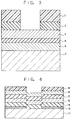
- For generating the bias magnetic field with the anti-ferromagnetic material, there are several restrictions. A first restriction is that it is necessary to form the anti-ferromagnetic layer in direct contact with the ferromagnetic magnetoresistive effect layer since the bias magnetic field is generated with the exchange force. A second restriction is that the anti-ferromagnetic material has to be patterned such as to be present only at opposite end portions of the MR element. This is so because if the exchange force is active over the entire MR element, the response character thereof is deteriorated due to a high anisotropic magnetic field in the inverse magnetic layer. To meet the above two restrictions, as shown in Fig. 3, the ferromagnetic
magnetoresistive effect layer 4 andanti-ferromagnetic layer 3 are formed continuously in vacuum, and then only theanti-ferromagnetic layer 3 is etched. In this patterning, however, it is difficult to selectively etch only theanti-ferromagnetic layer 3. In addition, an over-etching will result in deterioration of the characteristic of the ferromagnetic layer. In Figure 3, designated at 1 is a non-magnetic substrate, at 5 a non-magnetic conductive layer, at 6 electrodes, and at 7 a bias-assistant layer. - On the other hand, Japanese Patent Application No. 124,024/1992 discloses a structure, in which a ground layer is provided only on a portion of an anti-ferromagnetic layer mainly composed of FeMn as shown in Fig. 4. In Fig. 4, designated at 11 is a non-magnetic substrate, at 12 a soft magnetic bias-assistant layer, at 13 a ground layer, at 14 an anti-ferromagnetic layer, at 15 a ferromagnetic magnetoresistive effect layer, at 16 electrodes, and at 17 a non-magnetic conductive layer. The
anti-ferromagnetic layer 14, which is mainly composed of FeMn, has its magnetic characteristics dependent on its crystal structure. While so-called γ phase is an inverse ferromagnetic phase which is stable at room temperature and above, it grows stably only on theground layer 13 having the same face-centered cubic structure. Thus, with the MR head of this structure the same effect as obtainable by patterning theanti-ferromagnetic layer 14 can be obtained by providing theground layer 13 having a face-centered cubic structure only on a desired portion for the bias magnetic field generation with the exchange force. - However, with the structure shown in Fig. 4 it is necessary to provide a non-magnetic
conductive layer 17 for magnetically isolating the ferromagneticmagnetoresistive effect layer 15 and soft magnetic bias-assistant layer 12 from each other, thus complicating the process of manufacture. - An object of the invention is therefore to provide a magnetoresistive head, which is subject to less Barkhausen noise and is simple in structure.
- According to one aspect of the present invention, there is provided a magnetoresistive head comprising a ferromagnetic magnetoresistive effect layer, an anti-ferromagnetic layer for generating a longitudinal bias magnetic field with an exchange force with respect to the ferromagnetic magnetoresistive effect layer, the anti-ferromagnetic layer being provided in direct contact with the ferromagnetic magnetoresistive effect layer and composed of or mainly composed of FeMn, and means for generating a transversal bias magnetic field in the ferromagnetic magnetoresistive effect layer, wherein a ground layer having a face-centered cubic structure is provided on only a portion of said anti-ferromagnetic layer.
- According to another aspect of the present invention, there is provided a magnetoresistive head comprising a ferromagnetic magnetoresistive effect layer, an anti-ferromagnetic layer for generating a longitudinal bias magnetic field by an exchange force with respect to the ferromagnetic magnetoresistive effect layer, and a soft magnetic bias-assistant layer for a transversal bias magnetic field in the ferromagnetic magnetoresistive effect layer, wherein the soft magnetic bias-assistant layer has a crystal structure other than a face-centered cubic structure, a ground layer having a face-centered cubic structure is provided on only a portion of the anti-ferromagnetic layer, and the soft bias-assistant layer, the ground layer, the anti-ferromagnetic layer and the ferromagnetic magnetoresistive effect layer are laminated in the mentioned order.
- Other objects and features will be clarified from the following description with reference to the attached drawings.
-
- Figure 1 shows a sectional view of a magnetoresistive head according to one aspect of the present invention;
- Figure 2 shows a sectional view of a magnetoresistive head according to another aspect of the present invention;
- Figure 3 shows a sectional view of the conventional magnetoresistive head; and
- Figure 4 shows a sectional view of another type of the conventional magnetoresistive head.
- Embodiments of the present invention will now be described with reference to the drawings. Fig. 1 is a sectional view showing an example of the MR head according to the present invention. On a
substrate 1 is formed aground layer 2 having a face-centered cubic structure, and it is patterned to a predetermined shape. On this layer, ananti-ferromagnetic layer 3, a ferromagneticmagnetoresistive effect layer 4, a non-magneticintermediate layer 5 and a bias-assistant layer 6 are laminated in the mentioned order. These laminated layers are patterned to predetermined shapes, and thenelectrodes 7 are formed to the laminate to complete the MR head. - As the material of the
substrate 1 which is a non-magnetic substrate, according to the invention may be used glass, Al₂O₃, TiC, SiC, sintering composed of Al₂O₃ and TiC, ferrite, etc. As theground layer 2 may be used Cu or alloys of NiCr or the like having face-centered cubic structures with or without additives. As the inverseferromagnetic layer 3 may be used anti-ferromagnetic alloys of FeMn, FeMnCr, etc. with or without additives. As the ferromagneticmagnetoresistive effect layer 4 may be used Co, Ni or ferromagnetic alloys, e.g., Ni-Fe, Co-Fe, Co-Ni, etc., with or without additives. As the non-magneticintermediate layer 5 may be used non-magnetic conductive alloys, e.g., Ti, Mo., Cr, Ta, etc. As the bias-assistant layer 6 may be used non-crystalline soft magnetic materials, e.g., CoZr, CoZrNb, CoZrMo, CoZrTa, CoTa, etc. - The anti-ferromagnetic material for generating the longitudinal bias magnetic field and mainly composed of FeMn, has magnetic characteristics dependent on its crystal structure, and the γ phase having a face-centered cubic structure has stable anti-ferromagnetic phase at room temperature or above as stated before. This γ phase is comparatively unstable and can steadily grow only on a ground layer having the same face-centered cubic structure. With the MR head according to the invention the same effect as that of patterning the anti-ferromagnetic layer is obtainable by providing a ground layer having a face-centered cubic structure on only a portion, in which it is desired to generate a bias magnetic field by an exchange coupling force.
- In one experimental example, referring to Fig. 1, a NiCr layer having a thickness of 100 Angstroms was formed as a
ground layer 2 on aglass substrate 1 by a sputtering deposition process. On this layer was formed a predetermined photoresist pattern, and it was ion-etched in an Ar gas atmosphere to obtain two rectangular patterns spaced apart in the longitudinal direction by 10 microns and each having a length of 20 microns and a width of 5 microns. On this photoresist pattern were laminated by the spattering process aFeMn layer 3 having a thickness of 200 Angstroms, a Permalloy layer 4 (82 % Ni-18 % Fe, % being by weight) having a thickness of 400 angstroms, aTi layer 5 having a thickness of 200 Angstroms and aCoZrMo layer 6 having a thickness of 400 Angstroms. On this laminate was formed a predetermined photoresist pattern, which was then ion -etched in an Ar gas atmosphere to a rectangular pattern with a length of 50 microns and a width of 5 microns. At this time, the rectangular pattern was made to overlap the ground layer pattern noted above. - Then,
electrodes 6 for supplying a sense current were formed on the above laminate by using Au, thus completing an element. This element is referred to as Example 1. The electrodes are located at positions of 3 microns from the rectangular pattern center to the opposite sides, and the distance between the electrodes was set to 6 microns. - As Example 2, an MR head was produced in the same process as in Example 1 except for omitting the step of patterning the ground layer. As Example 3, an MR head was produced in the same process as in Example 1 except that the ground layer was not provided. Table 1 shows measurement results of electric resistance versus magnetic field (R-H) curves obtained by applying external field set by causing a sense current of 10 Ma in the above MR heads. As is obvious from the results shown in Table 1, the MR head according to the invention is highly sensitive, free from recognizable Barkhausen noise and has excellent performance.
- As described above, the magnetoresistive head according to the invention comprises a ferromagnetic effect layer, an anti-ferromagnetic layer for generating a longitudinal bias magnetic field with an exchange force with respect to the ferromagnetic magnetoresistive effect layer, the anti-ferromagnetic layer being provided in direct contact with the ferromagnetic magnetoresistive effect layer and composed of or mainly composed of FeMn, and means for generating a transversal bias magnetic field in the ferromagnetic magnetoresistive effect layer, wherein a ground layer having a face-centered cubic structure is provided on only a portion of the anti-ferromagnetic layer. It is thus possible to obtain a magnetoresistive head, which is free from Barkhausen noise.
- Another embodiment of the present invention comprises a soft magnetic bias layer, which has a structure other than a face-centered cubic structure. Thus, a portion of the anti-ferromagnetic layer mainly composed of FeMn that is formed in contact with the soft magnetic bias layer is not magnetic and acts as a layer for magnetically isolating the soft magnetic bias layer and the ferromagnetic magnetoresistive effect layer from each other. This means that there is no need of providing a separate non-magnetic conductive layer for magnetically isolating the ferromagnetic magnetoresistive layer and the soft magnetic bias layer from each other, thus permitting simplification of the process of manufacture. In addition, it is possible to reduce the number of targets by using the same material, e.g., NiFe, for both the ferromagnetic magnetoresistive effect layer and ground layer.
- The invention will further be described in detail with reference to the drawings. Fig. 2 shows an example of the MR head according to the invention. This MR head is produced as follows. First, a soft magnetic bias-
assistant layer 12 is formed on anon-magnetic substrate 11. On this layer is formed aground layer 13 having a face-centered cubic structure, and it is patterned to a predetermined shape. Then, on the patterned ground layer ananti-ferromagnetic layer 14 and a ferromagneticmagnetoresistive effect layer 15 are laminated in the mentioned order. The laminated layers are then patterned to a predetermined shape, and thenelectrodes 16 are provided, thus completing the MR head. - The material used for the
non-magnetic substrate 11 may be glass, Si. Al Al₂O₃, TiC, SiC, sintering composed of Al₂O₃ and TiC, ferrite, etc. The material used for the soft magnetic bias-assistant layer 12 may be non-crystalline soft magnetic materials, e.g., CoZr, CoZrNb,CoZrMo, COZrTa, CoTa, etc. The material used for theground layer 13 may be Cu or an alloy having a face-centered cubic structure, e.g., NiCr, NiFe, etc., with or without additives. The material used for theanti-ferromagnetic layer 14 may be anti-ferromagnetic alloys, e.g., FeMn, FeMcCr, etc., with or without additives. The material used for the ferromagneticmagnetoresistive effect layer 15 may be Co, Ni or a ferromagnetic alloy, e.g., Ni-Fe, Co-Fe, Co-Ni, etc. - The MR head according to the this embodiment was fabricated by the following procedures. On a
glass substrate 11 were laminated a CoZrMo layer with a thickness of 400 Angstroms as softmagnetic bias layer 12 and a NiFe layer with a thickness of 100 Angstroms asground layer 13. On this laminate was formed a predetermined photoresist pattern, and the NiFe layer was then ion-etched in an Ar gas atmosphere into two rectangular patterns spaced apart by 10 microns in the length direction and each having a length of 20 microns and a width of 5 microns. Then, by the sputtering deposition process a FeMn layer with a thickness of 200 Angstroms asanti-ferromagnetic layer 14 and then a Permalloy layer (82 % Ni-18 % Fe, % being by weight) with a thickness of 400 Angstroms as ferromagneticmagnetoresistive effect layer 15 are laminated. Then, on this laminate was formed a predetermined photoresist, which was then ion etched in an Ar gas atmosphere to a rectangular pattern with a length of 50 microns and a width of 5 microns. At this time, the rectangular pattern was made to overlap the pattern of theground layer 13. Thenelectrodes 16 for supplying sense current were provided on the laminate. Theelectrodes 16 were at a distance of 13 microns from the center of the rectangular pattern to the opposite sides, and the distance between the electrodes was set to 6 microns. Thus obtained MR head is referred to as Example 4. - In Example 5, a MR head was produced in the same way as in Example 4 except omission of the step of patterning the
ground layer 13. In Example 6, an MR head was produced in the same way as in Example 4 except for that no ground layer was provided. With the above MR heads, electric resistance versus magnetic field (R-H) curves were measured by applying an external magnetic field by causing a sense current of 10 Ma. The R-H curves serve as an index of the sensitivity of the MR heads, and their half amplitude values and also whether there is Barkhausen noise are shown in Table 2. As is obvious from the results shown in Table 2, the MR head according to the invention is highly sensitive, free from recognizable Barkhausen noise and has excellent performance. - Since in this embodiment NiFe is used for the ferromagnetic magnetoresistive effect layer and ground layer, it is possible to reduce targets. Similar characteristics are of course obtainable by using a different alloy having a face-centered cubic structure for the ground layer.
- With this embodiment of the magnetoresistive head according to the invention, a portion of the anti-ferromagnetic layer with the ground layer provided thereunder may be made to serve as a layer for generating a longitudinal bias magnetic field, and a portion without any ground layer thereunder is made to serve as a layer for magnetically isolating the ferromagnetic magnetoresistive effect layer and the soft magnetic bias layer. It is thus possible to obtain a magnetoresistive head, which is simple, excellent in the reproducibility and free from Barkhausen noise. Besides, the ferromagnetic magnetoresistive effect layer and ground layer may be made of the same material. Further, it is possible to reduce targets.
Claims (13)
- In a magnetoresistive head comprising a ferromagnetic magnetoresistive effect layer, an anti-ferromagnetic layer for generating a longitudinal bias magnetic field with an exchange force with respect to said ferromagnetic magnetoresistive effect layer, said anti-ferromagnetic layer being provided in direct contact with said ferromagnetic magnetoresistive effect layer and composed of or mainly composed of FeMn, and means for generating a transversal bias magnetic field in said ferromagnetic magnetoresistive effect layer, wherein a ground layer having a face-centered cubic structure is provided on only a portion of said anti-ferromagnetic layer.
- The magnetoresistive head according to claim 1, said ground layer is Cu or alloys of NiCr or the like having face-centered cubic structures.
- The magnetoresistive head according to claim 1 or 2, said ferromagnetic magnetoresistive effect layer is Co, Ni or ferromagnetic alloys such as Ni-Fe, Co-Fe, Co-Ni.
- The magnetoresistive head according to any of claims 1 to 3, wherein said anti-ferromagnetic layer is made of FeMn or a material mainly composed of FeMn.
- A magnetoresistive head comprising a ferromagnetic magnetoresistive effect layer, an anti-ferromagnetic layer for generating a longitudinal bias magnetic field by an exchange coupling force with respect to said ferromagnetic magnetoresistive effect layer, and a soft magnetic bias-assistant layer for a transversal bias magnetic field in said ferromagnetic magnetoresistive effect layer, wherein said soft magnetic bias-assistant layer has a crystal structure other than a face-centered cubic structure, a ground layer having a face-centered cubic structure is provided on only a portion of said anti-ferromagnetic layer, and said soft bias-assistant layer, said ground layer, said anti-ferromagnetic layer and said ferromagnetic magnetoresistive effect layer are laminated in the mentioned order.
- The magnetoresistive head according to claim 5, wherein said ferromagnetic magnetoresistive effect layer is of the same material as said ground layer.
- The magnetoresistive head according to claim 5 or 6, wherein said anti-ferromagnetic layer is made of FeMn or a material mainly composed of FeMn.
- The magnetoresistive head according to any of claims 5 to 7, said ground layer is Cu or alloys of NiCr or the like having face-centered cubic structures with or without additives.
- The magnetoresistive head according to any of claims 5 to 8, said anti-ferromagnetic layer is anti-ferromagnetic alloys of FeMn, FeMnCr, etc. with or without additives.
- The magnetoresistive head according to any of claims 5 to 9, said ferromagnetic magnetoresistive effect layer is Co, Ni or ferromagnetic alloys such as Ni-Fe, Co-Fe, Co-Ni, etc., with or without additives.
- The magnetoresistive head according to any of claims 5 to 10, said soft magnetic bias-assistant layer is non-crystalline soft magnetic materials such as CoZr, CoZrNb, CoZrMo, CoZrTa and CoTa.
- In a magnetoresistive element comprising a ferromagnetic magnetoresistive effect layer, an anti-ferromagnetic layer for generating a longitudinal bias magnetic field with an exchange force with respect to said ferromagnetic magnetoresistive effect layer, said anti-ferromagnetic layer being provided in direct contact with said ferromagnetic magnetoresistive effect layer and composed of or mainly composed of FeMn, and means for generating a transversal bias magnetic field in said ferromagnetic magnetoresistive effect layer, wherein a ground layer having a face-centered cubic structure is provided on only a portion of said anti-ferromagnetic layer.
- A magnetoresistive effect element comprising a ferromagnetic magnetoresistive effect layer, an anti-ferromagnetic layer for generating a longitudinal bias magnetic field by an exchange coupling force with respect to said ferromagnetic magnetoresistive effect layer, and a soft magnetic bias-assistant layer for a transversal bias magnetic field in said ferromagnetic magnetoresistive effect layer, wherein said soft magnetic bias-assistant layer has a crystal structure other than a face-centered cubic structure, a ground layer having a face-centered cubic structure is provided on only a portion of said anti-ferromagnetic layer, and said soft bias-assistant layer, said ground layer, said anti-ferromagnetic layer and said ferromagnetic magnetoresistive effect layer are laminated in the mentioned order.
Applications Claiming Priority (4)
| Application Number | Priority Date | Filing Date | Title |
|---|---|---|---|
| JP124024/92 | 1992-05-18 | ||
| JP12402492A JP2800555B2 (en) | 1992-05-18 | 1992-05-18 | Magnetoresistive head |
| JP5026362A JPH07101487B2 (en) | 1993-02-16 | 1993-02-16 | Magnetoresistive head |
| JP26362/93 | 1993-02-16 |
Publications (3)
| Publication Number | Publication Date |
|---|---|
| EP0570883A2 true EP0570883A2 (en) | 1993-11-24 |
| EP0570883A3 EP0570883A3 (en) | 1994-02-23 |
| EP0570883B1 EP0570883B1 (en) | 1998-01-21 |
Family
ID=26364138
Family Applications (1)
| Application Number | Title | Priority Date | Filing Date |
|---|---|---|---|
| EP93108005A Expired - Lifetime EP0570883B1 (en) | 1992-05-18 | 1993-05-17 | A magnetoresistive element |
Country Status (3)
| Country | Link |
|---|---|
| US (1) | US5556718A (en) |
| EP (1) | EP0570883B1 (en) |
| DE (1) | DE69316438T2 (en) |
Cited By (2)
| Publication number | Priority date | Publication date | Assignee | Title |
|---|---|---|---|---|
| DE4401476A1 (en) * | 1993-01-20 | 1994-07-28 | Fuji Electric Co Ltd | Magnetoresistive element serving as thin film magnetic head |
| US5434826A (en) * | 1994-09-26 | 1995-07-18 | Read-Rite Corporation | Multilayer hard bias films for longitudinal biasing in magnetoresistive transducer |
Families Citing this family (8)
| Publication number | Priority date | Publication date | Assignee | Title |
|---|---|---|---|---|
| JPH0845030A (en) * | 1994-08-03 | 1996-02-16 | Alps Electric Co Ltd | Magneto-resistive magnetic head |
| JP2870437B2 (en) * | 1994-12-29 | 1999-03-17 | ヤマハ株式会社 | MR head and method of manufacturing the same |
| US5891586A (en) * | 1995-01-27 | 1999-04-06 | Alps Electric Co., Ltd. | Multilayer thin-film for magnetoresistive device |
| US5796560A (en) * | 1995-03-13 | 1998-08-18 | Kabushiki Kaisha Toshiba | Magnetoresistive head |
| SG40875A1 (en) * | 1995-06-15 | 1997-06-14 | Tdk Corp | Magnetoresistive transducer with spin-valve structure and manufacturing method of the same |
| US5843589A (en) * | 1995-12-21 | 1998-12-01 | Hitachi, Ltd. | Magnetic layered material, and magnetic sensor and magnetic storage/read system based thereon |
| JPH09231523A (en) * | 1996-02-27 | 1997-09-05 | Nec Corp | Magneto-resistive head |
| US5737157A (en) * | 1996-10-09 | 1998-04-07 | International Business Machines Corporation | Disk drive with a thermal asperity reduction circuitry using a magnetoresistive sensor |
Citations (3)
| Publication number | Priority date | Publication date | Assignee | Title |
|---|---|---|---|---|
| EP0265798A2 (en) * | 1986-10-31 | 1988-05-04 | International Business Machines Corporation | A magnetoresistive read transducer |
| EP0288765A2 (en) * | 1987-04-28 | 1988-11-02 | International Business Machines Corporation | Magnetoresistive sensor with mixed phase antiferromagnetic film |
| EP0432890A2 (en) * | 1989-10-31 | 1991-06-19 | International Business Machines Corporation | Magnetoresistive sensor |
Family Cites Families (3)
| Publication number | Priority date | Publication date | Assignee | Title |
|---|---|---|---|---|
| US3864751A (en) * | 1973-10-04 | 1975-02-04 | Ibm | Induced bias magnetoresistive read transducer |
| US4835069A (en) * | 1983-08-06 | 1989-05-30 | Canon Kabushiki Kaisha | Magnetic recording medium |
| US5277991A (en) * | 1991-03-08 | 1994-01-11 | Matsushita Electric Industrial Co., Ltd. | Magnetoresistive materials |
-
1993
- 1993-05-17 EP EP93108005A patent/EP0570883B1/en not_active Expired - Lifetime
- 1993-05-17 DE DE69316438T patent/DE69316438T2/en not_active Expired - Fee Related
- 1993-05-18 US US08/062,221 patent/US5556718A/en not_active Expired - Lifetime
Patent Citations (3)
| Publication number | Priority date | Publication date | Assignee | Title |
|---|---|---|---|---|
| EP0265798A2 (en) * | 1986-10-31 | 1988-05-04 | International Business Machines Corporation | A magnetoresistive read transducer |
| EP0288765A2 (en) * | 1987-04-28 | 1988-11-02 | International Business Machines Corporation | Magnetoresistive sensor with mixed phase antiferromagnetic film |
| EP0432890A2 (en) * | 1989-10-31 | 1991-06-19 | International Business Machines Corporation | Magnetoresistive sensor |
Cited By (2)
| Publication number | Priority date | Publication date | Assignee | Title |
|---|---|---|---|---|
| DE4401476A1 (en) * | 1993-01-20 | 1994-07-28 | Fuji Electric Co Ltd | Magnetoresistive element serving as thin film magnetic head |
| US5434826A (en) * | 1994-09-26 | 1995-07-18 | Read-Rite Corporation | Multilayer hard bias films for longitudinal biasing in magnetoresistive transducer |
Also Published As
| Publication number | Publication date |
|---|---|
| EP0570883A3 (en) | 1994-02-23 |
| DE69316438T2 (en) | 1998-08-27 |
| DE69316438D1 (en) | 1998-02-26 |
| EP0570883B1 (en) | 1998-01-21 |
| US5556718A (en) | 1996-09-17 |
Similar Documents
| Publication | Publication Date | Title |
|---|---|---|
| US6034847A (en) | Apparatus and thin film magnetic head with magnetic membrane layers of different resistivity | |
| US6011674A (en) | Magnetoresistance effect multilayer film with ferromagnetic film sublayers of different ferromagnetic material compositions | |
| US6190764B1 (en) | Inductive write head for magnetic data storage media | |
| JP3990751B2 (en) | Magnetoresistive magnetic head and magnetic recording / reproducing apparatus | |
| JP3022023B2 (en) | Magnetic recording / reproducing device | |
| US6018443A (en) | Thin film magnetic head having hard films for magnetizing a shield layer in a single domain state | |
| US6721147B2 (en) | Longitudinally biased magnetoresistance effect magnetic head and magnetic reproducing apparatus | |
| KR19980042666A (en) | Magnetoresistive element and shielded magnetoresistive effect sensor | |
| US6083632A (en) | Magnetoresistive effect film and method of manufacture thereof | |
| JPH0950613A (en) | Magnetoresistive effect element and magnetic field detecting device | |
| US5556718A (en) | Magnetoresistive head | |
| JPH0778858B2 (en) | Thin film magnetic head | |
| US6120920A (en) | Magneto-resistive effect magnetic head | |
| JPH076329A (en) | Magneto-resistance effect element and magnetic head using the same and magnetic recording and reproducing device | |
| JPH10241125A (en) | Thin film magnetic head and recording/reproducing separation type magnetic head and magnetic recording/ reproducing apparatus using the same | |
| JP2800555B2 (en) | Magnetoresistive head | |
| Jayasekara et al. | Inductive write heads using high moment FeAlN poles | |
| JPH05250642A (en) | Magnetoresist effect sensor | |
| JP2661068B2 (en) | Magnetoresistive magnetic head | |
| JPS63129511A (en) | Magnetoresistance effect type thin film magnetic head | |
| JP2861714B2 (en) | Magnetoresistive head and magnetic disk drive | |
| JPH0782612B2 (en) | Thin film magnetic head and method of manufacturing the same | |
| JPS63138515A (en) | Thin film magnetic head and its reproduction system | |
| JPS5987616A (en) | Magnetic thin film head | |
| JPH06243435A (en) | Magnetoresistive effect head |
Legal Events
| Date | Code | Title | Description |
|---|---|---|---|
| PUAI | Public reference made under article 153(3) epc to a published international application that has entered the european phase |
Free format text: ORIGINAL CODE: 0009012 |
|
| AK | Designated contracting states |
Kind code of ref document: A2 Designated state(s): DE FR GB NL |
|
| PUAL | Search report despatched |
Free format text: ORIGINAL CODE: 0009013 |
|
| AK | Designated contracting states |
Kind code of ref document: A3 Designated state(s): DE FR GB NL |
|
| 17P | Request for examination filed |
Effective date: 19940112 |
|
| 17Q | First examination report despatched |
Effective date: 19960809 |
|
| GRAG | Despatch of communication of intention to grant |
Free format text: ORIGINAL CODE: EPIDOS AGRA |
|
| GRAG | Despatch of communication of intention to grant |
Free format text: ORIGINAL CODE: EPIDOS AGRA |
|
| GRAG | Despatch of communication of intention to grant |
Free format text: ORIGINAL CODE: EPIDOS AGRA |
|
| GRAH | Despatch of communication of intention to grant a patent |
Free format text: ORIGINAL CODE: EPIDOS IGRA |
|
| GRAH | Despatch of communication of intention to grant a patent |
Free format text: ORIGINAL CODE: EPIDOS IGRA |
|
| GRAA | (expected) grant |
Free format text: ORIGINAL CODE: 0009210 |
|
| AK | Designated contracting states |
Kind code of ref document: B1 Designated state(s): DE FR GB NL |
|
| REF | Corresponds to: |
Ref document number: 69316438 Country of ref document: DE Date of ref document: 19980226 |
|
| ET | Fr: translation filed | ||
| PLBE | No opposition filed within time limit |
Free format text: ORIGINAL CODE: 0009261 |
|
| STAA | Information on the status of an ep patent application or granted ep patent |
Free format text: STATUS: NO OPPOSITION FILED WITHIN TIME LIMIT |
|
| 26N | No opposition filed | ||
| REG | Reference to a national code |
Ref country code: GB Ref legal event code: IF02 |
|
| REG | Reference to a national code |
Ref country code: GB Ref legal event code: 732E |
|
| NLS | Nl: assignments of ep-patents |
Owner name: TDK CORPORATION |
|
| PGFP | Annual fee paid to national office [announced via postgrant information from national office to epo] |
Ref country code: FR Payment date: 20030508 Year of fee payment: 11 |
|
| PGFP | Annual fee paid to national office [announced via postgrant information from national office to epo] |
Ref country code: GB Payment date: 20030514 Year of fee payment: 11 |
|
| PGFP | Annual fee paid to national office [announced via postgrant information from national office to epo] |
Ref country code: DE Payment date: 20030529 Year of fee payment: 11 |
|
| PGFP | Annual fee paid to national office [announced via postgrant information from national office to epo] |
Ref country code: NL Payment date: 20030530 Year of fee payment: 11 |
|
| REG | Reference to a national code |
Ref country code: FR Ref legal event code: TP |
|
| PG25 | Lapsed in a contracting state [announced via postgrant information from national office to epo] |
Ref country code: GB Free format text: LAPSE BECAUSE OF NON-PAYMENT OF DUE FEES Effective date: 20040517 |
|
| PG25 | Lapsed in a contracting state [announced via postgrant information from national office to epo] |
Ref country code: NL Free format text: LAPSE BECAUSE OF NON-PAYMENT OF DUE FEES Effective date: 20041201 Ref country code: DE Free format text: LAPSE BECAUSE OF NON-PAYMENT OF DUE FEES Effective date: 20041201 |
|
| GBPC | Gb: european patent ceased through non-payment of renewal fee |
Effective date: 20040517 |
|
| PG25 | Lapsed in a contracting state [announced via postgrant information from national office to epo] |
Ref country code: FR Free format text: LAPSE BECAUSE OF NON-PAYMENT OF DUE FEES Effective date: 20050131 |
|
| NLV4 | Nl: lapsed or anulled due to non-payment of the annual fee |
Effective date: 20041201 |
|
| REG | Reference to a national code |
Ref country code: FR Ref legal event code: ST |