EP0567408B1 - Device for supplying discharge lamps and automotive headlamp containing such a device - Google Patents
Device for supplying discharge lamps and automotive headlamp containing such a device Download PDFInfo
- Publication number
- EP0567408B1 EP0567408B1 EP93401064A EP93401064A EP0567408B1 EP 0567408 B1 EP0567408 B1 EP 0567408B1 EP 93401064 A EP93401064 A EP 93401064A EP 93401064 A EP93401064 A EP 93401064A EP 0567408 B1 EP0567408 B1 EP 0567408B1
- Authority
- EP
- European Patent Office
- Prior art keywords
- voltage
- transformer
- circuit
- interruptor
- terminals
- Prior art date
- Legal status (The legal status is an assumption and is not a legal conclusion. Google has not performed a legal analysis and makes no representation as to the accuracy of the status listed.)
- Expired - Lifetime
Links
Images


Classifications
-
- H—ELECTRICITY
- H05—ELECTRIC TECHNIQUES NOT OTHERWISE PROVIDED FOR
- H05B—ELECTRIC HEATING; ELECTRIC LIGHT SOURCES NOT OTHERWISE PROVIDED FOR; CIRCUIT ARRANGEMENTS FOR ELECTRIC LIGHT SOURCES, IN GENERAL
- H05B41/00—Circuit arrangements or apparatus for igniting or operating discharge lamps
- H05B41/14—Circuit arrangements
- H05B41/36—Controlling
- H05B41/38—Controlling the intensity of light
-
- H—ELECTRICITY
- H05—ELECTRIC TECHNIQUES NOT OTHERWISE PROVIDED FOR
- H05B—ELECTRIC HEATING; ELECTRIC LIGHT SOURCES NOT OTHERWISE PROVIDED FOR; CIRCUIT ARRANGEMENTS FOR ELECTRIC LIGHT SOURCES, IN GENERAL
- H05B41/00—Circuit arrangements or apparatus for igniting or operating discharge lamps
- H05B41/14—Circuit arrangements
- H05B41/26—Circuit arrangements in which the lamp is fed by power derived from dc by means of a converter, e.g. by high-voltage dc
- H05B41/28—Circuit arrangements in which the lamp is fed by power derived from dc by means of a converter, e.g. by high-voltage dc using static converters
- H05B41/288—Circuit arrangements in which the lamp is fed by power derived from dc by means of a converter, e.g. by high-voltage dc using static converters with semiconductor devices and specially adapted for lamps without preheating electrodes, e.g. for high-intensity discharge lamps, high-pressure mercury or sodium lamps or low-pressure sodium lamps
- H05B41/2881—Load circuits; Control thereof
- H05B41/2882—Load circuits; Control thereof the control resulting from an action on the static converter
-
- H—ELECTRICITY
- H05—ELECTRIC TECHNIQUES NOT OTHERWISE PROVIDED FOR
- H05B—ELECTRIC HEATING; ELECTRIC LIGHT SOURCES NOT OTHERWISE PROVIDED FOR; CIRCUIT ARRANGEMENTS FOR ELECTRIC LIGHT SOURCES, IN GENERAL
- H05B41/00—Circuit arrangements or apparatus for igniting or operating discharge lamps
- H05B41/14—Circuit arrangements
- H05B41/26—Circuit arrangements in which the lamp is fed by power derived from dc by means of a converter, e.g. by high-voltage dc
- H05B41/28—Circuit arrangements in which the lamp is fed by power derived from dc by means of a converter, e.g. by high-voltage dc using static converters
- H05B41/288—Circuit arrangements in which the lamp is fed by power derived from dc by means of a converter, e.g. by high-voltage dc using static converters with semiconductor devices and specially adapted for lamps without preheating electrodes, e.g. for high-intensity discharge lamps, high-pressure mercury or sodium lamps or low-pressure sodium lamps
- H05B41/2885—Static converters especially adapted therefor; Control thereof
- H05B41/2886—Static converters especially adapted therefor; Control thereof comprising a controllable preconditioner, e.g. a booster
-
- H—ELECTRICITY
- H05—ELECTRIC TECHNIQUES NOT OTHERWISE PROVIDED FOR
- H05B—ELECTRIC HEATING; ELECTRIC LIGHT SOURCES NOT OTHERWISE PROVIDED FOR; CIRCUIT ARRANGEMENTS FOR ELECTRIC LIGHT SOURCES, IN GENERAL
- H05B41/00—Circuit arrangements or apparatus for igniting or operating discharge lamps
- H05B41/14—Circuit arrangements
- H05B41/26—Circuit arrangements in which the lamp is fed by power derived from dc by means of a converter, e.g. by high-voltage dc
- H05B41/28—Circuit arrangements in which the lamp is fed by power derived from dc by means of a converter, e.g. by high-voltage dc using static converters
- H05B41/288—Circuit arrangements in which the lamp is fed by power derived from dc by means of a converter, e.g. by high-voltage dc using static converters with semiconductor devices and specially adapted for lamps without preheating electrodes, e.g. for high-intensity discharge lamps, high-pressure mercury or sodium lamps or low-pressure sodium lamps
- H05B41/2885—Static converters especially adapted therefor; Control thereof
- H05B41/2887—Static converters especially adapted therefor; Control thereof characterised by a controllable bridge in the final stage
- H05B41/2888—Static converters especially adapted therefor; Control thereof characterised by a controllable bridge in the final stage the bridge being commutated at low frequency, e.g. 1kHz
-
- Y—GENERAL TAGGING OF NEW TECHNOLOGICAL DEVELOPMENTS; GENERAL TAGGING OF CROSS-SECTIONAL TECHNOLOGIES SPANNING OVER SEVERAL SECTIONS OF THE IPC; TECHNICAL SUBJECTS COVERED BY FORMER USPC CROSS-REFERENCE ART COLLECTIONS [XRACs] AND DIGESTS
- Y02—TECHNOLOGIES OR APPLICATIONS FOR MITIGATION OR ADAPTATION AGAINST CLIMATE CHANGE
- Y02B—CLIMATE CHANGE MITIGATION TECHNOLOGIES RELATED TO BUILDINGS, e.g. HOUSING, HOUSE APPLIANCES OR RELATED END-USER APPLICATIONS
- Y02B20/00—Energy efficient lighting technologies, e.g. halogen lamps or gas discharge lamps
-
- Y—GENERAL TAGGING OF NEW TECHNOLOGICAL DEVELOPMENTS; GENERAL TAGGING OF CROSS-SECTIONAL TECHNOLOGIES SPANNING OVER SEVERAL SECTIONS OF THE IPC; TECHNICAL SUBJECTS COVERED BY FORMER USPC CROSS-REFERENCE ART COLLECTIONS [XRACs] AND DIGESTS
- Y10—TECHNICAL SUBJECTS COVERED BY FORMER USPC
- Y10S—TECHNICAL SUBJECTS COVERED BY FORMER USPC CROSS-REFERENCE ART COLLECTIONS [XRACs] AND DIGESTS
- Y10S315/00—Electric lamp and discharge devices: systems
- Y10S315/07—Starting and control circuits for gas discharge lamp using transistors
Definitions
- the present invention relates to a device for supplying discharge lamps, in particular intended to equip a vehicle headlight.
- the invention also relates to a vehicle lighting system equipped with such a device.
- document EP-A-0 477 587 proposes a supply diagram around an assembly called half-bridge which uses only two switches.
- Document DE-A-40 33 664 also teaches a method for controlling such switches.
- the circuit described in document EP-A-0 477 587 is supplied by an alternating voltage generator device. It further comprises a device for igniting the discharge lamp powered by another generator device.
- a separate generator device for the ignition circuit is not acceptable in a device intended for a vehicle headlamp.
- An advantage of the present invention is thus to create a priming device without requiring a second generator.
- provision is made to switch from priming mode to maintenance mode by changing the frequency, which represents a great simplification compared to the devices of the prior art.
- the alternating voltage generator device comprises a quasi-resonant voltage switch and its output is constituted by at least one transformer secondary.
- the rectifier device comprises at least one series circuit consisting of a diode and a capacitor.
- the rectifier device comprises two aforementioned series circuits
- this is an advantage of the invention compared to a conventional half-bridge assembly. than charging the two capacitors simultaneously.
- these are loaded in series and must be sized according to the cutting frequency of the half-bridge (low to be able to use semiconductor components like IGBTs which are slow and to avoid generate electromagnetic interference with the connecting wires between the supply device and the discharge lamp.
- the capacitors of the rectifier device filter the outputs of the quasi-resonant converter whose chopping frequency can reach 1 MHz (10 6 Hz).
- the capacity of these capacitors can be low (of the order of 1000 times lower than that of the capacitors of a conventional half-bridge).
- the invention also relates to a vehicle headlight fitted with such a power supply device.
- the supply device of the invention comprises a means making it possible to produce an alternating high voltage.
- this means is constituted by a quasi-resonant inverter in voltage.
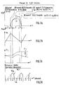
- the supply device comprises a transformer Tr whose primary PRIM comprises a winding of n1 turns and has a leakage inductance of value Lm.
- the secondary SEC of the transformer Tr comprises a plurality of windings En1, En2, En3, ... comprising n2 and n3 turns.
- the directions of the windings are identical and shown in Figure 1 by dots.
- the foot of the primary winding PRIM is connected to a switch I0 of the quasi-resonant type, which comprises a switching element K0 whose control electrode 1 is connected to the output of a control device 4.
- the switch I0 forms a quasi-resonant switch with the transformer.
- the control device 4 manages, according to a recorded program, the switching phases of the various switches of the device of the invention, as a function of parameters measured by known means 5 at the input of the control device 4.
- an analog type control circuit comprises an analog type control circuit.
- the parameters measured by means 5 are the instantaneous current and voltage which pass through the LAD lamp.
- the quasi-resonant switch consists of an embodiment by a parallel circuit composed of a controlled switch K0, by a diode D0 and a capacitor C0 and is designed to operate on high switching frequencies of the order of 100 KHz and more.
- control electrode 1 is connected to a suitable output of the control device 4.
- the power supply device is built around a half-bridge located at the secondary SEC of the pulse transformer Tr and constituted by two controlled switches K1 and K2.
- each switch K1, K2 is doubled by a diode D4 or D5.
- the diode is constituted by the diode induced between source and drain.
- the common point M between the two controlled switches K1 and K2 is connected to a first terminal of at least one discharge lamp LAD, a second terminal of which is connected to a rectifier device 400 of at least one alternation of the high alternating voltage produced at the secondary S of the transformer Tr.
- the device 400 has a pair of output terminals B1, B3.
- a first output terminal B1 of the device 400 is connected to a first end of the series circuit constituted by the two switches K1 and K2, while a second output terminal B3 of the device 400 is connected to a second end of the series circuit constituted by the two switches K1 and K2.
- the rectifier device 400 includes an output terminal B2 connected to the other end of the discharge lamp LAD.
- the supply device also includes a priming circuit 200 formed around an ECL spark gap.
- a spark gap is constituted by a discharge tube, the ignition voltage of which is lower and easier to reach than that of the LAD discharge lamp intended, for its part, to produce a luminous flux having as fast as possible a suitable luminous efficiency.
- the Ecl spark gap has two connection terminals.
- the first terminal 6a is connected to a terminal of a winding L2 of a second transformer Tr 'and the second terminal 6b is connected to a terminal B5 of the rectifier device 400.
- the other terminal of the primary winding L2 is directly connected to an output terminal B4 of the rectifier device 400.
- the rectifier device consists of a series of single-wave rectifier cells, each cell comprising a diode and a capacitor; like cells D1, C1, D2, C2 and D3, C3.
- the transformer Tr has an inductive leakage characteristic L at the primary which is taken into account in the operation of the quasi-resonant switch.
- a coil of suitable predetermined value L can be added to the primary circuit, in series with the primary winding PRIM.
- the supply circuit of the invention is therefore composed with a quasi-resonant switch only placed at the primary of the transformer and with two simple switches at the secondary SEC.
- One of the advantages of the invention lies in the possibility of creating an initiating device or means without requiring a secondary inverter. Thanks to the quasi-resonant converter, a simple change of frequency makes it possible to switch from the priming mode (frequency low) which makes it possible to reach between terminals B4 and B5 a voltage greater than the spark gap ignition threshold in maintenance mode (higher frequency).
- FIG 2 there is shown an equivalent diagram of the power circuit when the LAD lamp is off.
- the Ecl spark gap in Figure 1 is assumed to be blocked.
- the supply circuit comprises at the primary of Tr the PRIM winding, the quasi-resonant switch and the DC voltage source E, for example constituted by the battery on board the vehicle.
- the rectifying device 400 consisting of the three cells C1, D1, C2, D2 and C3, D3. At the terminals of capacitors C1 to C3, the instantaneous voltages are measured.
- an equivalent diode D123 has been formed with the three diodes of the above-mentioned cells D1, D2 and D3 .
- FIG 4 there is shown a diagram during the first supply phase in boot mode starting from the state of Figure 2.
- the switch K0 is closed, the diode D123 is blocked, the current flowing the primary winding Lm, ie the current im, is initially negative (see Figure 7a).
- the current i is a linearly increasing current (see phase 1, Figure 7b).
- the control circuit 4 detects, using a special current measuring means, that the current i is sufficiently large and switches the switch K0 by its control electrode 1 ( Figure 1).
- the control device 4 does not measure any particular parameter other than the predetermined phase switching time 1 for a given supply device, and switches the switch after this predetermined time.
- the voltage across the capacitor C0 is zero (see phase 1, Figure 7a), and the magnetic circuit of Tr stores magnetic energy.
- Phase 2 ends naturally when the voltage across the winding Lm becomes low enough for the diode D123 to turn on again.
- the diode D123 being produced by switches controlled in place of the diodes D1, D2 or D3, may become conducting under the control of the piloting or control circuit 4, as a function of measurements carried out by a particular means whose realization is within the reach of the skilled person.
- phase 3 the switch K0 is open, diode D123 is conducting, the magnetizing current im is positive, the voltage VC0 across the capacitor C0 is positive (see phase 3, Figure 7a).
- the equivalent diagram is given in FIG. 6, in which, the diode 123 being on, the equivalent capacitor Ceq is connected to the terminals of the coil Lm.
- This end can be controlled in the aforementioned embodiment not shown, for example as a function of the characteristics of the desired light flux produced by the LAD discharge lamp as a function of the measurements taken on the measurement means 5 connected at the input of the control circuit 4 .
- phase 4 ends naturally when the diode D0 of the quasi-resonant switch becomes conductive again. Therefore, the current im will have to increase, and it will be necessary to close quickly the switch K0 before im becomes positive again.
- FIGS. 8 to 13 the same operation is shown with a lit LAD lamp, which then constitutes, in particular if the thermal regime of the LAD lamp is well established, a resistive load for the supply device.
- the switch K0 works as in the case of the LAD lamp off operation.
- the equivalent diode DE1 shown in FIG. 9 follows the same on-off states as the equivalent diode D123.
- the switch K0 is closed, the diode DE1 is blocked, the current im in the winding Lm is negative and the voltage VC1 at the terminals of the capacitor C1 is positive . Therefore, the capacitor C1 discharges in the series circuit constituted by the equivalent choke L / m 2 of the transformer Tr 'of ignition and in the equivalent resistance R / m 2 of the lamp LAD.
- the control circuit 4 measures the current in the winding Lm and opens the switch K0 when the value of the current im flowing through it has become sufficiently positive (see phase 1, Figure 7b). In another embodiment, the control circuit 4 imposes a duration of conduction and a duration of opening of the switch K0 and the speed is established by itself.
- the switch K0 is open, the diode DE1 is blocked, the current im in the coil Lm is positive and the voltage VC0 across the capacitor C0 is still zero.
- phase 2 is a simple extension of phase 1 with the introduction of the capacitor C0 in the left loop of the diagram in Figure 11.
- the curve representing the current im in the winding Lm is shown in dashed lines and in solid lines the curve representative of the voltage VC0 across the terminals of the capacitor C0, when the voltage VC1 across the terminals of the capacitor C1 has reached a maximum value at which it remains blocked.
- the incoming energy but not consumed in the converter is restored on the source E.
- This operating mode can appear in certain cases of breakdowns or displacement of the adjustment points (due for example to the aging of the components, etc.).
- the invention has the advantage of then proposing a non-dissipative and non-destructive operating mode since the voltages then remain below the trigger threshold of the spark gap.
- the spark gap starts during phase 3 during no-load operation after a few thousand periods during which it remains off.
- the diodes D1 and D2 can be mounted in opposite directions to each other, if for example the diode D1 is mounted at the head of the winding En1, that the foot of the winding En1 is connected at series with the head of the winding En2 and that the diode D2 is connected to the foot of the winding En2.
- the switches of the three switches which are the basis of the invention are managed by the control device 4 using the measurements of the means 5.
- the two switches K1, K2 of the half-bridge operate independently of the switches of the quasi-resonant switch I0 and in phase opposition with respect to each other. Their control electrodes are activated by the control device 4.
- the switching frequency of these switches is determined to be much lower than that of K0. Therefore, the operation of the supply device consists of a succession of regimes established with a periodic change in the direction of the voltage delivered, change produced by the switching of the half-bridge.
- the ignition which has been described in the present application can be carried out with other devices generating a high voltage than a spark gap.
- a semiconductor component can be used.
- rectifier devices can be modified and take any other structure compatible with the described operation.
Description
La présente invention concerne un dispositif d'alimentation de lampes à décharge, notamment destiné à équiper un projecteur de véhicule. L'invention concerne aussi un système d'éclairage de véhicule équipé d'un tel dispositif.The present invention relates to a device for supplying discharge lamps, in particular intended to equip a vehicle headlight. The invention also relates to a vehicle lighting system equipped with such a device.
Dans l'art antérieur, on a déjà proposé des dispositifs permettant de produire une première tension alternative de valeur élevée destinée à l'amorçage de la lampe à décharge. Puis, une fois la lampe allumée, le dispositif d'alimentation génère une tension alternative de faible valeur.In the prior art, devices have already been proposed making it possible to produce a first high-voltage alternating voltage intended for starting the discharge lamp. Then, once the lamp is on, the supply device generates an AC voltage of low value.
En particulier, on a déjà proposé un schéma d'alimentation constitué autour d'un montage dénommé pont en "H". Mais un tel dispositif exige quatre interrupteurs pour l'ensemble des branches du pont, la lampe à décharge se trouvant placée dans la branche centrale du pont. Or ces interrupteurs peuvent être traversés par de forts courants. De ce fait, ces composants sont chers car ils doivent présenter peu de pertes à l'état passant puisqu'à un instant donné deux interrupteurs fermés sont en série avec la charge.In particular, a power supply scheme has already been proposed around a circuit called "H" bridge. However, such a device requires four switches for all the branches of the bridge, the discharge lamp being placed in the central branch of the bridge. However, these switches can be crossed by strong currents. Therefore, these components are expensive because they must have few losses in the on state since at a given time two closed switches are in series with the load.
Afin de réduire ces inconvénients, le document EP-A-0 477 587 propose un schéma d'alimentation autour d'un montage dénommé demi-pont qui n'utilise que deux interrupteurs. Le document DE-A-40 33 664 enseigne d'ailleurs un procédé de commande de tels interrupteurs.In order to reduce these drawbacks, document EP-A-0 477 587 proposes a supply diagram around an assembly called half-bridge which uses only two switches. Document DE-A-40 33 664 also teaches a method for controlling such switches.
Le circuit décrit dans le document EP-A-0 477 587 est alimenté par un dispositif générateur de tension alternative. Il comprend en outre un dispositif d'amorçage de la lampe à décharge alimenté par un autre dispositif générateur. L'utilisation d'un dispositif générateur distinct pour le circuit d'amorçage n'est pas acceptable dans un dispositif destiné à un projecteur de véhicule.The circuit described in document EP-A-0 477 587 is supplied by an alternating voltage generator device. It further comprises a device for igniting the discharge lamp powered by another generator device. The use of a separate generator device for the ignition circuit is not acceptable in a device intended for a vehicle headlamp.
Pour remédier à ces inconvénients de l'art antérieur, la présente invention propose un dispositif d'alimentation de lampes à décharge, du type comprenant :
- un dispositif générateur de tension alternative comprenant un premier transformateur,
- une première partie d'un dispositif redresseur connecté à au moins un enroulement secondaire dudit premier transformateur , ladite première partie du dispositif redresseur présentant une première et une deuxième bornes de sortie et une troisième borne maintenue à un potentiel intermédiaire par rapport à celui desdites première et deuxième bornes de sortie,
- deux interrupteurs connectés en série auxdites première et deuxième bornes de sortie,
- un circuit d'amorçage comprenant un second transformateur dont le secondaire constitue le dipôle de sortie dudit circuit d'amorçage,
caractérisé en ce qu'une deuxième partie du dispositif redresseur est connecté à un autre enroulement secondaire du premier transformateur et présente deux bornes qui constituent les bornes d'entrée du circuit d'amorçage.To remedy these drawbacks of the prior art, the present invention provides a device for supplying discharge lamps, of the type comprising:
- an alternating voltage generator device comprising a first transformer,
- a first part of a connected rectifier device at least one secondary winding of said first transformer, said first part of the rectifier device having first and second output terminals and a third terminal maintained at an intermediate potential with respect to that of said first and second output terminals,
- two switches connected in series to said first and second output terminals,
- an ignition circuit comprising a second transformer, the secondary of which constitutes the output dipole of said ignition circuit,
characterized in that a second part of the rectifier device is connected to another secondary winding of the first transformer and has two terminals which constitute the input terminals of the ignition circuit.
Un avantage de la présente invention est ainsi de créer un dispositif d'amorçage sans nécessiter un second générateur.An advantage of the present invention is thus to create a priming device without requiring a second generator.
Dans un mode de réalisation, il est prévu de passer du mode d'amorçage au mode d'entretien par un changement de fréquence, ce qui représente une grande simplification par rapport aux dispositifs de l'art antérieur.In one embodiment, provision is made to switch from priming mode to maintenance mode by changing the frequency, which represents a great simplification compared to the devices of the prior art.
Dans un mode de réalisation, le dispositif générateur de tension alternative comprend un interrupteur quasi-résonnant en tension et sa sortie est constituée par au moins un secondaire de transformateur.In one embodiment, the alternating voltage generator device comprises a quasi-resonant voltage switch and its output is constituted by at least one transformer secondary.
Dans un mode de réalisation, le dispositif redresseur comporte au moins un circuit série constitué d'une diode et d'un condensateur.In one embodiment, the rectifier device comprises at least one series circuit consisting of a diode and a capacitor.
Quand le dispositif redresseur comporte deux circuits série précités, c'est un avantage de l'invention par rapport à un montage classique à demi-pont que de charger simultanément les deux condensateurs. Dans un demi- pont classique, ceux-ci sont chargés en série et doivent être dimensionnés en fonction de la fréquence de découpage du demi-pont (basse pour pouvoir utiliser des composants semi-conducteurs comme des IGBT qui sont lents et pour éviter d'engendrer des perturbations électromagnétiques avec les fils de liaison entre le dispositif d'alimentation et la lampe à décharge.When the rectifier device comprises two aforementioned series circuits, this is an advantage of the invention compared to a conventional half-bridge assembly. than charging the two capacitors simultaneously. In a conventional half-bridge, these are loaded in series and must be sized according to the cutting frequency of the half-bridge (low to be able to use semiconductor components like IGBTs which are slow and to avoid generate electromagnetic interference with the connecting wires between the supply device and the discharge lamp.
Dans l'invention, les condensateurs du dispositif redresseur filtrent les sorties du convertisseur quasi-résonnant dont la fréquence de découpage peut atteindre 1 Mhz (106 Hz). La capacité de ces condensateurs peut être faible ( de l'ordre de 1000 fois plus faible que celle des condensateurs d'un demi-pont classique).In the invention, the capacitors of the rectifier device filter the outputs of the quasi-resonant converter whose chopping frequency can reach 1 MHz (10 6 Hz). The capacity of these capacitors can be low (of the order of 1000 times lower than that of the capacitors of a conventional half-bridge).
L'invention concerne aussi un projecteur de véhicule équipé d'un tel dispositif d'alimentation.The invention also relates to a vehicle headlight fitted with such a power supply device.
D'autres caractéristiques et avantages de la présente invention seront mieux compris à l'aide de la description et des figures annexées qui sont :
- La figure 1 : un schéma d'un premier mode de réalisation de la présente invention ;
- Les figures 2 à 6 : des schémas équivalents du circuit de la figure 1 expliquant le fonctionnement à lampe éteinte du mode de réalisation de la présente invention ;
- Les figures 7a à 7d : des graphes des courants et tensions en divers points du dispositif représenté aux figures 1 à 6 ;
- Les figures 8 à 13 : des schémas équivalents du circuit de la figure 1 expliquant le fonctionnement à lampe allumée du mode de réalisation de la présente invention avec référence aux figures 7a à 7d ;
- La figure 14 : un schéma équivalent d'amorçage du dispositif selon l'invention ;
- Les figures 15a et 15b : des graphes des courants et tensions en divers points du dispositif représenté notamment par la figure 14.
- Figure 1: a diagram of a first embodiment of the present invention;
- FIGS. 2 to 6: equivalent diagrams of the circuit of FIG. 1 explaining the operation with the lamp off of the embodiment of the present invention;
- Figures 7a to 7d: graphs of currents and voltages at various points in the device shown in Figures 1 to 6;
- FIGS. 8 to 13: equivalent diagrams of the circuit of FIG. 1 explaining the operation with a lit lamp of the embodiment of the present invention with reference to FIGS. 7a to 7d;
- Figure 14: an equivalent boot diagram of the device according to the invention;
- Figures 15a and 15b: graphs of currents and voltages at various points of the device shown in particular in FIG. 14.
A la figure 1, on a représenté un schéma d'un premier mode de réalisation de la présente invention.In Figure 1, there is shown a diagram of a first embodiment of the present invention.
A la figure 1, le dispositif d'alimentation de l'invention comporte un moyen permettant de produire une haute tension alternative. Dans un mode préféré de réalisation, ce moyen est constitué par un onduleur quasi-résonnant en tension.In FIG. 1, the supply device of the invention comprises a means making it possible to produce an alternating high voltage. In a preferred embodiment, this means is constituted by a quasi-resonant inverter in voltage.
A cet effet, le dispositif d'alimentation selon l'invention comporte un transformateur Tr dont le primaire PRIM comporte un enroulement de n1 spires et présente une inductance de fuite de valeur Lm. Le secondaire SEC du transformateur Tr comporte une pluralité d'enroulements En1, En2, En3, ... comportant n2 et n3 spires. Les sens des enroulements sont identiques et figurés à la figure 1 par des points.To this end, the supply device according to the invention comprises a transformer Tr whose primary PRIM comprises a winding of n1 turns and has a leakage inductance of value Lm. The secondary SEC of the transformer Tr comprises a plurality of windings En1, En2, En3, ... comprising n2 and n3 turns. The directions of the windings are identical and shown in Figure 1 by dots.
Le pied de l'enroulement primaire PRIM est connecté à un interrupteur I0 du type quasi-résonnant, qui comporte un élément de commutation K0 dont l'électrode de commande 1 est connectée à la sortie d'un dispositif de commande 4. L'interrrupteur I0 forme un interrupteur quasi-résonnant avec le transformateur. Le dispositif de commande 4 gère selon un programme enregistré les phases de commutation des divers interrupteurs du dispositif de l'invention, en fonction de paramètres mesurés par un moyen connu 5 en entrée du dispositif de commande 4. Dans un autre mode de réalisation adapté à la présente description, et dont l'exécution en suivant la divugation de la présente demande est à la portée de l'homme de métier, comporte un circuit de commande de type analogique.The foot of the primary winding PRIM is connected to a switch I0 of the quasi-resonant type, which comprises a switching element K0 whose
Dans un mode de réalisation préféré, les paramètres mesurés par le moyen 5 sont le courant et la tension instantanés qui traversent la lampe LAD.In a preferred embodiment, the parameters measured by means 5 are the instantaneous current and voltage which pass through the LAD lamp.
L'interrupteur quasi-résonnant est constitué dans un mode de réalisation par un circuit parallèle composé d'un interrupteur commandé K0, par une diode D0 et un condensateur C0 et est prévu pour fonctionner sur des hautes fréquences de commutation de l'ordre de 100 KHz et plus.The quasi-resonant switch consists of an embodiment by a parallel circuit composed of a controlled switch K0, by a diode D0 and a capacitor C0 and is designed to operate on high switching frequencies of the order of 100 KHz and more.
A cet effet, l'électrode de commande 1 est connectée à une sortie convenable du dispositif de commande 4.To this end, the
Le dispositif d'alimentation est construit autour d'un demi-pont disposé au secondaire SEC du transformateur impulsionnel Tr et constitué par deux interrupteurs commandés K1 et K2. Dans le cas où le composant servant à réaliser ne comporte pas de diode anti-parallèle dans son chemin de commutation (cas d'un composant IGBT), chaque interrupteur K1, K2 est doublé par une diode D4 ou D5. En particulier, dans le cas où les interrupteurs sont constitués par des transistors à effet de champ de puissance, la diode est constituée par la diode induite entre source et drain.The power supply device is built around a half-bridge located at the secondary SEC of the pulse transformer Tr and constituted by two controlled switches K1 and K2. In the case where the component used to produce does not have an anti-parallel diode in its switching path (case of an IGBT component), each switch K1, K2 is doubled by a diode D4 or D5. In particular, in the case where the switches are constituted by power field effect transistors, the diode is constituted by the diode induced between source and drain.
Le point commun M entre les deux interrupteurs commandés K1 et K2 est connecté à une première borne d'au moins une lampe à décharge LAD, dont une seconde borne est connectée à un dispositif redresseur 400 d'au moins une alternance de la haute tension alternative produite au secondaire S du transformateur Tr. Le dispositif 400 présente une paire de bornes de sortie B1, B3. Une première borne de sortie B1 du dispositif 400 est connectée à une première extrémité du circuit série constitué par les deux interrupteurs K1 et K2, tandis qu'une seconde borne de sortie B3 du dispositif 400 est connectée à une seconde extrémité du circuit série constitué par les deux interrupteurs K1 et K2.The common point M between the two controlled switches K1 and K2 is connected to a first terminal of at least one discharge lamp LAD, a second terminal of which is connected to a
Enfin, le dispositif redresseur 400 comporte une borne de sortie B2 connectée à l'autre extrémité de la lampe à décharge LAD.Finally, the
Dans un mode de réalisation préféré, le dispositif d'alimentation comporte aussi un circuit d'amorçage 200 constitué autour d'un éclateur ECL.In a preferred embodiment, the supply device also includes a
Un éclateur est constitué par un tube à décharge dont la tension d'amorçage est plus basse et plus facile à atteindre que celle de la lampe à décharge LAD destinée, elle, à produire un flux lumineux présentant aussi rapidement que possible un rendement lumineux convenable.A spark gap is constituted by a discharge tube, the ignition voltage of which is lower and easier to reach than that of the LAD discharge lamp intended, for its part, to produce a luminous flux having as fast as possible a suitable luminous efficiency.
L'éclateur Ecl comporte deux bornes de connexion. La première borne 6a est connectée à une borne d'un enroulement L2 d'un second transformateur Tr' et la seconde borne 6b est connectée à une borne B5 du dispositif redresseur 400. L'autre borne de l'enroulement primaire L2 est directement connectée à une borne de sortie B4 du dispositif redresseur 400.The Ecl spark gap has two connection terminals. The first terminal 6a is connected to a terminal of a winding L2 of a second transformer Tr 'and the
Le dispositif redresseur est constitué par une série de cellules de redressement mono-alternance, chaque cellule comportant une diode et un condensateur ; comme les cellules D1, C1, D2, C2 et D3, C3.The rectifier device consists of a series of single-wave rectifier cells, each cell comprising a diode and a capacitor; like cells D1, C1, D2, C2 and D3, C3.
Dans un mode préféré de réalisation, le transformateur Tr présente une caractéristique inductive de fuite L au primaire qui entre en compte dans le fonctionnement de l'interrupteur quasi-résonnant.In a preferred embodiment, the transformer Tr has an inductive leakage characteristic L at the primary which is taken into account in the operation of the quasi-resonant switch.
Dans les cas où cette caractéristique inductive de fuite L est insuffisante, on peut ajouter une bobine de valeur prédéterminée convenable L dans le circuit primaire, en série avec l'enroulement primaire PRIM.In cases where this inductive leakage characteristic L is insufficient, a coil of suitable predetermined value L can be added to the primary circuit, in series with the primary winding PRIM.
Le circuit d'alimentation de l'invention est donc composé avec un interrupteur quasi-résonnant seulement disposé au primaire du transformateur et avec deux interrupteurs simples au secondaire SEC.The supply circuit of the invention is therefore composed with a quasi-resonant switch only placed at the primary of the transformer and with two simple switches at the secondary SEC.
L'un des avantages de l'invention réside dans la possibilité de créer un dispositif ou moyen d'amorçage sans nécessiter un onduleur secondaire. Grâce au convertisseur quasi-résonnant, un simple changement de fréquence permet de passer du mode d'amorçage (fréquence basse) qui permet d'atteindre entre les bornes B4 et B5 une tension supérieure au seuil d'amorçage de l'éclateur au mode d'entretien (fréquence plus élevée).One of the advantages of the invention lies in the possibility of creating an initiating device or means without requiring a secondary inverter. Thanks to the quasi-resonant converter, a simple change of frequency makes it possible to switch from the priming mode (frequency low) which makes it possible to reach between terminals B4 and B5 a voltage greater than the spark gap ignition threshold in maintenance mode (higher frequency).
A la Figure 2, on a représenté un schéma équivalent du circuit d'alimentation quand la lampe LAD est éteinte. L'éclateur Ecl de la Figure 1 est supposé bloqué. On remarque que le circuit d'alimentation comporte au primaire de Tr l'enroulement PRIM, l'interrupteur quasi-résonnant et la source de tension continue E, par exemple constituée par la batterie embarquée à bord du véhicule.In Figure 2, there is shown an equivalent diagram of the power circuit when the LAD lamp is off. The Ecl spark gap in Figure 1 is assumed to be blocked. It is noted that the supply circuit comprises at the primary of Tr the PRIM winding, the quasi-resonant switch and the DC voltage source E, for example constituted by the battery on board the vehicle.
Au secondaire de Tr, on trouve le dispositif 400 de redressement constitué des trois cellules C1, D1, C2, D2 et C3, D3. Aux bornes des condensateurs C1 à C3 on mesure les tensions instantanées.In the secondary of Tr, there is the rectifying
On sait que l'on peut ramener en fonction des caractéristiques du transformateur Tr les grandeurs électriques au primaire PRIM, selon le schéma de la Figure 3. On a en particulier constitué une diode équivalente D123 aux trois diodes des cellules précitées D1, D2 et D3. De plus, la capacité équivalente Ceq est définie par la relation :![]()
![]()
Les figures 2 à 13 seront commentées à l'aide des graphes des figures 7a à 7c principalement, dans lesquelles le fonctionnement à lampe LAD éteinte est décrit par les courbes I en traits pleins, et à lampe LAD allumé est décrit par les courbes II en tirets.Figures 2 to 13 will be commented using the graphs of Figures 7a to 7c mainly, in which the operation with the LAD lamp off is described by curves I in solid lines, and with the LAD lamp on is described by curves II in dashes.
A la Figure 4, on a représenté un schéma lors de la première phase d'alimentation en mode d'amorçage en partant de l'état de la Figure 2. L'interrupteur K0 est fermé, la diode D123 est bloquée, le courant traversant l'enroulement primaire Lm, soit le courant im, est négatif initialement (voir Figure 7a). Dans ce cas, on constate que le courant i est un courant linéairement croissant (voir phase 1, Figure 7b). Le circuit de pilotage 4 détecte, à l'aide d'un moyen de mesure de courant spécial, que le courant i est suffisamment grand et commute l'interrupteur K0 par son électrode de commande 1 (Figure 1). Dans un autre mode de réalisation, le dispositif de commande 4 ne mesure aucun paramètre particulier autre que la durée de commutation de phase 1 prédéterminée pour un dispositif d'alimentation donné, et commute l'interrupteur au bout de cette durée prédéterminée. Pendant cette phase 1, la tension aux bornes du condensateur C0 est nulle (voir phase 1, figure 7a), et le circuit magnétique de Tr stocke l'énergie magnétique.In Figure 4, there is shown a diagram during the first supply phase in boot mode starting from the state of Figure 2. The switch K0 is closed, the diode D123 is blocked, the current flowing the primary winding Lm, ie the current im, is initially negative (see Figure 7a). In this case, we notes that the current i is a linearly increasing current (see
Au début de la phase 2, l'interrupteur K0 est ouvert, la diode D123 est bloquée et le courant magnétisant im est positif (voir phase 2, Figure 7b). Le circuit équivalent est représenté à la figure 5 où une tension VC0 apparaît aux bornes du condensateur C0. De ce fait, le condensateur C0 se charge et la tension à ses bornes : VC0 (voir phase 2, Figure 7a) augmente, tandis que du fait que le circuit magnétique restitue une partie de son énergie, le courant im (voir phase 2, Figure 7b) diminue.At the start of
La phase 2 se termine de façon naturelle quand la tension aux bornes de l'enroulement Lm devient suffisamment faible pour que la diode D123 redevienne passante.
Dans un mode de réalisation non représenté aux figures, la diode D123 étant réalisée par des interrupteurs commandés à la place des diodes D1, D2 ou D3, peut devenir passante sous le contrôle du circuit de pilotage ou de contrôle 4, en fonction de mesures réalisées par un moyen particulier dont la réalisation est à la portée de l'homme de métier.In an embodiment not shown in the figures, the diode D123 being produced by switches controlled in place of the diodes D1, D2 or D3, may become conducting under the control of the piloting or
Lors de la phase 3, l'interrupteur K0 est ouvert, la diode D123 est passante, le courant magnétisant im est positif, la tension VC0 aux bornes du condensateur C0 est positive (voir phase 3, Figure 7a). Le schéma équivalent est donné à la Figure 6, dans laquelle, la diode 123 étant passante, le condensateur équivalent Ceq est connecté aux bornes de la bobine Lm.During
Du fait de la dérivation par la diode D123, la tension aux bornes de C0, soit VC0, monte moins vite que lors de la phase 2 (voir phase 3, Figure 7a). La tension VC1 aux bornes du condensateur Ceq qui était constante pendant les phases 1 et 2, puisque la diode D123 isolait le condensateur du reste du circuit, augmente puisque la charge du condensateur augmente (voir phase 3, Figure 7c). L'annulation des courants dans la diode D123 termine la phase 3 (voir Figure 7b) et à cet instant, le courant primaire s'annule également.Due to the derivation by diode D123, the voltage across C0, ie VC0, rises slower than during phase 2 (see
Cette fin peut être contrôlée dans le mode de réalisation non représenté précité, par exemple en fonction des caractéristiques de flux lumineux désiré produit par la lampe à décharge LAD en fonction des mesures prélevées sur le moyen de mesure 5 connecté en entrée du circuit de contrôle 4.This end can be controlled in the aforementioned embodiment not shown, for example as a function of the characteristics of the desired light flux produced by the LAD discharge lamp as a function of the measurements taken on the measurement means 5 connected at the input of the
Au début de la phase 4, l'interrupteur K0 est ouvert, la diode D123 est bloquée, le courant magnétisant im est nul et la tension aux bornes de C0 est positive (voir phase 4, Figure 7a).At the start of
On revient alors au schéma équivalent de la figure 5. En particulier, la tension VC1 aux bornes du condensateur équivalent Ceq reste constante et égale à une valeur plus élevée que celle lors des phases 1 et 2. On conçoit donc que la tension disponible sur les condensateurs d'origine C1, C2 et C3 du condensateur équivalent C123 augmente.We then return to the equivalent diagram in FIG. 5. In particular, the voltage VC1 across the terminals of the equivalent capacitor Ceq remains constant and equal to a higher value than that during
Le courant im traversant l'enroulement Lm devient alors négatif, ce qui a pour effet de décharger le condensateur C0 dont la tension VC0 diminue (voir phase 4, Figure 7a). La phase 4 se termine naturellement quand la diode D0 de l'interrupteur quasi-résonnant redevient conductrice. De ce fait, le courant im devra augmenter, et il faudra refermer rapidement l'interrupteur K0 avant que im ne redevienne positif.The current im passing through the winding Lm then becomes negative, which has the effect of discharging the capacitor C0 whose voltage VC0 decreases (see
On décrit ainsi une succession de cycles de fonctionnement commandés principalement à lampe LAD éteinte par la commutation de l'interrupteur K0 sous le contrôle du circuit de pilotage 4 en fonction des mesures, notamment de V réalisées par un moyen de mesure, qui règle en réponse la fréquence de découpage.One thus describes a succession of operating cycles controlled mainly with lamp LAD extinguished by the switching of the switch K0 under the control of the piloting
Aux figures 8 à 13, on a représenté le même fonctionnement à lampe LAD allumée, qui constitue alors, en particulier si le régime thermique de la lampe LAD est bien établi, une charge résistive pour le dispositif d'alimentation.In FIGS. 8 to 13, the same operation is shown with a lit LAD lamp, which then constitutes, in particular if the thermal regime of the LAD lamp is well established, a resistive load for the supply device.
Aux Figures 8 à 13, les mêmes éléments que ceux des figures 2 à 6 sont désignés par les mêmes numéros de référence et leurs adaptations ne sont pas décrites.In Figures 8 to 13, the same elements as those in Figures 2 to 6 are designated by the same reference numbers and their adaptations are not described.
On suppose qu'initialement, l'interrupteur K1 du demi-pont est fermé et que l'interrupteur K2 est ouvert. Comme une telle phase dure pendant plusieurs centaines de périodes de commutation de l'interrupteur K0, on peut considérer qu'il s'agit d'un état permanent. La commutation à longue durée de K1 et de K2 sert seulement à changer le signe de la tension aux bornes de la charge. Le schéma de la figure 2 est transformé alors selon le schéma de la figure 8, dans lequel l'enroulement équivalent L du transformateur Tr' du moyen d'amorçage 200 de la Figure 1 est présent, ainsi que la résistance R représentative de la lampe à décharge LAD.It is assumed that initially, the switch K1 of the half-bridge is closed and that the switch K2 is open. As such a phase lasts for several hundred switching periods of the switch K0, it can be considered that it is a permanent state. The long-term switching of K1 and K2 only serves to change the sign of the voltage across the load. The diagram of FIG. 2 is then transformed according to the diagram of FIG. 8, in which the equivalent winding L of the transformer Tr 'of the ignition means 200 of FIG. 1 is present, as well as the resistance R representative of the lamp discharge LAD.
Dans le fonctionnement à lampe LAD allumée, l'interrupteur K0 travaille comme dans le cas du fonctionnement lampe LAD éteinte. De même la diode équivalente DE1 représentée à la figure 9 suit les mêmes états passant - bloqué que la diode équivalente D123.In operation with the LAD lamp on, the switch K0 works as in the case of the LAD lamp off operation. Similarly, the equivalent diode DE1 shown in FIG. 9 follows the same on-off states as the equivalent diode D123.
Au début de la phase 1, représentée à la figure 10 en schéma équivalent, l'interrupteur K0 est fermé, la diode DE1 est bloquée, le courant im dans l'enroulement Lm est négatif et la tension VC1 aux bornes du condensateur C1 est positive. De ce fait, le condensateur C1 se décharge dans le circuit série constitué par la self équivalente L/m2 du transformateur Tr' d'amorçage et dans la résistance équivalente R/m2 de la lampe LAD. Dans ces valeurs m est le rapport de transformation du transformateur Tr et est établi égal à :![]()
![]()
De ce fait, la tension aux bornes de C1 diminue (phase 1, tiret II de la figure 7c). Les autres paramètres sont inchangés.As a result, the voltage across C1 decreases (
Le circuit de contrôle 4 mesure le courant dans l'enroulement Lm et ouvre l'interrupteur K0 quand la valeur du courant im qui le traverse est devenue suffisamment positive (voir phase 1, Figure 7b). Dans un autre mode de réalisation, le circuit de contrôle 4 impose une durée de conduction et une durée d'ouverture de l'interrupteur K0 et le régime s'établit de lui-même.The
Au début de la phase 2, l'interrupteur K0 est ouvert, la diode DE1 est bloquée, le courant im dans la bobine Lm est positif et la tension VC0 aux bornes du condensateur C0 est encore nulle.At the start of
Le condensateur C1 poursuit sa décharge (voir sa tension VC1, phase 2, figure 7c, courbe II en tirets). Le schéma équivalent est représenté à la figure 11. A la fin de la phase 2, déterminée comme dans le fonctionnement à lampe LAD éteint, la diode DE1 redevient passante. La phase 2 est un simple prolongement de la phase 1 avec l'introduction du condensateur C0 dans la boucle de gauche du schéma de la Figure 11.The capacitor C1 continues to discharge (see its voltage VC1,
Au début de la phase 3, l'interrupteur K0 reste ouvert, et la diode DE1 est passante. Le schéma équivalent est représenté à la figure 12. La tension E est égale à la somme des tensions aux bornes de l'enroulement Lm et du condensateur C0. La fréquence de découpage est suffisamment élevée au niveau de l'interrupteur K0 pour que l'inductance L/m2 soit une source de courant à l'échelle d'une période de commutation de l'interrupteur K0. De ce fait, la tension VC0 décrit une portion de sinusoïde de période faible devant la durée de la phase 3. Celle-ci se termine quand le courant dans D1 s'annule c'est-à-dire lorsque les courants dans l'enroulement Lm et dans le condensateur C0 sont égaux.At the start of
Au début de la phase 4, l'interrupteur K0 est ouvert, la diode D1 est bloquée et le courant im dans l'enroulement Lm est sensiblement nul. On se retrouve dans le cas du schéma équivalent de la Figure 11.At the start of
Il en vient que la tension VC1 aux bornes du condensateur C1 diminue comme dans les phases 1 et 2 (voir phase 4, courbe II en tirets de la figure 7C), et que la tension VC0 aux bornes du condensateur C0 décrit une portion de sinusoïde décroissante jusqu'à s'annuler (phase 4, courbe II en tirets de la figure 7a).It follows that the voltage VC1 at the terminals of the capacitor C1 decreases as in
A la figure 7d, on a représenté en tirets la courbe représentative du courant im dans l'enroulement Lm et en traits pleins la courbe représentative de la tension VC0 aux bornes du condensateur C0, quand la tension VC1 aux bornes du condensateur C1 a atteint une valeur maximum à laquelle elle reste bloquée. On remarque que l'énergie entrante mais non consommée dans le convertisseur est restaurée sur la source E.In FIG. 7d, the curve representing the current im in the winding Lm is shown in dashed lines and in solid lines the curve representative of the voltage VC0 across the terminals of the capacitor C0, when the voltage VC1 across the terminals of the capacitor C1 has reached a maximum value at which it remains blocked. We note that the incoming energy but not consumed in the converter is restored on the source E.
Ce mode de fonctionnement peut apparaître dans certains cas de pannes ou de déplacement des points de réglage (dû par exemple au vieillissement des composants, etc.). L'invention présente l'avantage de proposer alors un mode de fonctionnement non dissipatif et non destructif puisque les tensions restent alors inférieures au seuil de déclenchement de l'éclateur.This operating mode can appear in certain cases of breakdowns or displacement of the adjustment points (due for example to the aging of the components, etc.). The invention has the advantage of then proposing a non-dissipative and non-destructive operating mode since the voltages then remain below the trigger threshold of the spark gap.
Les cycles de quatre phases 1 à 4 se répètent pendant toute la phase d'entretien.The cycles of four
A la Figure 14, on a représenté un circuit équivalent au circuit de la Figure 1, quand la lampe est éteinte et que le dispositif d'amorçage 200 entre en action, en supposant l'interrupteur K1 fermé et l'interrupteur K0 ouvert.In Figure 14, there is shown a circuit equivalent to the circuit of Figure 1, when the lamp is off and the
Lorsque l'éclateur Ecl s'amorce, la lampe LAD étant éteinte, la lampe est représentée par un circuit ouvert, tandis que l'éclateur est sensiblement équivalent à un court-circuit. On suppose initialement l'interrupteur K1 fermé et l'interrupteur K2 ouvert.When the Ecl spark gap starts, the LAD lamp being off, the lamp is represented by an open circuit, while the spark gap is substantially equivalent to a short circuit. We initially assume the switch K1 closed and the switch K2 open.
L'éclateur s'amorce pendant la phase 3 lors du fonctionnement à vide après quelques milliers de périodes pendant lesquelles il reste éteint.The spark gap starts during
Au cours de cette phase, le circuit équivalent est analogue à celui de la Figure 13, le condensateur équivalent étant donné par :![]()
![]()
La tension V aux bornes de l'enroulement Lm' représentatif du transformateur d'amorçage Tr' décroit donc. Comme cette tension est proportionnelle à la dérivée du courant qui le traverse, on établit les diagrammes des figures 15a et 15b.The voltage V across the winding Lm 'representative of the ignition transformer Tr' therefore decreases. As this voltage is proportional to the derivative of the current flowing through it, the diagrams in Figures 15a and 15b are drawn up.
Ces courant et tension apparaissent lors de l'amorçage de l'éclateur qui survient presque immédiatement après le début de la phase 3 du fonctionnement à vide. Au cours de cette phase, les diodes D1 et D2 sont bloquées et la diode D3 est conductrice. On remarque que si m' est le rapport de transformation du transformateur d'amorçage Tr', alors la tension d'amorçage V (voir figure 15a) est appliquée sous un rapport élévateur à la lampe à décharge LAD sous une valeur m'V. Le choix de m' et de V permet ainsi d'allumer la lampe à décharge LAD dès la première impulsion de tension V dans un temps très bref.These current and voltage appear when the spark gap ignites, which occurs almost immediately after the start of
D'autres schémas sont possibles pour le dispositif de l'invention. En particulier, il est possible d'utiliser d'autres schémas de dispositifs redresseurs que les cellules D, C. De même, en fonction des caractéristiques des deux transformateurs d'autres composants peuvent être introduits dans le circuit décrit.Other diagrams are possible for the device of the invention. In particular, it is possible to use other diagrams of rectifying devices than cells D, C. Similarly, depending on the characteristics of the two transformers, other components can be introduced into the circuit described.
En particulier, les diodes D1 et D2 peuvent être montées dans des sens opposés l'une à l'autre, si par exemple la diode D1 est montée en tête de l'enroulement En1, que le pied de l'enroulement En1 est connecté en série avec la tête de l'enroulement En2 et que la diode D2 est connectée au pied de l'enroulement En2.In particular, the diodes D1 and D2 can be mounted in opposite directions to each other, if for example the diode D1 is mounted at the head of the winding En1, that the foot of the winding En1 is connected at series with the head of the winding En2 and that the diode D2 is connected to the foot of the winding En2.
Les commutations des trois interrupteurs qui sont à la base de l'invention sont gérées par le dispositif de contrôle 4 à l'aide des mesures du moyen 5.The switches of the three switches which are the basis of the invention are managed by the
Les deux interrupteurs K1, K2 du demi-pont fonctionnent indépendamment des commutations de l'interrupteur quasi-résonnant I0 et en opposition de phase l'un par rapport à l'autre. Leurs électrodes de commande sont activées par le dispositif de contrôle 4.The two switches K1, K2 of the half-bridge operate independently of the switches of the quasi-resonant switch I0 and in phase opposition with respect to each other. Their control electrodes are activated by the
Pour que le demi-pont puisse fonctionner, il faut que les deux interrupteurs K1 et K2 restent ouverts un court instant simultanément. Cette ouverture simultanée est à l'origine d'un transitoire très bref car la continuité du courant dans le secondaire du transformateur d'amorçage implique la mise en conduction rapide d'une des diodes placées en anti-parallèle avec K1 et K2.For the half-bridge to work, the two switches K1 and K2 must remain open for a short time simultaneously. This simultaneous opening is at the origin of a very short transient because the continuity of the current in the secondary of the ignition transformer implies the rapid conduction of one of the diodes placed in anti-parallel with K1 and K2.
De ce fait, les schémas équivalents du convertisseur décrits précédemment sont identiques, que K1 ou K2 soit conducteur.As a result, the equivalent diagrams of the converter described above are identical, whether K1 or K2 is conductive.
La fréquence de commutation de ces interrupteurs est déterminée de façon à être beaucoup plus basse que celle de K0. De ce fait, le fonctionnement du dispositif d'alimentation est constitué par une succession de régimes établis avec un changement périodique du sens de la tension délivrée, changement produit par les commutations du demi-pont.The switching frequency of these switches is determined to be much lower than that of K0. Therefore, the operation of the supply device consists of a succession of regimes established with a periodic change in the direction of the voltage delivered, change produced by the switching of the half-bridge.
L'amorçage qui a été décrit dans la présente demande peut être réalisé avec d'autres dispositifs générateurs d'une haute tension qu'un éclateur. En particulier, on peut utiliser un composant semi-conducteur.The ignition which has been described in the present application can be carried out with other devices generating a high voltage than a spark gap. In particular, a semiconductor component can be used.
De même, les dispositifs redresseurs peuvent être modifiés et prendre toute autre structure compatible avec le fonctionnement décrit.Similarly, the rectifier devices can be modified and take any other structure compatible with the described operation.
Claims (9)
- Power supply apparatus for discharge lamps, of the type comprising:- an alternating voltage generating circuit (300) including a first transformer (Tr),- a first part of a rectifying device (400) connected to at least one secondary winding (En1, En2) of the said first transformer (Tr), the said first part of the rectifying device having a first and a second output terminal (B1, B3) and a third terminal (B2) maintained at an intermediate potential with respect to that of the said first and second output terminals (B1, B3),- two interruptors (K1, K2) connected in series to the said first and second output terminals (B1, B3)- a starting circuit (200) including a second transformer (Tr'), the secondary (L1) of which constitutes the output dipole of the said starting circuit (200),at least one discharge lamp (LAD) and the said output dipole (L1) of the starting circuit (200) being connected in series between the said third terminal (B2) of the first part of the rectifying device (400), and the common terminal (M) to the two interruptors (K1, K2),
characterised in that a second part of the rectifying device (400) is connected to another secondary winding (En3) of the first transformer (Tr) and has two terminals (B4, B5) which constitute the input terminals of the starting circuit (200). - Apparatus according to Claim 1, characterised in that the starting circuit (200) includes a spark gap (Ecl) connected, in series with the primary (L2) of the said second transformer (Tr'), to the said input terminals (B4, B5) of the starting circuit (200).
- Apparatus according to Claim 1 or Claim 2, characterised in that the rectifying device (400) consists of at least one cell, comprising a capacitor (C1, C2, C3), charged by a diode (D1, D2, D3) or by a controlled conduction component such as a thyristor.
- Apparatus according to one of Claims 1 to 3, characterised in that the alternating voltage generating device (300) comprises a source of unidirectional voltage (E) connected to the primary (PRIM) of the said first transformer (Tr) through at least one interruptor (I0) which is quasi-resonant in voltage and has a control electrode which is connected to a control circuit (4), and in that the output of the said alternating voltage generating device (300) comprises at least one secondary winding (En1, En2, En3).
- Apparatus according to Claim 4, characterised in that the interruptor (I0) which is quasi-resonant in voltage operates at a first frequency in the starting mode of the discharge lamp (LAD), the said first frequency being sufficient to produce a voltage at the terminals (B4, B5) of the said second part of the rectifying device (400) which is adapted to activate the starting circuit (200), and at a second frequency, higher than the said first frequency, in the working mode of the discharge lamp (LAD).
- Apparatus according to Claim 4 or Claim 5, characterised in that the interruptor (I0) which is quasi-resonant in voltage consists of a parallel circuit including a controlled interruptor (K0) having a controlled electrode, a diode (D0) and a capacitor (C0), and is connected in series with an inductance, such as the leakage inductance at the primary (PRIM) of the said first transformer (Tr).
- Apparatus according to Claim 6, characterised in that the said control circuit (4) includes means (5) for measuring working parameters of the discharge lamp (LAD), and in that it closes the said control interruptor (K0) at the beginning of a working cycle when the voltage at the terminals of the interruptor (I0) which is quasi-resonant in voltage is zero, so as to open when the current in the primary winding (PRIM) of the said first transformer (Tr) has reached a predetermined positive value.
- Apparatus according to Claim 6, characterised in that the said control circuit (4) opens the said control interruptor (K0) at the end of a predetermined first time period as a function of predetermined parameters of the power supply apparatus, and closes the said controlled interruptor (K0) at the end of a second predetermined time period as a function of predetermined parameters of the power supply apparatus.
- A vehicle headlamp equipped with a power supply apparatus for discharge lamps in accordance with one of the preceding claims.
Applications Claiming Priority (2)
| Application Number | Priority Date | Filing Date | Title |
|---|---|---|---|
| FR9205079A FR2690595B1 (en) | 1992-04-24 | 1992-04-24 | Device for supplying discharge lamps and vehicle headlamp using such a device. |
| FR9205079 | 1992-04-24 |
Publications (2)
| Publication Number | Publication Date |
|---|---|
| EP0567408A1 EP0567408A1 (en) | 1993-10-27 |
| EP0567408B1 true EP0567408B1 (en) | 1997-06-25 |
Family
ID=9429235
Family Applications (1)
| Application Number | Title | Priority Date | Filing Date |
|---|---|---|---|
| EP93401064A Expired - Lifetime EP0567408B1 (en) | 1992-04-24 | 1993-04-23 | Device for supplying discharge lamps and automotive headlamp containing such a device |
Country Status (4)
| Country | Link |
|---|---|
| US (1) | US5568017A (en) |
| EP (1) | EP0567408B1 (en) |
| DE (1) | DE69311760T2 (en) |
| FR (1) | FR2690595B1 (en) |
Cited By (1)
| Publication number | Priority date | Publication date | Assignee | Title |
|---|---|---|---|---|
| DE10102339B4 (en) * | 2000-01-20 | 2010-08-19 | Koito Manufacturing Co., Ltd. | The discharge lamp lighting circuit |
Families Citing this family (10)
| Publication number | Priority date | Publication date | Assignee | Title |
|---|---|---|---|---|
| US5426346A (en) * | 1994-03-09 | 1995-06-20 | General Electric Company | Gas discharge lamp ballast circuit with reduced parts-count starting circuit |
| JP3521501B2 (en) * | 1994-10-12 | 2004-04-19 | 株式会社デンソー | High pressure discharge lamp lighting device |
| DE19644115A1 (en) * | 1996-10-23 | 1998-04-30 | Patent Treuhand Ges Fuer Elektrische Gluehlampen Mbh | Circuit arrangement for operating a high-pressure discharge lamp and lighting system with a high-pressure discharge lamp and an operating device for the high-pressure discharge lamp |
| FR2776887B1 (en) * | 1998-03-27 | 2000-06-16 | Valeo Vision | DEVICE FOR SUPPLYING A MOTOR VEHICLE PROJECTOR DISCHARGE LAMP |
| US6181084B1 (en) * | 1998-09-14 | 2001-01-30 | Eg&G, Inc. | Ballast circuit for high intensity discharge lamps |
| JP2001006888A (en) | 1999-06-21 | 2001-01-12 | Koito Mfg Co Ltd | Discharge lamp lighting circuit |
| US7327095B2 (en) * | 2000-05-24 | 2008-02-05 | Mitsubishi Denki Kabushiki Kaisha | Discharge lamp lighting apparatus |
| JP2006147355A (en) * | 2004-11-19 | 2006-06-08 | Koito Mfg Co Ltd | Lighting control circuit of vehicular lamp |
| CN101309540B (en) * | 2008-07-10 | 2011-10-05 | 北方工业大学 | Electronic trigger and HID light |
| CN109713930B (en) * | 2018-11-11 | 2021-01-19 | 安杰特(深圳)智能安全技术有限公司 | High-voltage pulse power supply of electric shock device |
Family Cites Families (8)
| Publication number | Priority date | Publication date | Assignee | Title |
|---|---|---|---|---|
| US3780342A (en) * | 1972-03-01 | 1973-12-18 | Gen Electric | Ballast apparatus for starting and operating arc lamps |
| US4060709A (en) * | 1976-04-28 | 1977-11-29 | Hanson Charles G | Power supply control |
| KR810000566B1 (en) * | 1980-02-29 | 1981-06-01 | (주)금파전자 연구소 | Stabilizer for electronic fluorescnet lamp |
| US5051661A (en) * | 1989-01-09 | 1991-09-24 | Lee Sang Woo | Protective circuit for fluorescent lamp stabilizer |
| US5065072A (en) * | 1989-03-31 | 1991-11-12 | Valeo Vision | Power supply circuit for an arc lamp, in particular for a motor vehicle headlight |
| JPH03138894A (en) * | 1989-10-23 | 1991-06-13 | Nissan Motor Co Ltd | Lighting device for discharge lamp |
| EP0477587A1 (en) * | 1990-09-05 | 1992-04-01 | Matsushita Electric Industrial Co., Ltd. | Power apparatus |
| KR940003618Y1 (en) * | 1990-12-29 | 1994-06-02 | 이상우 | Protection circuit of electronic stabilizer for high intensity discharge lamp |
-
1992
- 1992-04-24 FR FR9205079A patent/FR2690595B1/en not_active Expired - Fee Related
-
1993
- 1993-04-23 EP EP93401064A patent/EP0567408B1/en not_active Expired - Lifetime
- 1993-04-23 DE DE69311760T patent/DE69311760T2/en not_active Expired - Fee Related
-
1995
- 1995-03-29 US US08/412,603 patent/US5568017A/en not_active Expired - Fee Related
Cited By (1)
| Publication number | Priority date | Publication date | Assignee | Title |
|---|---|---|---|---|
| DE10102339B4 (en) * | 2000-01-20 | 2010-08-19 | Koito Manufacturing Co., Ltd. | The discharge lamp lighting circuit |
Also Published As
| Publication number | Publication date |
|---|---|
| EP0567408A1 (en) | 1993-10-27 |
| US5568017A (en) | 1996-10-22 |
| DE69311760D1 (en) | 1997-07-31 |
| FR2690595B1 (en) | 1995-04-28 |
| FR2690595A1 (en) | 1993-10-29 |
| DE69311760T2 (en) | 1997-10-02 |
Similar Documents
| Publication | Publication Date | Title |
|---|---|---|
| CA2059683C (en) | Voltage controller with reduced filtering losses | |
| EP0567408B1 (en) | Device for supplying discharge lamps and automotive headlamp containing such a device | |
| FR2695584A1 (en) | Arc welding device - has system for re-establishment of the arc during alternating current welding | |
| FR2742013A1 (en) | Current limiter for sector mains high power rectification | |
| FR2922374A1 (en) | CURRENT SUPPRESSION DEVICE | |
| FR2577743A1 (en) | DEVICE FOR LIMITING OVERCURRENTS IN A DIRECT CURRENT POWERED INCANDESCENT LAMP | |
| EP0390699A1 (en) | Powering circuit for an arclamp, especially for a car headlight | |
| FR2936113A1 (en) | CONVERTER DEVICE AND POWER SUPPLY WITHOUT INTERRUPTION EQUIPPED WITH SUCH A DEVICE | |
| FR2742010A1 (en) | Improved power factor in rectified power supply for chopper | |
| FR2783370A1 (en) | INVERTER SUPPLY DEVICE WITH CONTROLLED POWER SUPPLY | |
| FR2754655A1 (en) | TWO-WIRE ELECTRONIC SWITCH | |
| FR2689795A1 (en) | Control circuit for a welding apparatus. | |
| EP0078722A1 (en) | Electronic power supply device taking from the network a sine-shaped current in phase with the voltage | |
| EP0762621B1 (en) | Electrical device with a transformer who's primary is supplied under the control of a switch | |
| EP1931181B1 (en) | Ballast for a discharge lamp | |
| FR2693074A1 (en) | Power supply circuit for car headlight discharge bulb - has micro-programmable unidirectional quasi-resonant switch with high voltage transformer producing smoothed output voltage | |
| FR2481530A1 (en) | METHOD AND DEVICE FOR PRODUCING ELECTRIC PULSES FOR PUMPING A LASER | |
| FR2698515A1 (en) | Vehicle discharge-type headlamp starting and supply circuit - uses quasi-resonant converter whose output voltage varies with impedance of lamp and starter throughout start-up cycle | |
| EP0270450B1 (en) | Low voltage power supply circuit without a step-down voltage network transformer | |
| FR2674723A1 (en) | Supply circuit for an electrical load such as a discharge lamp, in particular for a vehicle headlight and vehicle headlight using such a circuit | |
| EP0946081A1 (en) | Device for operating a discharge lamp in a vehicle headlamp | |
| FR2834392A1 (en) | HIGH VOLTAGE OSCILLATOR HAVING FAST REACTION TIME | |
| WO2021259649A1 (en) | Electronic controller | |
| FR2718598A1 (en) | Device for controlling a fluorescent tube | |
| FR2738416A1 (en) | Battery charger providing starting assistance for motor vehicle |
Legal Events
| Date | Code | Title | Description |
|---|---|---|---|
| PUAI | Public reference made under article 153(3) epc to a published international application that has entered the european phase |
Free format text: ORIGINAL CODE: 0009012 |
|
| AK | Designated contracting states |
Kind code of ref document: A1 Designated state(s): DE ES GB IT |
|
| 17P | Request for examination filed |
Effective date: 19940225 |
|
| 17Q | First examination report despatched |
Effective date: 19951130 |
|
| GRAG | Despatch of communication of intention to grant |
Free format text: ORIGINAL CODE: EPIDOS AGRA |
|
| GRAH | Despatch of communication of intention to grant a patent |
Free format text: ORIGINAL CODE: EPIDOS IGRA |
|
| GRAH | Despatch of communication of intention to grant a patent |
Free format text: ORIGINAL CODE: EPIDOS IGRA |
|
| GRAA | (expected) grant |
Free format text: ORIGINAL CODE: 0009210 |
|
| AK | Designated contracting states |
Kind code of ref document: B1 Designated state(s): DE ES GB IT |
|
| PG25 | Lapsed in a contracting state [announced via postgrant information from national office to epo] |
Ref country code: GB Effective date: 19970625 Ref country code: ES Free format text: THE PATENT HAS BEEN ANNULLED BY A DECISION OF A NATIONAL AUTHORITY Effective date: 19970625 |
|
| REF | Corresponds to: |
Ref document number: 69311760 Country of ref document: DE Date of ref document: 19970731 |
|
| GBV | Gb: ep patent (uk) treated as always having been void in accordance with gb section 77(7)/1977 [no translation filed] |
Effective date: 19970625 |
|
| PLBE | No opposition filed within time limit |
Free format text: ORIGINAL CODE: 0009261 |
|
| STAA | Information on the status of an ep patent application or granted ep patent |
Free format text: STATUS: NO OPPOSITION FILED WITHIN TIME LIMIT |
|
| 26N | No opposition filed | ||
| PGFP | Annual fee paid to national office [announced via postgrant information from national office to epo] |
Ref country code: DE Payment date: 20050408 Year of fee payment: 13 |
|
| PGFP | Annual fee paid to national office [announced via postgrant information from national office to epo] |
Ref country code: IT Payment date: 20060430 Year of fee payment: 14 |
|
| PG25 | Lapsed in a contracting state [announced via postgrant information from national office to epo] |
Ref country code: DE Free format text: LAPSE BECAUSE OF NON-PAYMENT OF DUE FEES Effective date: 20061101 |
|
| PG25 | Lapsed in a contracting state [announced via postgrant information from national office to epo] |
Ref country code: IT Free format text: LAPSE BECAUSE OF NON-PAYMENT OF DUE FEES Effective date: 20070423 |