EP0565943B1 - Guide-microstrip transition integrating a polarization filter in hermetic active modules with high packing and associated modules - Google Patents
Guide-microstrip transition integrating a polarization filter in hermetic active modules with high packing and associated modules Download PDFInfo
- Publication number
- EP0565943B1 EP0565943B1 EP93105295A EP93105295A EP0565943B1 EP 0565943 B1 EP0565943 B1 EP 0565943B1 EP 93105295 A EP93105295 A EP 93105295A EP 93105295 A EP93105295 A EP 93105295A EP 0565943 B1 EP0565943 B1 EP 0565943B1
- Authority
- EP
- European Patent Office
- Prior art keywords
- module
- discoid
- active
- holes
- power supply
- Prior art date
- Legal status (The legal status is an assumption and is not a legal conclusion. Google has not performed a legal analysis and makes no representation as to the accuracy of the status listed.)
- Expired - Lifetime
Links
- 230000007704 transition Effects 0.000 title claims description 38
- 230000010287 polarization Effects 0.000 title claims description 12
- 238000012856 packing Methods 0.000 title description 5
- 239000004020 conductor Substances 0.000 claims description 38
- 239000003990 capacitor Substances 0.000 claims description 35
- 239000000523 sample Substances 0.000 claims description 27
- ZZUFCTLCJUWOSV-UHFFFAOYSA-N furosemide Chemical compound C1=C(Cl)C(S(=O)(=O)N)=CC(C(O)=O)=C1NCC1=CC=CO1 ZZUFCTLCJUWOSV-UHFFFAOYSA-N 0.000 claims description 22
- YTCQFLFGFXZUSN-BAQGIRSFSA-N microline Chemical compound OC12OC3(C)COC2(O)C(C(/Cl)=C/C)=CC(=O)C21C3C2 YTCQFLFGFXZUSN-BAQGIRSFSA-N 0.000 claims description 17
- 229910052751 metal Inorganic materials 0.000 claims description 16
- 239000002184 metal Substances 0.000 claims description 16
- 230000003321 amplification Effects 0.000 claims description 15
- 238000003199 nucleic acid amplification method Methods 0.000 claims description 15
- 230000001681 protective effect Effects 0.000 claims description 5
- 239000010409 thin film Substances 0.000 claims description 3
- 238000005516 engineering process Methods 0.000 claims description 2
- 239000003989 dielectric material Substances 0.000 claims 2
- 230000000149 penetrating effect Effects 0.000 claims 2
- 239000004809 Teflon Substances 0.000 description 5
- 229920006362 Teflon® Polymers 0.000 description 5
- 239000007787 solid Substances 0.000 description 5
- 239000011521 glass Substances 0.000 description 4
- 238000005259 measurement Methods 0.000 description 4
- 239000011324 bead Substances 0.000 description 3
- 238000001465 metallisation Methods 0.000 description 3
- 230000005540 biological transmission Effects 0.000 description 2
- 238000004891 communication Methods 0.000 description 2
- 230000008878 coupling Effects 0.000 description 2
- 238000010168 coupling process Methods 0.000 description 2
- 238000005859 coupling reaction Methods 0.000 description 2
- 238000010586 diagram Methods 0.000 description 2
- 238000004519 manufacturing process Methods 0.000 description 2
- 230000009467 reduction Effects 0.000 description 2
- 230000004044 response Effects 0.000 description 2
- 239000000758 substrate Substances 0.000 description 2
- 238000012546 transfer Methods 0.000 description 2
- JBRZTFJDHDCESZ-UHFFFAOYSA-N AsGa Chemical compound [As]#[Ga] JBRZTFJDHDCESZ-UHFFFAOYSA-N 0.000 description 1
- 229910001218 Gallium arsenide Inorganic materials 0.000 description 1
- 238000004364 calculation method Methods 0.000 description 1
- 238000013461 design Methods 0.000 description 1
- 238000011161 development Methods 0.000 description 1
- 230000018109 developmental process Effects 0.000 description 1
- 238000007599 discharging Methods 0.000 description 1
- 238000006073 displacement reaction Methods 0.000 description 1
- 230000005669 field effect Effects 0.000 description 1
- 238000005290 field theory Methods 0.000 description 1
- 238000001914 filtration Methods 0.000 description 1
- 238000003780 insertion Methods 0.000 description 1
- 230000037431 insertion Effects 0.000 description 1
- 238000003754 machining Methods 0.000 description 1
- 238000012423 maintenance Methods 0.000 description 1
- 238000000034 method Methods 0.000 description 1
- 238000005549 size reduction Methods 0.000 description 1
- 238000012360 testing method Methods 0.000 description 1
- 238000004613 tight binding model Methods 0.000 description 1
Images

Classifications
-
- H—ELECTRICITY
- H01—ELECTRIC ELEMENTS
- H01P—WAVEGUIDES; RESONATORS, LINES, OR OTHER DEVICES OF THE WAVEGUIDE TYPE
- H01P5/00—Coupling devices of the waveguide type
- H01P5/08—Coupling devices of the waveguide type for linking dissimilar lines or devices
- H01P5/10—Coupling devices of the waveguide type for linking dissimilar lines or devices for coupling balanced with unbalanced lines or devices
- H01P5/107—Hollow-waveguide/strip-line transitions
Definitions
- the present invention relates to the field of circuit module engineering for equipment operating at microwaves, and in particular concerns a guide-microstrip transition integrating a polarization filter in hermetic active modules with high packing, and associated modules obtained by using said transitions.
- GaAsFET field effect transistors
- Said transistors are generally used to provide solid state power amplifiers (SSPA).
- TWTA Travelling Wave Tube Amplifiers
- a microwave amplification module is generally made up of a microwave integrated circuit (MIC) housed in a metal package.
- the MIC is made up of a dielectric substrate supporting a GaAsFET transistor and optionally other discrete active and/or passive components. On both faces of the substrate are deposited appropriate thin film metallizations in the form of lines or planes whose peculiar and mutual arrangement provides individual passive circuits with distributed constants and transmission lines. The latter can be the microstrip, slotline, etc. type.
- the MIC is also called 'Hybrid Thin Film Microwave Circuit'.
- the term MIC is used hereinafter to simplify the description and express said terminology.
- the hermetic metal package acts as a rigid support for the MIC and simultaneously as a shield against electromagnetic disturbances.
- the low level microwave signal and the amplified power signal enter and leave the amplification module by means of respective three-dimensional wave guide sections.
- the electromagnetic coupling between the signals travelling in the wave guide and the MIC circuits and vice versa takes place by means of appropriate 'guide-microstrip transitions'.
- the latter comprise generally a component similar to a very short section of coaxial line having reduced diameter called 'glass bead' which interconnects a microstrip of the MIC to a probe which acts as an antenna directly within the cavity of a wave guide.
- the electrical operation of said transitions is of the reciprocal type, i.e. depending on the origin of the signal, a guide-microstrip transition can act as a microstrip-guide transition.
- the electric power supplies for polarization of the active components are carried inside the module by means of one or more connectors connected to respective power sources.
- FIG. 1 shows a top view of a combination of two microwave amplification modules 1, 2 of known type for providing a single amplification module with double power.
- the modules 1 and 2 are connected to two wave guides 3 and 4 respectively used to convey an identical low power level microwave signal to the two GaAsFETs belonging to respective MICs of the modules 1 and 2.
- Coupling of the input signals between the guides 3 and 4 and the respective MICs takes place by means of guide-microstrip transitions of the type described above and indicated in the figures by reference numbers 5 and 6.
- the power amplified signals from the GaAsFETs are taken from two microstrip-guide transitions 7 and 8 identical to the above and taken outside the respective amplification modules by means of two other wave guides 9 and 10.
- the latter belong to a wave guide power combiner which adds together the two identical amplified signals to provide a single signal with double power.
- the power sources for polarization of the GaAsFETs are connected to the modules 1 and 2 by means of power connectors indicated by 1A, 1B and 2A, 2B which, inside the modules 1 and 2, are in turn connected to conductive lines of the respective MICs which reach the electrodes of the GaAsFETs, connecting them to the power sources.
- the power supplies are filtered by means of appropriate decoupling filters of the type diagrammed in FIG. 2 and placed in series with the power supplies.
- the decoupling filters called also polarization filters, are included in the MICs of the modules 1 and 2. They prevent the radio frequency signal from reaching the power supply connectors.
- the transitions 5 and 7 of the module 1 are arranged along a common longitudinal axis, while the power supply connectors 1A and 1B of the same module are perpendicular to said axis.
- An analogous arrangement also exists concerning the transitions 6 and 8 and the connectors 2A and 2B of the module 2.
- each module 1 and 2 are approximately equal to the cross dimensions of the wave guide to which they are connected. Consequently, on the walls of the modules connected to the wave guides there is no remaining space to house also the power supply connectors. This is true generally because the growing miniaturisation in the field of microwave modules makes cross dimensions of the latter unavoidably comparable to those of the wave guides with which they are interconnected.
- the greatest shortcoming of the modules of FIG. 1 is that they do not allow packing thereof capable of minimising the space occupied when several modules are connected in parallel. This is due to the fact that between two side by side modules it is necessary to leave an appropriate distance to allow connection of the cables to the power supply connectors.
- the disadvantages due to the above mentioned shortcoming are particularly evident in the space field, e.g. when several modules of the type of those of FIG. 1 are used to provide on board amplifiers for telecommunications satellites. In this case the larger spaces occupied by the equipment translate immediately into a considerable increase in mission costs.
- the purpose of the present invention is to overcome the above mentioned shortcomings and indicate a guide-microstrip transition integrating a polarization filter, particularly suitable for providing a high degree of packing of hermetic active modules operating at microwaves.
- the present invention has for its object a guide-microstrip transition for active modules hermetic operating at microwaves as set forth in claims 1 to 4.
- the transition which is the object of the present invention comprises a coaxial microline which, while maintaining the hermetic quality of the module, couples electromagnetically a microstrip belonging to an active circuit placed in a niche of the module, to a probe acting as an antenna inside a resonating cavity communicating with a three-dimensional wave guide conveying a radio frequency signal.
- the probe comprises in addition a cylindrical conductor of small diameter connected to an armature of a discoid capacitor outside the resonating cavity and to a power supply connector connected to a pole of a battery.
- Coaxial microline, cylindrical conductor, discoid capacitor and power supply connector are aligned along the same longitudinal symmetry axis.
- the electrical length of the cylindrical conductor is equal to one-fourth the wavelength at the centre band frequency of the radio frequency signal, and therefore it presents a high impedance to said signal which is short-circuited to ground by the discoid capacitor.
- the assembly of the cylindrical conductor and the discoid capacitor constitutes a polarization filter for an active device connected to said microstrip.
- the guide-microstrip transition which is the object of the present invention, including the power supply aligned on the same axis as the coaxial microline, allows use of only two opposing walls of the hermetic module for input/output of the radio frequency signal and simultaneously for introduction of the electric power supply for the GaAsFET.
- the other two opposing side walls remain free. It is thus possible to place the modules side by side while spacing them only enough for draining off of the heat produced and thus obtain the highest level of packing.
- transition which is the object of the present invention allows expansion in an innovative manner of the definition of active module (in particular amplification), overcoming the concept of 'single' module and combination of 'single' modules.
- active module in particular amplification
- SSPA power amplifier obtained from the paralleling of several identical amplifiers using the guide-microstrip transitions in accordance with the present invention appears mechanically as a single module providing multiple amplification.
- Another object of the present invention is therefore a multiple active module including a multiplicity of guide-microstrip transitions which are the object of the present invention as set forth in claims 5 to 9.
- transition in accordance with the present invention contributes in a significant manner to reduction of the space occupied by the equipment operating with microwaves.
- the advantages which it brings are considerable and can be better appreciated in the space field, where a reduction of space occupied means greater reliability of equipment and greater economy in the costs of orbiting and operational maintenance of the satellite.
- FIG. 1 does not require further comment because it is adequately explained in the introduction.
- FIG. 2 shows the typical configuration of a low pass filter with one LC cell.
- the filter shown is generally placed in series with the power supply battery of an active circuit, for decoupling of the power supply from a radio frequency signal RF in (RF out ) transiting in the circuit.
- the diagram comprises an inductor L connected to one end of a capacitor C which has its other end grounded.
- L and C are the type suited for microwave operation.
- the radio frequency signal comes from (or comes out of) a first port P1 of the filter.
- a second port P2 of the filter is connected to the common point of the connection of L with C and to a power supply source not visible in the figures which supplies a direct voltage indicated by DC1 (or DC2).
- DC1 direct voltage indicated by DC1 (or DC2).
- the values of L and C are such that the passage of the radio frequency signal to the port P2 is prevented while the direct current delivered by the power supply source passes through the inductor L and reaches the port P1 without obstacle.
- 11 indicates a triple amplification module of the SSPA type, so-called because it comprises three SSPA amplifiers integrated in a single structure.
- the triple module 11 consists of a metal package 11' which acts as a housing and electromagnetic shield to a predominantly electrical part comprising three MIC amplification circuits, not visible in the figure, six guide-microstrip transitions, of which only one is visible, six electrical connectors shown in exploded view and used for connection of the MICs to the power supply sources.
- the triple module 11 is also rigidly connected and electromagnetically coupled with a three-dimensional waveguide part, not visible in the figures. Excluding the guide part, the module 11 appears as a parallelepiped with dimensions 6mm x 30mm x 50mm.
- the metal package 11' is made from a single metal block by appropriate precision machining.
- the power supply connectors are aligned along the axis of respective housing holes 15 visible on two opposing side faces of the module 11. The number of said connectors depends on the fact that to each MIC arrive two different polarization voltages of the GaAsFETs.
- the niches 12, 13 and 14 are closed hermetically by means of an equal number of covers not visible in the figures. Therewith the triple module 11 appears like an actual single block having great compactness and mechanical strength.
- each amplifier has a longitudinal symmetry axis along which are aligned two power supply connectors, two transitions and one MIC.
- the guides used are those indicated in the standards by the initials WR42 to which corresponds a cross section of 10.8mm x 4.5mm.
- the three output wave guides are interfaced with a power combiner in a three-way guide of known type.
- the combiner used in the triple module of the example is described in the article entitled, 'Low-loss Power Combiners at Mm-Wave Frequencies for Onboard Solid State Power Amplifiers' by Fulvio Bonecchi, published in the Proceedings of an International Workshop on 'Solid State Power Amplifiers for Space Applications', 15-16 November 1989 ESA/ESTEC, Noordwijk, The Netherlands, pages 171-178.
- the metal package 11' with the rectangular niche 12 and the side hole 15.
- the niche 12 houses a MIC 16 and in the hole 15 is introduced a power supply connector CNT.
- a wave guide 18 with rectangular cross section is rigidly connected to the lower face of the package 11' and communicates with the resonant cavity 17 through the rectangular window F.
- the resonant cavity 17 extends upward for nearly the entire thickness of the module.
- a cross section of the module along a plane perpendicular to that of the figure would show that the dimensions of said cavity in this plane coincide with those of the window F and therefore with those of a cross section of the wave guide 18.
- the hole 15 is in communication with the resonant cavity 17 and allows introduction of everything needed to realise the transition.
- the cavity 17 does not however remain open at the sides because, as seen below, the opening communicating with the hole 15 will be appropriately closed.
- a coaxial microline 20 of known type, e.g. that manufactured by Wiltron and indicated as a type K100 'glass support bead'.
- the microline 20 possesses a central conductor 21 whose ends penetrate inside the niche 12 and the cavity 17 respectively. Therefore, and due to the fact that the dielectric of the microline 20 is a glass cylinder 22, the latter is called also 'glass bead'.
- a metallization 23 extending to the side surface of the dielectric cylinder 22 is the external coaxial conductor of the microline 20.
- the ends of the central conductor 21 are welded to a microstrip of the MIC 16 connected to the electrodes of a GaAsFET 24 and to a metal probe 25 inside the resonant cavity 17 respectively.
- the metallization 23 is welded to the package 11'.
- the probe 25 is a single cylindrical body made up of three parts having different diameters.
- a protective Teflon cap 26 comprising a smaller diameter extension 26' extending for part of the hole 15.
- the cap 26 has a central passing hole 27 in which it receives the probe 25 complete with its parts 25' and 25".
- the hole 27 is restricted opposite the conductor 25".
- a threaded coaxial metal support 28 having a passing central hole 29 consisting of two adjoining sections of different diameter. After screwing in, the coaxial support 28 nearly completely closes the opening of the resonant cavity 17 communicating with the hole 15. The resonant cavity 17 now communicates with the exterior only through the hole 29.
- the extension 26' of the Teflon cap 26 with in its centre the cylindrical conductor 25".
- the latter emerges from the Teflon to extend inside the hole section 29 of greater diameter where it traverses the centre of a discoid capacitor housed there.
- a first armature of the capacitor 30 is in electric contact with the cylindrical conductor 25'' and with the power supply connector CNT.
- the latter is cylindrical and has a central hole 31 in which is introduced and welded therein the cylindrical conductor 25".
- a second armature of the capacitor 30 is in contact with the coaxial metal support 28 at the point where the hole 29 changes diameter.
- the end of the connector CNT in contact with the first armature of the capacitor 30 has a diameter slightly greater than that of the remaining cylindrical body to aid the electrical contact.
- An insulating plug 32 drilled in the centre closes the hole 29 hermetically.
- An electrical wire 33 welded to the power supply connector CNT connects the latter to a pole of a battery, not visible in the figures, which supplies the direct voltage DC1 adapted to the polarization of the GaAsFET 24 and the required current.
- the other pole of the battery is connected to the metal package 11' which constitutes the common reference ground for the module circuits.
- the microline 20 hermetically closes the hole 19.
- a similar closing takes place provided by an identical microline (not shown in the figures) located on the opposite side of the MIC 16.
- the two microlines together with a cover 34 welded to a cornice 35, in turn welded to the walls of the niche 12, seal hermetically the MIC 16 in said niche.
- the transition which is the object of the present invention is made up of predominantly cylindrical elements connected together so as to be aligned along a common longitudinal symmetry axis.
- the latter coincides with the symmetry axis of the coaxial microline 20, probe 25, discoid capacitor 30, power supply connector CNT, coaxial support 28 and also the Teflon cap 26 and the holes 19, 27, 15, 29 and 31.
- the MIC 16 is parallel to said longitudinal symmetry axis which is perpendicular to the window F and consequently to the cross section of the wave guide 18 at the connection point thereof with the module 11.
- the transition of FIG. 4 couples the radio frequency signal RF in to the input electrode of the GaAsFET 24 allowing voltage and current polarization to said transistor. More precisely, the direct current necessary for operation of the MIC 16 runs through the electric wire 33, power supply connector CNT, cylindrical conductor 25', probe 25 and in its extension 25', central connector 21 of the coaxial microline 20, and lastly the microstrip of the MIC 16, reaching the drain electrode of the GaAsFET 24.
- the above elements are all in electrical contact with each other and subjected to the same voltage DC1 applied between the source and drain electrodes of the GaAsFET 24, polarizing it.
- the radio frequency signal RF in carried by the wave guide 18, is electromagnetically coupled with the resonant cavity 17 which resonates at the working frequency of 20GHz.
- the way to the power supply connector CNT is closed to the RF in signal by a decoupling filter consisting of the cylindrical conductor 25'' together with the discoid capacitor 30.
- the filtering configuration is that of FIG. 2 in which the inductor L corresponds to the section of the cylindrical conductor 25'' lying between the probe 25 and the capacitor 30.
- the capacitor C is the capacitor 30.
- the port P1 corresponds to the connecting point of the conductor 25'' with the probe 25, and lastly the port P2 is the connecting point of the wire 33 to the power supply connector CNT.
- the electrical length of the section of conductor 25'' lying between the probe 25 and the first armature of the capacitor 30 is one-fourth the wave length of the RF in at the operating frequency of 20GHz.
- 'electrical length' is a number expressing the phase displacement introduced by a transmission line. Its expression is found by multiplying the phase constant ⁇ of the line by the physical length 1 thereof. The constant ⁇ depends on the speed of propagation of the signal along the line. It should be stated that the speed of propagation of the signal travelling along the conductor 25'' changes in correspondence of the Teflon extension 26'.
- the above section has high impedance at the signal RF in , obstructing passage of the signal currents to the connector CNT. In addition, because of its very small diameter and peculiar location in the cavity 17, it does not disturb the cavity at all.
- the discoid capacitor 30 behaves like an ideal short circuit for the signal RF in , discharging to ground the residual signal current which traverses the conductor section 25".
- the probe 25, as concerns the signal RF in is perfectly decoupled from the power supply connector CNT. Indeed, the short circuit represented by the capacitor 30 is reported by the conductor section 25", one-fourth wave long, as an open circuit at the connection point with the probe.
- the probe 25 is dimensioned so as to maximize energy transfer, in the useful band of the radio frequency signal RF in , from the resonant cavity 17 to the coaxial microline 20.
- the dimensions of the probe depend on the centre band frequency and the overall geometry of the transition.
- a study of the field radiated inside the resonant cavity 17 carried out by means of the Green functions provides a first solution of the problem.
- Theoretical considerations useful for this purpose are set forth, for example, in the volume entitled 'Microwave Transition Design', by J. Izadian, published by Artech House in 1988; or 'Field Theory of Guided Waves', by R. Collin, published by McGraw-Hill in 1960.
- Measurements of the insertion losses performed between the input and the output of a circuit configuration comprising a guide-microstrip transition placed in series with a microstrip-guide transition, supplied an attenuation of only 0.2dB at 20GHz.
Description
- The present invention relates to the field of circuit module engineering for equipment operating at microwaves, and in particular concerns a guide-microstrip transition integrating a polarization filter in hermetic active modules with high packing, and associated modules obtained by using said transitions.
- As is known, recent developments in the technology of manufacturing gallium arsenide electronic devices for applications in the microwave field, have allowed provision of field effect transistors (GaAsFET) capable of amplifying signals included in the SHF and EHF bands. Said transistors are generally used to provide solid state power amplifiers (SSPA).
- Power amplification in these frequency bands was usually actuated by traditional Travelling Wave Tube Amplifiers (TWTA) but the advantages of solid state amplifiers are considerable in terms of reliability, linearity and size reduction, which are extremely useful characteristics for certain advanced applications such as space and avionics applications.
- However, the power obtainable from single GaAsFETs in said frequency bands are still limited and therefore, in applications in which fair signal power is necessary, it becomes necessary to use several solid state amplification modules with parallel outlets. One generally adopted solution for summing the individual powers is to use a wave guide power combiner taking the individual amplified signals at the output of each amplifier module and conveying them into a single wave guide. The combination of the individual modules behaves like a single SSPA module of greater power.
- For an amplifier obtained as above, it is useful to adopt all technical provisions capable of reducing the overall dimensions of the combination, if it is desired to hold unchanged the above advantages, especially when the amplifier is located on board a telecommunications satellite.
- A microwave amplification module, called also active module, is generally made up of a microwave integrated circuit (MIC) housed in a metal package. The MIC is made up of a dielectric substrate supporting a GaAsFET transistor and optionally other discrete active and/or passive components. On both faces of the substrate are deposited appropriate thin film metallizations in the form of lines or planes whose peculiar and mutual arrangement provides individual passive circuits with distributed constants and transmission lines. The latter can be the microstrip, slotline, etc. type.
- Because of its peculiar embodiment technique, the MIC is also called 'Hybrid Thin Film Microwave Circuit'. The term MIC is used hereinafter to simplify the description and express said terminology.
- The hermetic metal package acts as a rigid support for the MIC and simultaneously as a shield against electromagnetic disturbances.
- The low level microwave signal and the amplified power signal enter and leave the amplification module by means of respective three-dimensional wave guide sections. The electromagnetic coupling between the signals travelling in the wave guide and the MIC circuits and vice versa takes place by means of appropriate 'guide-microstrip transitions'. The latter comprise generally a component similar to a very short section of coaxial line having reduced diameter called 'glass bead' which interconnects a microstrip of the MIC to a probe which acts as an antenna directly within the cavity of a wave guide. The electrical operation of said transitions is of the reciprocal type, i.e. depending on the origin of the signal, a guide-microstrip transition can act as a microstrip-guide transition.
- The electric power supplies for polarization of the active components are carried inside the module by means of one or more connectors connected to respective power sources.
- FIG. 1 shows a top view of a combination of two
microwave amplification modules modules wave guides modules guides reference numbers - The power amplified signals from the GaAsFETs are taken from two microstrip-
guide transitions other wave guides - The power sources for polarization of the GaAsFETs are connected to the
modules modules modules - As may be seen in FIG. 1, the
transitions module 1 are arranged along a common longitudinal axis, while the power supply connectors 1A and 1B of the same module are perpendicular to said axis. An analogous arrangement also exists concerning thetransitions connectors module 2. - The above arrangement is not arbitrary, but is required by the fact that the cross dimensions of each
module - The greatest shortcoming of the modules of FIG. 1 is that they do not allow packing thereof capable of minimising the space occupied when several modules are connected in parallel. This is due to the fact that between two side by side modules it is necessary to leave an appropriate distance to allow connection of the cables to the power supply connectors. The disadvantages due to the above mentioned shortcoming are particularly evident in the space field, e.g. when several modules of the type of those of FIG. 1 are used to provide on board amplifiers for telecommunications satellites. In this case the larger spaces occupied by the equipment translate immediately into a considerable increase in mission costs.
- Accordingly the purpose of the present invention is to overcome the above mentioned shortcomings and indicate a guide-microstrip transition integrating a polarization filter, particularly suitable for providing a high degree of packing of hermetic active modules operating at microwaves.
- To achieve said purposes the present invention has for its object a guide-microstrip transition for active modules hermetic operating at microwaves as set forth in
claims 1 to 4. - The transition which is the object of the present invention comprises a coaxial microline which, while maintaining the hermetic quality of the module, couples electromagnetically a microstrip belonging to an active circuit placed in a niche of the module, to a probe acting as an antenna inside a resonating cavity communicating with a three-dimensional wave guide conveying a radio frequency signal.
- The probe comprises in addition a cylindrical conductor of small diameter connected to an armature of a discoid capacitor outside the resonating cavity and to a power supply connector connected to a pole of a battery. Coaxial microline, cylindrical conductor, discoid capacitor and power supply connector are aligned along the same longitudinal symmetry axis.
- The electrical length of the cylindrical conductor is equal to one-fourth the wavelength at the centre band frequency of the radio frequency signal, and therefore it presents a high impedance to said signal which is short-circuited to ground by the discoid capacitor. The assembly of the cylindrical conductor and the discoid capacitor constitutes a polarization filter for an active device connected to said microstrip.
- The guide-microstrip transition which is the object of the present invention, including the power supply aligned on the same axis as the coaxial microline, allows use of only two opposing walls of the hermetic module for input/output of the radio frequency signal and simultaneously for introduction of the electric power supply for the GaAsFET. The other two opposing side walls remain free. It is thus possible to place the modules side by side while spacing them only enough for draining off of the heat produced and thus obtain the highest level of packing.
- The transition which is the object of the present invention allows expansion in an innovative manner of the definition of active module (in particular amplification), overcoming the concept of 'single' module and combination of 'single' modules. Indeed, as is better explained below, an SSPA power amplifier obtained from the paralleling of several identical amplifiers using the guide-microstrip transitions in accordance with the present invention appears mechanically as a single module providing multiple amplification.
- Another object of the present invention is therefore a multiple active module including a multiplicity of guide-microstrip transitions which are the object of the present invention as set forth in
claims 5 to 9. - From the above considerations it is clear that the transition in accordance with the present invention contributes in a significant manner to reduction of the space occupied by the equipment operating with microwaves. The advantages which it brings are considerable and can be better appreciated in the space field, where a reduction of space occupied means greater reliability of equipment and greater economy in the costs of orbiting and operational maintenance of the satellite.
- Additional objects and advantages of the present invention are made clear by the detailed description given below of an example of embodiment thereof and the annexed drawings given merely by way of nonlimiting example and wherein:
- FIG. 1 shows a top view of a combination of two microwave amplification modules in accordance with the known art,
- FIG. 2 shows an electrical diagram of a typical decoupling filter,
- FIG. 3 shows an overall view of a triple amplification module in accordance with the present invention, and
- FIG. 4 shows a detailed cross section along plane A-A of the guide-microstrip transition of FIG. 3 in accordance with the present invention.
- FIG. 1 does not require further comment because it is adequately explained in the introduction.
- FIG. 2 shows the typical configuration of a low pass filter with one LC cell. The filter shown is generally placed in series with the power supply battery of an active circuit, for decoupling of the power supply from a radio frequency signal RFin (RFout) transiting in the circuit.
- The diagram comprises an inductor L connected to one end of a capacitor C which has its other end grounded. As may be seen below, L and C are the type suited for microwave operation. The radio frequency signal comes from (or comes out of) a first port P1 of the filter. A second port P2 of the filter is connected to the common point of the connection of L with C and to a power supply source not visible in the figures which supplies a direct voltage indicated by DC1 (or DC2). In operation, the values of L and C are such that the passage of the radio frequency signal to the port P2 is prevented while the direct current delivered by the power supply source passes through the inductor L and reaches the port P1 without obstacle.
- With reference to FIG. 3 in which the symbols RFin, RFout, DC1 and DC2 are those of FIG. 2, 11 indicates a triple amplification module of the SSPA type, so-called because it comprises three SSPA amplifiers integrated in a single structure.
- The
triple module 11 consists of a metal package 11' which acts as a housing and electromagnetic shield to a predominantly electrical part comprising three MIC amplification circuits, not visible in the figure, six guide-microstrip transitions, of which only one is visible, six electrical connectors shown in exploded view and used for connection of the MICs to the power supply sources. - The
triple module 11 is also rigidly connected and electromagnetically coupled with a three-dimensional waveguide part, not visible in the figures. Excluding the guide part, themodule 11 appears as a parallelepiped with dimensions 6mm x 30mm x 50mm. The metal package 11' is made from a single metal block by appropriate precision machining. - Along the centre line of the upper face of the module are visible three identical
rectangular niches respective housing holes 15 visible on two opposing side faces of themodule 11. The number of said connectors depends on the fact that to each MIC arrive two different polarization voltages of the GaAsFETs. - After assembly of all the components, the
niches triple module 11 appears like an actual single block having great compactness and mechanical strength. - In the figures is shown a cross section along plane A-A which cuts the thickness of the
module 11 parallel to a side face not involved with the power supply connectors and passing through the centre line of theniche 12. The cross section shows the exact location of a guide-microstrip transition in accordance with the present invention, indicated generally by TRANS and placed on the input side of a MIC. An identical transition is placed on the output side of the same MIC. As may be seen from the figure, each amplifier has a longitudinal symmetry axis along which are aligned two power supply connectors, two transitions and one MIC. - The symmetry of such a configuration allows, as mentioned above, minimization of the reciprocal distance between the amplifiers, reducing it enough to allow thermal dissipation of the heat produced by the active devices.
- On the lower face of the module and not visible in the figures are present six rectangular windows indicated by F in the cross section view and placed at the sides of the
niches - The guides used are those indicated in the standards by the initials WR42 to which corresponds a cross section of 10.8mm x 4.5mm. The three output wave guides are interfaced with a power combiner in a three-way guide of known type. The combiner used in the triple module of the example is described in the article entitled, 'Low-loss Power Combiners at Mm-Wave Frequencies for Onboard Solid State Power Amplifiers' by Fulvio Bonecchi, published in the Proceedings of an International Workshop on 'Solid State Power Amplifiers for Space Applications', 15-16 November 1989 ESA/ESTEC, Noordwijk, The Netherlands, pages 171-178.
- It is clear that by using the production criteria of the invention described it is possible to provide a multiple amplification module in which the number of amplifiers is increased on the basis of the overall power requirements.
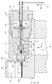
- With reference to FIG. 4, in which the same elements as in FIG. 3 are indicated by the same symbols, there is noted the metal package 11' with the
rectangular niche 12 and theside hole 15. Theniche 12 houses aMIC 16 and in thehole 15 is introduced a power supply connector CNT. - Between the
niche 12 and thehole 15 is included aresonant cavity 17 open at the bottom corresponding with the rectangular window F. Awave guide 18 with rectangular cross section is rigidly connected to the lower face of the package 11' and communicates with theresonant cavity 17 through the rectangular window F. - In the cross section shown in the figures it can be seen that the
resonant cavity 17 extends upward for nearly the entire thickness of the module. A cross section of the module along a plane perpendicular to that of the figure would show that the dimensions of said cavity in this plane coincide with those of the window F and therefore with those of a cross section of thewave guide 18. Thehole 15 is in communication with theresonant cavity 17 and allows introduction of everything needed to realise the transition. Thecavity 17 does not however remain open at the sides because, as seen below, the opening communicating with thehole 15 will be appropriately closed. - In the metal wall dividing the
rectangular niche 12 from theresonant cavity 17 is made ahole 19 in which is inserted acoaxial microline 20 of known type, e.g. that manufactured by Wiltron and indicated as a type K100 'glass support bead'. Themicroline 20 possesses acentral conductor 21 whose ends penetrate inside theniche 12 and thecavity 17 respectively. Therefore, and due to the fact that the dielectric of themicroline 20 is aglass cylinder 22, the latter is called also 'glass bead'. Ametallization 23 extending to the side surface of thedielectric cylinder 22 is the external coaxial conductor of themicroline 20. The ends of thecentral conductor 21 are welded to a microstrip of theMIC 16 connected to the electrodes of aGaAsFET 24 and to ametal probe 25 inside theresonant cavity 17 respectively. Themetallization 23 is welded to the package 11'. - The
probe 25 is a single cylindrical body made up of three parts having different diameters. Afirst part 25 placed between the other two and of greater diameter than the fatter, is the actual probe. A second part 25', of intermediate diameter, has a hole in which is introduced and welded thecentral conductor 21 of themicroline 20. Finally, athird part 25", of smaller diameter than the above, is a cylindrical conductor of diameter 0.2mm extending to approximately 3/4 the depth of thehole 15. - In the
resonant cavity 17 is introduced aprotective Teflon cap 26 comprising a smaller diameter extension 26' extending for part of thehole 15. Thecap 26 has acentral passing hole 27 in which it receives theprobe 25 complete with itsparts 25' and 25". Thehole 27 is restricted opposite theconductor 25". - In the
hole 15 is screwed a threadedcoaxial metal support 28 having a passingcentral hole 29 consisting of two adjoining sections of different diameter. After screwing in, thecoaxial support 28 nearly completely closes the opening of theresonant cavity 17 communicating with thehole 15. Theresonant cavity 17 now communicates with the exterior only through thehole 29. - Inside the smaller
diameter hole section 29 is visible the extension 26' of theTeflon cap 26 with in its centre thecylindrical conductor 25". The latter emerges from the Teflon to extend inside thehole section 29 of greater diameter where it traverses the centre of a discoid capacitor housed there. A first armature of thecapacitor 30 is in electric contact with the cylindrical conductor 25'' and with the power supply connector CNT. The latter is cylindrical and has acentral hole 31 in which is introduced and welded therein thecylindrical conductor 25". A second armature of thecapacitor 30 is in contact with thecoaxial metal support 28 at the point where thehole 29 changes diameter. - The end of the connector CNT in contact with the first armature of the
capacitor 30 has a diameter slightly greater than that of the remaining cylindrical body to aid the electrical contact. An insulatingplug 32 drilled in the centre closes thehole 29 hermetically. Anelectrical wire 33 welded to the power supply connector CNT connects the latter to a pole of a battery, not visible in the figures, which supplies the direct voltage DC1 adapted to the polarization of theGaAsFET 24 and the required current. The other pole of the battery is connected to the metal package 11' which constitutes the common reference ground for the module circuits. - As regards the seal of the module, it may be noted that the
microline 20 hermetically closes thehole 19. A similar closing takes place provided by an identical microline (not shown in the figures) located on the opposite side of theMIC 16. The two microlines together with acover 34 welded to acornice 35, in turn welded to the walls of theniche 12, seal hermetically theMIC 16 in said niche. - From all the above considerations, and as may be seen in FIG. 4, the transition which is the object of the present invention is made up of predominantly cylindrical elements connected together so as to be aligned along a common longitudinal symmetry axis. The latter coincides with the symmetry axis of the
coaxial microline 20,probe 25,discoid capacitor 30, power supply connector CNT,coaxial support 28 and also theTeflon cap 26 and theholes MIC 16 is parallel to said longitudinal symmetry axis which is perpendicular to the window F and consequently to the cross section of thewave guide 18 at the connection point thereof with themodule 11. - In operation, the transition of FIG. 4 couples the radio frequency signal RFin to the input electrode of the
GaAsFET 24 allowing voltage and current polarization to said transistor. More precisely, the direct current necessary for operation of theMIC 16 runs through theelectric wire 33, power supply connector CNT, cylindrical conductor 25',probe 25 and in its extension 25',central connector 21 of thecoaxial microline 20, and lastly the microstrip of theMIC 16, reaching the drain electrode of theGaAsFET 24. The above elements are all in electrical contact with each other and subjected to the same voltage DC1 applied between the source and drain electrodes of theGaAsFET 24, polarizing it. - The radio frequency signal RFin, carried by the
wave guide 18, is electromagnetically coupled with theresonant cavity 17 which resonates at the working frequency of 20GHz. Theprobe 25, which acts as an antenna inside thecavity 17, takes the signal RFin and transfers it to thecoaxial microline 20. Thence it runs through the microstrip of theMIC 16 and reaches the source electrode of theGaAsFET 24. The way to the power supply connector CNT is closed to the RFin signal by a decoupling filter consisting of the cylindrical conductor 25'' together with thediscoid capacitor 30. - The filtering configuration is that of FIG. 2 in which the inductor L corresponds to the section of the cylindrical conductor 25'' lying between the
probe 25 and thecapacitor 30. The capacitor C is thecapacitor 30. The port P1 corresponds to the connecting point of the conductor 25'' with theprobe 25, and lastly the port P2 is the connecting point of thewire 33 to the power supply connector CNT. - The electrical length of the section of conductor 25'' lying between the
probe 25 and the first armature of thecapacitor 30 is one-fourth the wave length of the RFin at the operating frequency of 20GHz. As is known, 'electrical length' is a number expressing the phase displacement introduced by a transmission line. Its expression is found by multiplying the phase constant β of the line by thephysical length 1 thereof. The constant β depends on the speed of propagation of the signal along the line. It should be stated that the speed of propagation of the signal travelling along the conductor 25'' changes in correspondence of the Teflon extension 26'. Indeed, it constitutes the entire insulating core of a coaxial line whose central conductor is 25'' and the coaxial conductor is the metal wall of the smaller diameter section of thehole 29. Calculation of the physical length of the one-fourth wave section consisting of the conductor 25'' allows for an average propagation speed. - The above section has high impedance at the signal RFin, obstructing passage of the signal currents to the connector CNT. In addition, because of its very small diameter and peculiar location in the
cavity 17, it does not disturb the cavity at all. - The
discoid capacitor 30 behaves like an ideal short circuit for the signal RFin, discharging to ground the residual signal current which traverses theconductor section 25". Theprobe 25, as concerns the signal RFin, is perfectly decoupled from the power supply connector CNT. Indeed, the short circuit represented by thecapacitor 30 is reported by theconductor section 25", one-fourth wave long, as an open circuit at the connection point with the probe. - The
probe 25 is dimensioned so as to maximize energy transfer, in the useful band of the radio frequency signal RFin, from theresonant cavity 17 to thecoaxial microline 20. The dimensions of the probe depend on the centre band frequency and the overall geometry of the transition. A study of the field radiated inside theresonant cavity 17 carried out by means of the Green functions provides a first solution of the problem. Theoretical considerations useful for this purpose are set forth, for example, in the volume entitled 'Microwave Transition Design', by J. Izadian, published by Artech House in 1988; or 'Field Theory of Guided Waves', by R. Collin, published by McGraw-Hill in 1960. - Measurements of the insertion losses performed between the input and the output of a circuit configuration comprising a guide-microstrip transition placed in series with a microstrip-guide transition, supplied an attenuation of only 0.2dB at 20GHz.
- Measurements of the frequency response of said circuit configuration, showed a flat response in an entire frequency interval extended beyond the limits of fo ±10%, where fo is the central frequency of 20GHz.
- Measurements of the return losses of the same configuration, supplied a value lower than -17dB in the entire above frequency interval.
- Significant tests were also performed on the individual amplifiers of the
module 11 and no instability was found. - All of the measurements performed show further significant advantages of the guide-microstrip transition described, and in particular: low losses, broad operating band, and excellent impedance matching.
Claims (9)
- Guide-microstrip transition in active modules (11) operating at microwaves and comprising a coaxial microline (20) which, while maintaining seal of the module, electromagnetically couples a microstrip of an active thin film circuit (16) placed inside a module niche (12) to a probe (25) acting as an antenna inside a resonant cavity (17) communicating with a three-dimensional wave guide carrying a radio-frequency signal, characterized in that:said probe (25) comprises a cylindrical conductor of small diameter (25") placed mainly in the resonant cavity (17) and connected to a first armature of a discoid capacitor (30) outside the resonant cavity;in that a power supply connector (CNT), connected to a pole of a battery having its other pole grounded, is also connected to said first armature of the discoid capacitor (30), a second armature of the capacitor being connected to ground;in that said coaxial microline (20), said cylindrical conductor (25"), said discoid capacitor (30) and said power supply connector (CNT) are aligned along a same longitudinal symmetry axis; andin that a section of said cylindrical conductor (25") lying between the probe (25) and the first armature of the discoid capacitor (30) has an electrical length equal to one-fourth the wavelength at the centre-band frequency of said radio frequency signal (RFin,RFout), said section having high impedance to said signal and constituting together with the discoid capacitor (30) a polarization filter for an active device (24) connected to said microstrip.
- Guide-microstrip transition in accordance with claim 1 characterized in that it also comprises a coaxial metal support (28) integral with the module and aligned along said longitudinal symmetry axis and having a first passing central hole (29) communicating with the outside of the module and with an aperture of said resonant cavity (17) from which emerges said cylindrical conductor (25"), said first hole (29) receiving also said discoid capacitor (30) and said power supply connector (CNT).
- Guide-microstrip transition in accordance with claim 2, characterized in that:said first hole (29) comprises two contiguous sections of different diameter in which a section of smaller diameter communicates with said resonant cavity (17) and houses said cylindrical conductor (25") and a section of larger diameter communicates with the outside of the module and houses said discoid capacitor (30) and said power supply connector (CNT),said second armature of the capacitor (30) is in contact with said coaxial metal support (28) at the point where said first hole (29) changes diameter, andsaid cylindrical conductor passes through a second central hole of said capacitor (30) penetrating into a third central hole (31) of said power supply connector (CNT).
- Guide-microstrip transition in accordance with claim 1 or 3, characterized in that said resonant cavity (17) includes a probe protective cap of dielectric material (26) comprising an extension (26') extending inside the section of smaller diameter of said first hole (29) and said protective cap (26,26') having a fourth central hole (27) in which is located said probe (25) including said cylindrical conductor (25").
- Active multiple module (11) operating at microwaves, characterized in that it comprises:2N first holes (15) made along two opposing side faces of the module and said holes terminating within first apertures of respective 2N opposing resonant cavities (17) having second apertures communicating with 2N wave guides (18) carrying radio frequency input and output signals (RFin,RFout) connected to one face of the module perpendicular to said side faces,N niches (12,13,14) housing as many N circuits active with microwaves in planar technology (16) and each niche lying between two of said opposing resonant cavities,2N coaxial microlines (20) which, maintaining the seal of the module, electromagnetically couple 2N microstrips of said N active circuits (16) to as many 2N probes (25) acting as antennas inside said 2N resonant cavities (17) and each probe (25) comprising in addition a cylindrical conductor of small diameter (25') emerging from the first aperture of the respective resonant cavity (17),2N discoid capacitors (30) located within said 2N first holes (15) outside the resonant cavities (17) and having first armatures connected to said cylindrical conductors (25") and second armatures connected to ground,2N power supply connectors (CNT) placed inside said first holes (15) outside the resonant cavities (17) which are also connected to said first armatures of the discoid capacitors (30) and also connected to a pole of a battery having its other pole grounded,said multiple module being further characterized in that the sections of said cylindrical conductors (25") lying between the probes (25) and said first armatures of the discoid capacitors (30) have an electrical length one-fourth the wave length at the centre-band frequency of the respective radio frequency signals (RFin,RFout), and said sections having high impedance to said signals and constituting together with the respective discoid capacitors (30) as many polarization filters for active devices (24) connected to said microstrips.
- Active multiple module in accordance with claim 5, characterized in that it also comprises 2N coaxial metal supports (28) inserted in said 2N first holes (15) and integral with the module and having along their axis respective second holes (29) communicating with the outside of the module and with said 2N first apertures of said 2N resonant cavities (17) from which emerge said cylindrical conductors (25"), said 2N second holes (29) receiving also said 2N discoid capacitors (30) and said 2N power supply connectors (CNT).
- Active multiple module in accordance with claim 6, characterized in that:said 2N second holes (29) comprise two respective contiguous sections of different diameter of which 2N sections of smaller diameter communicate with said 2N resonant cavities (17) and house said 2N cylindrical conductors (25"), and 2N sections of larger diameter communicate with the outside of the module and house said 2N discoid capacitors (30) and said 2N power supply connectors (CNT),said second armatures of the capacitors (30) are in contact with said coaxial metal supports (28) at the points where said second holes (29) change diameter, andsaid cylindrical conductors (25") pass through respective third holes made in the centre of said discoid capacitors (30), penetrating into respective fourth holes (31) made along the axis of said power supply connectors (CNT).
- Active multiple module in accordance with claim 5 or 7, characterized in that said 2N resonant cavities (17) include 2N respective probe protective caps of dielectric material (26) comprising as many extensions (26') extending inside the sections of smaller diameter of said second holes (29) and said protective caps (26,26') having along their axis respective fifth holes (27) inside which are housed said probes (25) including their cylindrical conductors (25'').
- Multiple active module in accordance with claim 5, characterized in that it is a multiple amplification module in which said N active circuits (16) are N identical amplifiers to whose inputs arrive N identical low power level radio frequency signals and at whose outputs are present N identical amplified signals reaching N wave guides which are part of a wave guide power combiner.
Applications Claiming Priority (2)
| Application Number | Priority Date | Filing Date | Title |
|---|---|---|---|
| ITMI920913A IT1254860B (en) | 1992-04-15 | 1992-04-15 | GUIDE-MICROSTRIP TRANSITION INTEGRATING A POLARIZATION FILTER IN HIGH PACKAGING HERMETIC ACTIVE MODULES, AND RELATED MODULES. |
| ITMI920913 | 1992-04-15 |
Publications (3)
| Publication Number | Publication Date |
|---|---|
| EP0565943A2 EP0565943A2 (en) | 1993-10-20 |
| EP0565943A3 EP0565943A3 (en) | 1994-08-03 |
| EP0565943B1 true EP0565943B1 (en) | 1997-10-15 |
Family
ID=11362944
Family Applications (1)
| Application Number | Title | Priority Date | Filing Date |
|---|---|---|---|
| EP93105295A Expired - Lifetime EP0565943B1 (en) | 1992-04-15 | 1993-03-30 | Guide-microstrip transition integrating a polarization filter in hermetic active modules with high packing and associated modules |
Country Status (5)
| Country | Link |
|---|---|
| EP (1) | EP0565943B1 (en) |
| DE (1) | DE69314525T2 (en) |
| ES (1) | ES2108154T3 (en) |
| GR (1) | GR3025327T3 (en) |
| IT (1) | IT1254860B (en) |
Families Citing this family (2)
| Publication number | Priority date | Publication date | Assignee | Title |
|---|---|---|---|---|
| US5495217A (en) * | 1994-06-30 | 1996-02-27 | Philips Electronics North America Corporation | Compact hybrid microwave choke |
| US7053643B2 (en) * | 2004-03-25 | 2006-05-30 | Intel Corporation | Radio frequency (RF) test probe |
Family Cites Families (4)
| Publication number | Priority date | Publication date | Assignee | Title |
|---|---|---|---|---|
| FR956487A (en) * | 1950-02-02 | |||
| GB1190496A (en) * | 1968-08-21 | 1970-05-06 | Marconi Co Ltd | Improvements in or relating to Waveguide to Coaxial Transitions. |
| US4152666A (en) * | 1977-08-01 | 1979-05-01 | Nippon Electric Co., Ltd. | FET Amplifier comprising a circulator for an input signal as an isolator |
| JPS61234601A (en) * | 1985-04-10 | 1986-10-18 | Nec Corp | Microwave circuit |
-
1992
- 1992-04-15 IT ITMI920913A patent/IT1254860B/en active IP Right Grant
-
1993
- 1993-03-30 EP EP93105295A patent/EP0565943B1/en not_active Expired - Lifetime
- 1993-03-30 ES ES93105295T patent/ES2108154T3/en not_active Expired - Lifetime
- 1993-03-30 DE DE69314525T patent/DE69314525T2/en not_active Expired - Fee Related
-
1997
- 1997-11-07 GR GR970402969T patent/GR3025327T3/en unknown
Also Published As
| Publication number | Publication date |
|---|---|
| IT1254860B (en) | 1995-10-11 |
| ITMI920913A1 (en) | 1993-10-15 |
| ITMI920913A0 (en) | 1992-04-15 |
| DE69314525D1 (en) | 1997-11-20 |
| ES2108154T3 (en) | 1997-12-16 |
| EP0565943A2 (en) | 1993-10-20 |
| GR3025327T3 (en) | 1998-02-27 |
| EP0565943A3 (en) | 1994-08-03 |
| DE69314525T2 (en) | 1998-03-19 |
Similar Documents
| Publication | Publication Date | Title |
|---|---|---|
| FI104661B (en) | Surface mounting filter with fixed transmission line connection | |
| Uchida et al. | Dual-band-rejection filter for distortion reduction in RF transmitters | |
| US7199680B2 (en) | RF module using mode converting structure having short-circuiting waveguides and connecting windows | |
| US4291278A (en) | Planar microwave integrated circuit power combiner | |
| US6313797B1 (en) | Dielectric antenna including filter, dielectric antenna including duplexer, and radio apparatus | |
| US5198786A (en) | Waveguide transition circuit | |
| EP1732158A1 (en) | Microwave filter including an end-wall coupled coaxial resonator | |
| US6396363B1 (en) | Planar transmission line to waveguide transition for a microwave signal | |
| CN109120302B (en) | Miniaturized ku frequency channel ODU module | |
| CN111063975A (en) | Ka-band GYSEL power divider based on ridge gap waveguide | |
| US5726664A (en) | End launched microstrip or stripline to waveguide transition with cavity backed slot fed by T-shaped microstrip line or stripline usable in a missile | |
| CN107275738B (en) | Waveguide-microstrip power combiner based on magnetic coupling principle | |
| US5724049A (en) | End launched microstrip or stripline to waveguide transition with cavity backed slot fed by offset microstrip line usable in a missile | |
| US20100045406A1 (en) | Rf filter module | |
| EP0565943B1 (en) | Guide-microstrip transition integrating a polarization filter in hermetic active modules with high packing and associated modules | |
| US4590617A (en) | Hermetically sealed planar structure for high frequency device | |
| US10804863B2 (en) | System and method for amplifying and combining radiofrequency power | |
| JPH0257363B2 (en) | ||
| CN112290171B (en) | Connecting device for coaxial cable and strip line, assembling method thereof and high frequency equipment | |
| CN109921163B (en) | Ka full-band power synthesis amplifier module and waveguide path structure thereof | |
| JP4167187B2 (en) | filter | |
| US6078221A (en) | Field effect transistor amplifier | |
| Duc et al. | A design of wideband high-power 3-dB quadrature coupler using defected ground structure for status data transmitting system | |
| Chen et al. | Synthesis and design of substrate integrated waveguide filter using predistortion technique | |
| CN115395191A (en) | Wide-stopband substrate integrated waveguide filter based on hybrid coupling |
Legal Events
| Date | Code | Title | Description |
|---|---|---|---|
| PUAI | Public reference made under article 153(3) epc to a published international application that has entered the european phase |
Free format text: ORIGINAL CODE: 0009012 |
|
| AK | Designated contracting states |
Kind code of ref document: A2 Designated state(s): DE ES FR GB GR IT NL SE |
|
| PUAL | Search report despatched |
Free format text: ORIGINAL CODE: 0009013 |
|
| AK | Designated contracting states |
Kind code of ref document: A3 Designated state(s): DE ES FR GB GR IT NL SE |
|
| 17P | Request for examination filed |
Effective date: 19950124 |
|
| RAP1 | Party data changed (applicant data changed or rights of an application transferred) |
Owner name: ITALTEL S.P.A. |
|
| GRAG | Despatch of communication of intention to grant |
Free format text: ORIGINAL CODE: EPIDOS AGRA |
|
| 17Q | First examination report despatched |
Effective date: 19970124 |
|
| GRAH | Despatch of communication of intention to grant a patent |
Free format text: ORIGINAL CODE: EPIDOS IGRA |
|
| GRAH | Despatch of communication of intention to grant a patent |
Free format text: ORIGINAL CODE: EPIDOS IGRA |
|
| GRAA | (expected) grant |
Free format text: ORIGINAL CODE: 0009210 |
|
| AK | Designated contracting states |
Kind code of ref document: B1 Designated state(s): DE ES FR GB GR IT NL SE |
|
| PG25 | Lapsed in a contracting state [announced via postgrant information from national office to epo] |
Ref country code: IT Free format text: LAPSE BECAUSE OF FAILURE TO SUBMIT A TRANSLATION OF THE DESCRIPTION OR TO PAY THE FEE WITHIN THE PRE;WARNING: LAPSES OF ITALIAN PATENTS WITH EFFECTIVE DATE BEFORE 2007 MAY HAVE OCCURRED AT ANY TIME BEFORE 2007. THE CORRECT EFFECTIVE DATE MAY BE DIFFERENT FROM THE ONE RECORDED.SCRIBED TIME-LIMIT Effective date: 19971015 Ref country code: GR Free format text: LAPSE BECAUSE OF FAILURE TO SUBMIT A TRANSLATION OF THE DESCRIPTION OR TO PAY THE FEE WITHIN THE PRESCRIBED TIME-LIMIT Effective date: 19971015 |
|
| REF | Corresponds to: |
Ref document number: 69314525 Country of ref document: DE Date of ref document: 19971120 |
|
| ET | Fr: translation filed | ||
| REG | Reference to a national code |
Ref country code: ES Ref legal event code: FG2A Ref document number: 2108154 Country of ref document: ES Kind code of ref document: T3 |
|
| REG | Reference to a national code |
Ref country code: GR Ref legal event code: FG4A Free format text: 3025327 |
|
| PG25 | Lapsed in a contracting state [announced via postgrant information from national office to epo] |
Ref country code: GB Free format text: LAPSE BECAUSE OF NON-PAYMENT OF DUE FEES Effective date: 19980330 |
|
| PG25 | Lapsed in a contracting state [announced via postgrant information from national office to epo] |
Ref country code: SE Free format text: LAPSE BECAUSE OF NON-PAYMENT OF DUE FEES Effective date: 19980331 Ref country code: ES Free format text: LAPSE BECAUSE OF EXPIRATION OF PROTECTION Effective date: 19980331 |
|
| PLBE | No opposition filed within time limit |
Free format text: ORIGINAL CODE: 0009261 |
|
| STAA | Information on the status of an ep patent application or granted ep patent |
Free format text: STATUS: NO OPPOSITION FILED WITHIN TIME LIMIT |
|
| PG25 | Lapsed in a contracting state [announced via postgrant information from national office to epo] |
Ref country code: NL Free format text: LAPSE BECAUSE OF NON-PAYMENT OF DUE FEES Effective date: 19981001 |
|
| 26N | No opposition filed | ||
| GBPC | Gb: european patent ceased through non-payment of renewal fee |
Effective date: 19980330 |
|
| NLV4 | Nl: lapsed or anulled due to non-payment of the annual fee |
Effective date: 19981001 |
|
| EUG | Se: european patent has lapsed |
Ref document number: 93105295.5 |
|
| REG | Reference to a national code |
Ref country code: ES Ref legal event code: FD2A Effective date: 20000601 |
|
| PGFP | Annual fee paid to national office [announced via postgrant information from national office to epo] |
Ref country code: DE Payment date: 20040517 Year of fee payment: 12 |
|
| PGFP | Annual fee paid to national office [announced via postgrant information from national office to epo] |
Ref country code: FR Payment date: 20050331 Year of fee payment: 13 |
|
| PG25 | Lapsed in a contracting state [announced via postgrant information from national office to epo] |
Ref country code: DE Free format text: LAPSE BECAUSE OF NON-PAYMENT OF DUE FEES Effective date: 20051001 |
|
| REG | Reference to a national code |
Ref country code: FR Ref legal event code: ST Effective date: 20061130 |
|
| PG25 | Lapsed in a contracting state [announced via postgrant information from national office to epo] |
Ref country code: FR Free format text: LAPSE BECAUSE OF NON-PAYMENT OF DUE FEES Effective date: 20060331 |