EP0564076B1 - Electrostatic discharge protection - Google Patents
Electrostatic discharge protection Download PDFInfo
- Publication number
- EP0564076B1 EP0564076B1 EP93300848A EP93300848A EP0564076B1 EP 0564076 B1 EP0564076 B1 EP 0564076B1 EP 93300848 A EP93300848 A EP 93300848A EP 93300848 A EP93300848 A EP 93300848A EP 0564076 B1 EP0564076 B1 EP 0564076B1
- Authority
- EP
- European Patent Office
- Prior art keywords
- internal circuit
- resistor
- conduction line
- input pad
- delay time
- Prior art date
- Legal status (The legal status is an assumption and is not a legal conclusion. Google has not performed a legal analysis and makes no representation as to the accuracy of the status listed.)
- Expired - Lifetime
Links
Images

Classifications
-
- H—ELECTRICITY
- H10—SEMICONDUCTOR DEVICES; ELECTRIC SOLID-STATE DEVICES NOT OTHERWISE PROVIDED FOR
- H10D—INORGANIC ELECTRIC SEMICONDUCTOR DEVICES
- H10D89/00—Aspects of integrated devices not covered by groups H10D84/00 - H10D88/00
- H10D89/60—Integrated devices comprising arrangements for electrical or thermal protection, e.g. protection circuits against electrostatic discharge [ESD]
- H10D89/601—Integrated devices comprising arrangements for electrical or thermal protection, e.g. protection circuits against electrostatic discharge [ESD] for devices having insulated gate electrodes, e.g. for IGFETs or IGBTs
-
- H—ELECTRICITY
- H10—SEMICONDUCTOR DEVICES; ELECTRIC SOLID-STATE DEVICES NOT OTHERWISE PROVIDED FOR
- H10D—INORGANIC ELECTRIC SEMICONDUCTOR DEVICES
- H10D89/00—Aspects of integrated devices not covered by groups H10D84/00 - H10D88/00
- H10D89/60—Integrated devices comprising arrangements for electrical or thermal protection, e.g. protection circuits against electrostatic discharge [ESD]
- H10D89/601—Integrated devices comprising arrangements for electrical or thermal protection, e.g. protection circuits against electrostatic discharge [ESD] for devices having insulated gate electrodes, e.g. for IGFETs or IGBTs
- H10D89/811—Integrated devices comprising arrangements for electrical or thermal protection, e.g. protection circuits against electrostatic discharge [ESD] for devices having insulated gate electrodes, e.g. for IGFETs or IGBTs using FETs as protective elements
- H10D89/819—Bias arrangements for gate electrodes of FETs, e.g. RC networks or voltage partitioning circuits
-
- H—ELECTRICITY
- H10—SEMICONDUCTOR DEVICES; ELECTRIC SOLID-STATE DEVICES NOT OTHERWISE PROVIDED FOR
- H10D—INORGANIC ELECTRIC SEMICONDUCTOR DEVICES
- H10D89/00—Aspects of integrated devices not covered by groups H10D84/00 - H10D88/00
- H10D89/60—Integrated devices comprising arrangements for electrical or thermal protection, e.g. protection circuits against electrostatic discharge [ESD]
- H10D89/601—Integrated devices comprising arrangements for electrical or thermal protection, e.g. protection circuits against electrostatic discharge [ESD] for devices having insulated gate electrodes, e.g. for IGFETs or IGBTs
- H10D89/911—Integrated devices comprising arrangements for electrical or thermal protection, e.g. protection circuits against electrostatic discharge [ESD] for devices having insulated gate electrodes, e.g. for IGFETs or IGBTs using passive elements as protective elements
Definitions
- the present invention relates to circuits for protecting an internal circuit of a semiconductor device from electrostatic discharge (ESD) phenomena.
- ESD electrostatic discharge
- a semiconductor memory device is typically provided with a circuit for protecting the internal circuit of a chip from static electricity which is applied from the exterior of the chip.
- the protection circuit includes an ESD prevention element which is provided in an input pad of the chip. That is, punch-through phenomena occur in the ESD prevention element in the input pad of the chip to bypass high voltage current caused by electrostatic discharge to ground voltage terminal when static electricity is applied from the exterior of the chip.
- the physical mechanism of ESD phenomena and preventive measures therefor are specifically described in "Internal Chip ESD Phenomena Protection Circuit" disclosed in IEEE TRANSACTION ON ELECTRON DEVICES, PP.2133-2139, Vol.35, No.12, Dec. 1989.
- our Patent Application GB 2 252 200 (corresponding to Korean Patent Application No.
- an input pad 1 and internal circuit 20 are connected by a metal line 10.
- a TFD element for preventing ESD and MOS diode T1 used for a clamping circuit are connected in parallel between the metal line 10 and ground voltage Vss.
- a resistor R1 consisting of an n + diffusion region between a node 11 connecting the metal line 10 with the TFD and a node 12 connecting the metal line 10 with the MOS diode T1.
- the resistor R1 has a high resistance value to protect a gate oxide layer 21 of an NMOS transistor N1 of the internal circuit 20 from an ESD stress voltage.
- a conventional circuit for protecting the internal circuit from electrostatic discharge results in a long RC delay time ⁇ 1 during the input signal transmission, which is caused by parasitic components induced between the node 12 and internal circuit 20, i.e. parasitic resistance r1 and capacitances c1 and c2.
- the RC delay time ⁇ 1 may be expressed by Eq. 1.
- the RC delay time ⁇ 1 becomes 2.4ns.
- the RC delay time increases with the values of the resistances and capacitances and the length of the metal line 10.
- the input signal transmission speed from the pad to the internal circuit is slowed down. Namely, an increase of the parametric values of the resistive components is needed to reduce the excessive ESD stress voltage, but this results in an excessive delay of the input signal transmission speed.
- Preferred embodiments of the present invention aim to provide a method of protecting an internal circuit of a semiconductor device from electrostatic discharge that may reduce the RC delay time of an input signal.
- said resistor is connected with a gate of a MOS transistor provided in said internal circuit.
- said resistor comprises a diffusion region with a conductive material.
- another resistor and clamping device are cascaded between said ground voltage terminal and a node on said conduction line connecting said input pad and RC delay stage.
- a metal line 100 connects an input pad 110 with an internal circuit 200.
- a TFD is connected between a node 101 and ground voltage Vss, and a resistor R2' and MOS diode T1 are cascaded between a node 102 and ground voltage Vss.
- the resistor R2' is employed to protect the MOS diode T1 used for a clamper circuit from an ESD stress voltage.
- the internal circuit 200 is, for example, an inverter which is generally employed in a CMOS integrated circuit.
- parasitic resistance r2 and capacitances c3 and c4 between the node 102 and internal circuit 200 of the metal line 100 .
- another resistor R2 is connected with an input terminal 210 of the internal circuit 200 in order to protect gate oxide layers of MOS transistors from the ESD stress voltage.
- the resistors R2' and R2 consist of n + diffusion regions.
- the resistor R2 for protecting the internal circuit 200 from the ESD stress voltage is connected between the RC delay stage which consists of the parasitic resistance r2 and capacitance c4 and the input terminal 210 of the internal circuit 200, so that the components which have a influence on the RC delay time are merely the parasitic resistance r2 and capacitance c4.
- the RC delay time ⁇ 2 may be expressed by Eq. 2.
- ⁇ 2 r2 ⁇ c4
- the values of the resistors R2' and R2 are set as 500 ⁇ . If the values of the resistors R2' and R2 are set more than 500 ⁇ in order to protect the gate oxide layer of the MOS transistor of the internal circuit 200 from greater ESD stress voltage, the RC delay time is not affected.
- the RC delay time is determined only by the parasitic resistance and capacitance which are physically inherent in the metal line 100 connecting the input pad 110 and internal circuit 200.
- the parasitic resistance will be in proportion to the length of the metal line 100.
- the resistor for protecting the internal circuit from electrostatic discharge is arranged so as not to affect the RC delay time, and the input signal delay time is considerably reduced by the inventive circuit for protecting the internal circuit from electrostatic discharge.
- ground potential (or like terms such as “ground voltage” or “earth” potential or voltage) is used conveniently in this specification to denote a reference potential.
- reference potential may typically be zero potential, it is not essential that it is so, and may be a reference potential other than zero.
Landscapes
- Semiconductor Integrated Circuits (AREA)
- Metal-Oxide And Bipolar Metal-Oxide Semiconductor Integrated Circuits (AREA)
Description
- The present invention relates to circuits for protecting an internal circuit of a semiconductor device from electrostatic discharge (ESD) phenomena.
- A semiconductor memory device is typically provided with a circuit for protecting the internal circuit of a chip from static electricity which is applied from the exterior of the chip. The protection circuit includes an ESD prevention element which is provided in an input pad of the chip. That is, punch-through phenomena occur in the ESD prevention element in the input pad of the chip to bypass high voltage current caused by electrostatic discharge to ground voltage terminal when static electricity is applied from the exterior of the chip. The physical mechanism of ESD phenomena and preventive measures therefor are specifically described in "Internal Chip ESD Phenomena Protection Circuit" disclosed in IEEE TRANSACTION ON ELECTRON DEVICES, PP.2133-2139, Vol.35, No.12, Dec. 1989. Also, our Patent Application GB 2 252 200 (corresponding to Korean Patent Application No. 91-1128) discloses means for preventing ESD between the input pad, source voltage and ground voltage, where an n+ diffusion region separated by a field oxide layer is connected with the pad and ground voltage so that current caused by static electricity is bypassed to the ground voltage terminal when static electricity or ESD stress voltage is applied to the pad, and the technique of which is fundamentally realized by the punch-through phenomena of the n+ diffusion region separated by the field oxide layer.
- Referring to Figure 1 of the accompanying diagrammatic drawings, which shows an equivalent circuit of a conventional circuit for protecting an internal circuit from electrostatic discharge, an
input pad 1 andinternal circuit 20 are connected by ametal line 10. A TFD element for preventing ESD and MOS diode T1 used for a clamping circuit are connected in parallel between themetal line 10 and ground voltage Vss. There is also provided a resistor R1 consisting of an n+ diffusion region between anode 11 connecting themetal line 10 with the TFD and anode 12 connecting themetal line 10 with the MOS diode T1. The resistor R1 has a high resistance value to protect agate oxide layer 21 of an NMOS transistor N1 of theinternal circuit 20 from an ESD stress voltage. When an ESD stress voltage is applied from theinput pad 1 to the metal line 10 (about 3000V is used as a test voltage), the excessive current is instantly discharged through TFD and the excessive voltage which is dropped through the resistor R1 is applied to theinternal circuit 20. Hence the ESD stress voltage is prevented from affecting theinternal circuit 20. - However, such a conventional circuit for protecting the internal circuit from electrostatic discharge results in a long RC delay time τ1 during the input signal transmission, which is caused by parasitic components induced between the
node 12 andinternal circuit 20, i.e. parasitic resistance r1 and capacitances c1 and c2. The RC delay time τ1 may be expressed by Eq. 1. - If it is assumed that R1, r1, c1 and c2 are respectively 500Ω, 200Ω, 2pF and 2pF, then the RC delay time τ1 becomes 2.4ns. The RC delay time increases with the values of the resistances and capacitances and the length of the
metal line 10. In addition, if the RC delay time increases, the input signal transmission speed from the pad to the internal circuit is slowed down. Namely, an increase of the parametric values of the resistive components is needed to reduce the excessive ESD stress voltage, but this results in an excessive delay of the input signal transmission speed. - Preferred embodiments of the present invention aim to provide a method of protecting an internal circuit of a semiconductor device from electrostatic discharge that may reduce the RC delay time of an input signal.
- According to one aspect of the present invention, there is provided a method of protecting an internal circuit of a semiconductor device from electrostatic discharge as defined in
claim 1. - Further modifications are defined in claims 2-5.
- Preferably, said resistor is connected with a gate of a MOS transistor provided in said internal circuit.
- Preferably, said resistor comprises a diffusion region with a conductive material.
- Preferably, another resistor and clamping device are cascaded between said ground voltage terminal and a node on said conduction line connecting said input pad and RC delay stage.
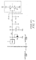
- For a better understanding of the invention, and to show how the same may be carried into effect, reference will now be made, by way of example, to Figure 2 of the accompanying diagrammatic drawings, which is an equivalent circuit of a circuit for protecting an internal circuit of a semiconductor device from electrostatic discharge.
- Referring to Figure 2, a
metal line 100 connects aninput pad 110 with aninternal circuit 200. A TFD is connected between anode 101 and ground voltage Vss, and a resistor R2' and MOS diode T1 are cascaded between anode 102 and ground voltage Vss. The resistor R2' is employed to protect the MOS diode T1 used for a clamper circuit from an ESD stress voltage. Theinternal circuit 200 is, for example, an inverter which is generally employed in a CMOS integrated circuit. There also exist parasitic resistance r2 and capacitances c3 and c4 between thenode 102 andinternal circuit 200 of themetal line 100 . In addition, another resistor R2 is connected with aninput terminal 210 of theinternal circuit 200 in order to protect gate oxide layers of MOS transistors from the ESD stress voltage. The resistors R2' and R2 consist of n+ diffusion regions. - The resistor R2 for protecting the
internal circuit 200 from the ESD stress voltage is connected between the RC delay stage which consists of the parasitic resistance r2 and capacitance c4 and theinput terminal 210 of theinternal circuit 200, so that the components which have a influence on the RC delay time are merely the parasitic resistance r2 and capacitance c4. Hence, the RC delay time τ2 may be expressed by Eq. 2. - If it is assumed that the values of the parasitic resistance r2 and capacitance c4 are 200Ω and 2pF respectively, then the RC delay time τ2 becomes 0.4ns, which is reduced by 2ns compared to the RC delay time τ1(=2.4ns) of the conventional circuit of Figure 1. In the present embodiment, the values of the resistors R2' and R2 are set as 500Ω. If the values of the resistors R2' and R2 are set more than 500Ω in order to protect the gate oxide layer of the MOS transistor of the
internal circuit 200 from greater ESD stress voltage, the RC delay time is not affected. Namely, according to this embodiment of the present invention, the RC delay time is determined only by the parasitic resistance and capacitance which are physically inherent in themetal line 100 connecting theinput pad 110 andinternal circuit 200. Of course, the parasitic resistance will be in proportion to the length of themetal line 100. - Thus the resistor for protecting the internal circuit from electrostatic discharge is arranged so as not to affect the RC delay time, and the input signal delay time is considerably reduced by the inventive circuit for protecting the internal circuit from electrostatic discharge.
- The term "ground potential" (or like terms such as "ground voltage" or "earth" potential or voltage) is used conveniently in this specification to denote a reference potential. As will be understood by those skilled in the art, although such reference potential may typically be zero potential, it is not essential that it is so, and may be a reference potential other than zero.
- The invention is not restricted to the details of the foregoing embodiment.
Claims (5)
- A method of protecting an internal circuit (200) of a semiconductor device from electrostatic discharge comprising:characterized by:connecting a first end of a conduction line (100) having between said first end and a second end an RC delay stage (r2, c4), directly to an input pad (110) for receiving an input signal to be applied to said internal circuit;connecting a punch-through element (TFD), for connecting said conduction line (100) with a ground voltage (Vss), directly to said conduction line between said input pad (110) and said RC delay stage (r2, c4);determining that the RC delay time (τ2) for the propagation of signals from the input pad to the second end of the conduction line when said second end of the conduction line is connected directly to said internal circuit (200) is the same as the RC delay time (τ2) for the propagation of signals from the input pad to the second end of the conduction line when respective ends of a resistor R2 having a particular resistance value are connected directly to said second end of said conduction line and said internal circuit (200); andsubsequently connecting respective ends of a resistor R2 having that particular resistance value directly to said second end of said conduction line and said internal circuit (200).
- A method as defined in Claim 1, wherein said resistor (R2) has a value of 500Ω, and the values of said parasitic resistance and capacitance are 200Ω and 2pF, respectively.
- A method as defined in Claim 1 or Claim 2, wherein said resistor (R2) is connected with a gate (210) of a MOS transistor provided in said internal circuit (200).
- A method as defined in Claim 3, wherein said resistor (R2) comprises a diffusion region with a conductive material.
- A method as defined in Claim 1, 2, 3 or 4, wherein another resistor (R2') and clamping device (T1) are cascaded between said ground voltage and a node (102) on said conduction line (100) connecting said input pad (110) and RC delay stage (r2, c3, c4).
Applications Claiming Priority (2)
| Application Number | Priority Date | Filing Date | Title |
|---|---|---|---|
| KR1019920005352A KR950007572B1 (en) | 1992-03-31 | 1992-03-31 | Esd protection circuit |
| KR535292 | 1992-03-31 |
Publications (2)
| Publication Number | Publication Date |
|---|---|
| EP0564076A1 EP0564076A1 (en) | 1993-10-06 |
| EP0564076B1 true EP0564076B1 (en) | 2002-05-22 |
Family
ID=19331165
Family Applications (1)
| Application Number | Title | Priority Date | Filing Date |
|---|---|---|---|
| EP93300848A Expired - Lifetime EP0564076B1 (en) | 1992-03-31 | 1993-02-04 | Electrostatic discharge protection |
Country Status (4)
| Country | Link |
|---|---|
| US (1) | US5430602A (en) |
| EP (1) | EP0564076B1 (en) |
| JP (1) | JPH05299574A (en) |
| KR (1) | KR950007572B1 (en) |
Families Citing this family (16)
| Publication number | Priority date | Publication date | Assignee | Title |
|---|---|---|---|---|
| US5852317A (en) * | 1995-03-31 | 1998-12-22 | National Semiconductor Corporation | Method to reduce gate oxide damage due to non-uniform plasmas in read only memory arrays |
| JPH11103021A (en) * | 1997-09-26 | 1999-04-13 | Seiko Instruments Inc | Protection circuit and electronic circuit using protection circuit |
| US6002567A (en) * | 1997-10-17 | 1999-12-14 | Lsi Logic Corporation | ESD protection for high voltage level input for analog application |
| US6725439B1 (en) | 1998-01-29 | 2004-04-20 | International Business Machines Corporation | Method of automated design and checking for ESD robustness |
| US6069782A (en) * | 1998-08-26 | 2000-05-30 | Integrated Device Technology, Inc. | ESD damage protection using a clamp circuit |
| US20020060343A1 (en) * | 1999-03-19 | 2002-05-23 | Robert J. Gauthier | Diffusion resistor/capacitor (drc) non-aligned mosfet structure |
| TW445627B (en) * | 1999-10-04 | 2001-07-11 | Winbond Electronics Corp | Electrostatic discharge buffer apparatus |
| US6400204B1 (en) * | 2000-07-26 | 2002-06-04 | Agere Systems Guardian Corp. | Input stage ESD protection for an integrated circuit |
| US6678133B2 (en) * | 2001-03-09 | 2004-01-13 | Micron Technology, Inc. | Electrostatic discharge protection with input impedance |
| JP3608199B2 (en) * | 2001-10-30 | 2005-01-05 | ローム株式会社 | IC interface system and IC |
| KR100482370B1 (en) * | 2002-09-27 | 2005-04-13 | 삼성전자주식회사 | Semiconductor device having difference thickness of gate oxide |
| EP1642370B1 (en) * | 2003-06-30 | 2009-09-23 | Nxp B.V. | Protection circuit for an integrated circuit device |
| DE602005012817D1 (en) * | 2004-09-30 | 2009-04-02 | Huawei Tech Co Ltd | PROCESS SYSTEM FOR REALIZING COMMUNICATION |
| US7453676B2 (en) * | 2005-11-16 | 2008-11-18 | Huh Yoon J | RC-triggered ESD power clamp circuit and method for providing ESD protection |
| US7760477B1 (en) * | 2006-10-06 | 2010-07-20 | Altera Corporation | CDM performance of high speed CLK inputs |
| US7978448B2 (en) * | 2007-08-20 | 2011-07-12 | Microchip Technology Incorporated | Hybrid circuit for circuit protection and switching |
Family Cites Families (10)
| Publication number | Priority date | Publication date | Assignee | Title |
|---|---|---|---|---|
| GB1209271A (en) * | 1967-02-27 | 1970-10-21 | Hitachi Ltd | Improvements in semiconductor devices |
| JPS57152160A (en) * | 1981-03-13 | 1982-09-20 | Mitsubishi Electric Corp | Protective circuit for input |
| DE3378807D1 (en) * | 1982-10-20 | 1989-02-02 | Philips Nv | Integrated circuit comprising an input protection device |
| US4745450A (en) * | 1984-03-02 | 1988-05-17 | Zilog, Inc. | Integrated circuit high voltage protection |
| JPH0691196B2 (en) * | 1984-07-25 | 1994-11-14 | 株式会社日立製作所 | Semiconductor device |
| JPS6271275A (en) * | 1985-09-25 | 1987-04-01 | Toshiba Corp | Semiconductor integrated circuit |
| JPH0616558B2 (en) * | 1987-01-28 | 1994-03-02 | 三菱電機株式会社 | Input protection device for semiconductor device |
| JPH0695545B2 (en) * | 1988-01-07 | 1994-11-24 | 株式会社東芝 | Semiconductor integrated circuit |
| JPH02294075A (en) * | 1989-05-08 | 1990-12-05 | Matsushita Electron Corp | Semiconductor protecting device |
| JP2626229B2 (en) * | 1989-10-12 | 1997-07-02 | 日本電気株式会社 | Semiconductor input protection device |
-
1992
- 1992-03-31 KR KR1019920005352A patent/KR950007572B1/en not_active Expired - Fee Related
-
1993
- 1993-01-29 JP JP5013897A patent/JPH05299574A/en active Pending
- 1993-02-04 EP EP93300848A patent/EP0564076B1/en not_active Expired - Lifetime
- 1993-03-31 US US08/041,224 patent/US5430602A/en not_active Expired - Lifetime
Also Published As
| Publication number | Publication date |
|---|---|
| KR930020660A (en) | 1993-10-20 |
| EP0564076A1 (en) | 1993-10-06 |
| US5430602A (en) | 1995-07-04 |
| KR950007572B1 (en) | 1995-07-12 |
| JPH05299574A (en) | 1993-11-12 |
Similar Documents
| Publication | Publication Date | Title |
|---|---|---|
| EP0564076A1 (en) | Electrostatic discharge protection | |
| US5880917A (en) | Well resistor for ESD protection of CMOS circuits | |
| US7224560B2 (en) | Destructive electrical transient protection | |
| US6507471B2 (en) | ESD protection devices | |
| US5901022A (en) | Charged device mode ESD protection circuit | |
| US4527213A (en) | Semiconductor integrated circuit device with circuits for protecting an input section against an external surge | |
| US6028465A (en) | ESD protection circuits | |
| US6873507B2 (en) | Electrostatic discharge protection with input impedance | |
| US4893159A (en) | Protected MOS transistor circuit | |
| US5521415A (en) | Semiconductor device having a circuit for protecting the device from electrostatic discharge | |
| US5535086A (en) | ESD protection circuit and method for BICMOS devices | |
| US4864454A (en) | Means for reducing damage to JFETs from electrostatic discharge events | |
| US4962320A (en) | Input protection circuit for MOS device | |
| US8014112B2 (en) | Integrated circuit with device for protection against electrostatic discharges | |
| KR100205099B1 (en) | Data output circuit of semiconductor memory device and output method thereof | |
| DE69331941T2 (en) | Protection against electrostatic discharge | |
| JPS6340373A (en) | Input protective circuit for semiconductor device | |
| KR100323452B1 (en) | Eletromagnetic Interference prevention circuit | |
| KR960002096B1 (en) | Semiconductor device having electrostatic discharge protection | |
| GB2220791A (en) | An input protection device for a semiconductor integrated circuit | |
| JPH03218678A (en) | Semiconductor integrated device | |
| JPS59207653A (en) | Input protecting circuit for mos transistor | |
| KR20000045471A (en) | Electrostatic discharge preventing circuit of semiconductor device |
Legal Events
| Date | Code | Title | Description |
|---|---|---|---|
| PUAI | Public reference made under article 153(3) epc to a published international application that has entered the european phase |
Free format text: ORIGINAL CODE: 0009012 |
|
| AK | Designated contracting states |
Kind code of ref document: A1 Designated state(s): DE FR GB IT |
|
| 17P | Request for examination filed |
Effective date: 19940315 |
|
| 17Q | First examination report despatched |
Effective date: 19960102 |
|
| GRAG | Despatch of communication of intention to grant |
Free format text: ORIGINAL CODE: EPIDOS AGRA |
|
| GRAG | Despatch of communication of intention to grant |
Free format text: ORIGINAL CODE: EPIDOS AGRA |
|
| GRAH | Despatch of communication of intention to grant a patent |
Free format text: ORIGINAL CODE: EPIDOS IGRA |
|
| GRAH | Despatch of communication of intention to grant a patent |
Free format text: ORIGINAL CODE: EPIDOS IGRA |
|
| GRAA | (expected) grant |
Free format text: ORIGINAL CODE: 0009210 |
|
| PG25 | Lapsed in a contracting state [announced via postgrant information from national office to epo] |
Ref country code: IT Free format text: LAPSE BECAUSE OF FAILURE TO SUBMIT A TRANSLATION OF THE DESCRIPTION OR TO PAY THE FEE WITHIN THE PRE;WARNING: LAPSES OF ITALIAN PATENTS WITH EFFECTIVE DATE BEFORE 2007 MAY HAVE OCCURRED AT ANY TIME BEFORE 2007. THE CORRECT EFFECTIVE DATE MAY BE DIFFERENT FROM THE ONE RECORDED.SCRIBED TIME-LIMIT Effective date: 20020522 Ref country code: FR Free format text: LAPSE BECAUSE OF FAILURE TO SUBMIT A TRANSLATION OF THE DESCRIPTION OR TO PAY THE FEE WITHIN THE PRESCRIBED TIME-LIMIT Effective date: 20020522 |
|
| REG | Reference to a national code |
Ref country code: GB Ref legal event code: FG4D |
|
| REF | Corresponds to: |
Ref document number: 69331941 Country of ref document: DE Date of ref document: 20020627 |
|
| EN | Fr: translation not filed | ||
| PLBE | No opposition filed within time limit |
Free format text: ORIGINAL CODE: 0009261 |
|
| 26N | No opposition filed |
Effective date: 20030225 |
|
| PGFP | Annual fee paid to national office [announced via postgrant information from national office to epo] |
Ref country code: DE Payment date: 20120123 Year of fee payment: 20 |
|
| PGFP | Annual fee paid to national office [announced via postgrant information from national office to epo] |
Ref country code: GB Payment date: 20120131 Year of fee payment: 20 |
|
| REG | Reference to a national code |
Ref country code: DE Ref legal event code: R071 Ref document number: 69331941 Country of ref document: DE |
|
| REG | Reference to a national code |
Ref country code: GB Ref legal event code: PE20 Expiry date: 20130203 |
|
| PG25 | Lapsed in a contracting state [announced via postgrant information from national office to epo] |
Ref country code: DE Free format text: LAPSE BECAUSE OF EXPIRATION OF PROTECTION Effective date: 20130205 Ref country code: GB Free format text: LAPSE BECAUSE OF EXPIRATION OF PROTECTION Effective date: 20130203 |