EP0562397B1 - Differentieller Diskriminator mit dualer Schwelle - Google Patents
Differentieller Diskriminator mit dualer Schwelle Download PDFInfo
- Publication number
- EP0562397B1 EP0562397B1 EP93104121A EP93104121A EP0562397B1 EP 0562397 B1 EP0562397 B1 EP 0562397B1 EP 93104121 A EP93104121 A EP 93104121A EP 93104121 A EP93104121 A EP 93104121A EP 0562397 B1 EP0562397 B1 EP 0562397B1
- Authority
- EP
- European Patent Office
- Prior art keywords
- control
- power controller
- threshold
- voltage
- thresholds
- Prior art date
- Legal status (The legal status is an assumption and is not a legal conclusion. Google has not performed a legal analysis and makes no representation as to the accuracy of the status listed.)
- Expired - Lifetime
Links
Images



Classifications
-
- H—ELECTRICITY
- H03—ELECTRONIC CIRCUITRY
- H03K—PULSE TECHNIQUE
- H03K17/00—Electronic switching or gating, i.e. not by contact-making and –breaking
- H03K17/16—Modifications for eliminating interference voltages or currents
- H03K17/161—Modifications for eliminating interference voltages or currents in field-effect transistor switches
-
- H—ELECTRICITY
- H03—ELECTRONIC CIRCUITRY
- H03K—PULSE TECHNIQUE
- H03K17/00—Electronic switching or gating, i.e. not by contact-making and –breaking
- H03K17/30—Modifications for providing a predetermined threshold before switching
- H03K17/302—Modifications for providing a predetermined threshold before switching in field-effect transistor switches
-
- H—ELECTRICITY
- H03—ELECTRONIC CIRCUITRY
- H03K—PULSE TECHNIQUE
- H03K17/00—Electronic switching or gating, i.e. not by contact-making and –breaking
- H03K17/51—Electronic switching or gating, i.e. not by contact-making and –breaking characterised by the components used
- H03K17/56—Electronic switching or gating, i.e. not by contact-making and –breaking characterised by the components used by the use, as active elements, of semiconductor devices
- H03K17/687—Electronic switching or gating, i.e. not by contact-making and –breaking characterised by the components used by the use, as active elements, of semiconductor devices the devices being field-effect transistors
Definitions
- the present invention relates to electronic power control devices and specifically to MOS-gated devices, such as MOSFET transistors and insulated gate bipolar transistors, that switch high voltages to motors and other loads in half-bridge and full-bridge multiphase configurations.
- MOS-gated devices such as MOSFET transistors and insulated gate bipolar transistors
- Digital logic is an almost ideal mechanism for switching power on and off to loads, especially with high-current, high-voltage MOSFET transistors that do the actual switching.
- loads such as motors and florescent lights operate at voltages substantially higher than the five volts direct current (DC) used by most digital logic.
- DC direct current
- Some form of level shifting is required to interface the MOSFET switch that floats at high-voltage and the digital logic that is ground referenced.
- Fig. 1 illustrates a half-bridge circuit 10 for driving a fluorescent light 12.
- a pair of MOSFET transistors 14 and 16 switch their junction between ground and a positive high-voltage potential (+HV).
- the lower end of light 12 is thus driven between ground and +HV through an impedance matching circuit comprising a capacitor 17 and an inductor 18.
- An oscillator 19 is connected to a low-side driver 20 which in turn controls the gate of transistor 16 and a high-side driver 22 that controls the gate of transistor 14.
- a logic supply voltage (Vdd) powers low-side driver 20 directly and high-side driver 22 indirectly with the help of a bootstrap diode 24 and a bootstrap capacitor 26.
- Low-side driver 20 controls high-side driver 22 through a pair of control lines 28 and 30.
- a comparator in high-side driver 22 will latch the switch transistor 14 on and off according to the relative voltages between lines 28 and 30.
- Fig. 2 illustrates the basic functional parts of low-side driver 20 which comprises a linear regulator 40, an inverter 42 with hysteresis, an under-voltage lockout 44, a buffer with hysteresis 46, a NAND-gate 48, a pulse circuit 50, a pair of transistors 52 and 54, and an output inverter driver 56 which controls the gate of transistor 16.
- An input 58 receives a control signal that is combined in NAND-gate 48 with an under-voltage signal from lockout 44. If the logic power Vdd falls below a predetermined threshold, driver 56 will be prevented from turning transistor 16 on.
- An input 60 receives an inverted control signal that will turn transistor 14 on and off by pulsing either transistor 52 or transistor 54 on and the other being off. Which line, 28 or 30, is lower than the other will be sensed by high-side driver 22 and used to ultimately control the gate of transistor 14.
- Fig. 3 illustrates high-side driver 22 which comprises a linear regulator 70, a discriminator 72, an under-voltage lockout 74, an AND-gate 76, a flip-flop 78, an output driver 80, a pair of constant current sources 82 and 84, a pair of transistors 86 and 88, a pair of Zener diodes 90 and 92, and a pair of input pull-up resistors 94 and 96.
- An output 98 is connected to driver 80 and the gate of transistor 14.
- a reference common 99 connects to the source of transistor 14 and can swing from below ground in circuit 10 to above +HV, in some cases. Diode 24 takes advantage of these swings to provide a supply voltage Vddh.
- Transistors 86 and 88 in a common source configuration present a high-impedance comparator input to control lines 28 and 30. If the voltage on line 30 is more negative than a predetermined threshold, e.g. Vddh-1.5 volts, and transistor 52 (Fig. 2) is off and transistor 54 is on, then the set (S) input of flip-flop 78 will go true, turning transistor 14 (Fig. 1) off. If the voltage on line 28 is more negative than the predetermined threshold, and transistor 54 (Fig. 2) is off and transistor 52 is on, then the reset (R) input of flip-flop 78 will go true, turning transistor 14 on. Table I summarizes the control function.
- a predetermined threshold e.g. Vddh-1.5 volts
- Noise on lines 28 and 30 can easily be induced and proper circuit 10 operation depends on a high degree of common mode noise rejection. If an imbalance develops between lines 28 and 30, such as can happen with unequal stray line capacitances and high frequency environments, false triggering of transistor 14 can occur. These false triggers can be very serious if they occur while transistor 16 is on, because +HV will momentarily find a short path to ground through transistor 14, causing a high current pulse.
- a high-side driver is needed that is immune to false triggering caused by rapid common mode slewing of the control lines.
- An improved threshold region of the comparators is needed to prevent a slight mismatching of the control lines to trigger an unintended change of state.
- an embodiment of the present invention is a high-side driver comprising a pair of differential input controls each of which are coupled to a pair of comparators having first and second thresholds set at Vddh-1.5 volts and Vddh-2.5 volts, respectively.
- a logic block in front of a set-reset flip-flop recognizes only signals on the control lines where one is less than the Vddh-1.5 volt threshold and the other exceeds the Vddh-2.5 volt threshold. If signals on either or both of the control lines are between Vddh-1.5 volts and Vddh-2.5 volts, the logic block will prevent a change of state of the flip-flop which controls a high-voltage switch transistor connected to a load.
- the high-side driver further includes an under-voltage lockout to prevent false operation of the high-voltage switch transistor during the initial power up phase.
- An advantage of the present invention is that a high-side driver is provided that has an increased level of common mode rejection on the control inputs.
- Another advantage of the present invention is that a high-side driver is provided that substantially eliminates false triggering of the output by high-frequency and high-voltage switching of a load.
- Another advantage of the present invention is that a high-side driver is provided that is less sensitive to control line routing and device placement on a printed circuit board.
- Another advantage of the present invention is that a high-side driver can be implemented with a small number of circuit elements.
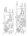
- an embodiment of the present invention is a high-side transistor driver 100 comprising a linear regulator 102, a four-input logic block 104, an under-voltage lockout 106, an AND-gate 108, a flip-flop 110, an output driver 112, a set of four constant current sources 114-117, a set of four transistors 118-121, a pair of Zener diodes 122 and 124, and a pair of input pull-up resistors 126 and 128.
- An output 130 couples driver 112 to the gate of an external high-voltage switch transistor (e.g., transistor 14 in Fig. 1).
- a reference 132 connects to the source of the external switch transistor.
- a pair of control input lines 134 and 136 receive a differential signal from a low side driver (e.g., low-side driver 20 in Fig. 1).
- Transistors 120 and 119 together with constant current sources 116 and 115, form a 1.5 volt comparator function for inputs "A1" and "B1" of logic block 104, respectively.
- Input "A1” will be true whenever the voltage on line 134 drops more than 1.5 volts more negative than Vddh, which serves as a reference.
- Input "A2” will be true whenever the voltage on line 134 drops more than 2.5 volts more negative than Vddh.
- Input "B1” will be true whenever the voltage on line 136 drops more than 1.5 volts more negative than Vddh.
- Input "B2” will be true whenever the voltage on line 136 drops more than 2.5 volts more negative than Vddh.
- Logic block 104 is such that it recognizes only signals on the control lines 134 and 136 where one is less than the Vddh-1.5 volt threshold and the other exceeds the Vddh-2.5 volt threshold. If signals on either or both of the control lines 134 and 136 are between Vddh-1.5 volts and Vddh-2.5 volts, or both are less negative than Vddh-1.5 volts or both are more negative than Vddh-2.5 volts, logic block 104 will prevent a change of state of flip-flop 110.
- Table II summarizes the logic states that result for various combinations of input voltages (X) on line 134 and input voltages (Y) on line 136. These voltages are negative, with respect to Vddh.
- the set, reset and output of flip-flop 110 are "S”, “R” and “Q”, respectively. It is assumed in Table II that an under-voltage condition does not exist, so "R” is received only from logic block 104.
- the asterisk in the first two columns of Table II is meant to call attention to the fact that voltage threshold one (V T1 ) represents Vddh-1.5 volts and voltage threshold two (V T2 ) represents Vddh-2.5 volts.
- a second embodiment of the present invention is illustrated in Fig. 5.
- a dual-threshold discriminator 150 is functionally equivalent to high-side driver 100, except that a linear regulator and under-voltage detector are not included. These functions can be provided externally.
- Discriminator 150 comprises a plurality of input protection Zener diodes 152, a pair of clamping diodes 154 and 155 with a pair of dropping resistors 156 and 157, a pair of series input resistors 158, a set of four comparison transistors 160-163, a set of four constant current sources 164-167, a set of four logic protection Zener diodes 168-171, a logic block 172, a flip-flop 174, a NAND-gate 176, and a pair of output inverters 178 and 180.
- Logic block 172 includes a plurality of inverters 182, an AND-gate 184 and a NAND-gate 186.
- Flip-flop 174 is constructed of a pair of NOR-gates 188 and 190.
- a dual-input control signal is received on a pair of lines 192 and 194 and an output line 196 controls the gate of an external high-side, high-voltage switch transistor that has its source connected to a common 197.
- An under-voltage control signal is received on an input 198.
- Power (Vddh) to operate discriminator 150 is supplied to a terminal 199.
- transistors 160-163 can be the same size and the current through constant-current sources 164-167 can be individually adjusted to set the two thresholds.
- a still further alternative is to use voltage taps on resistors 156 and 157, as shown in Fig. 6, for a discriminator 150' which is similar to discriminator 150.
- the gate of transistor 163 has a tap on resistor 157.
- the gate of transistor 161 is similarly tapped on resistor 156.
- Transistors 161 and 163 with constant current sources 165 and 167 form the 1.5 volt threshold comparator.
- circuitry between lines 134 and 136 and driver 112 could be replaced by an OP-amplifier configured to accept differential voltage inputs and that has a small amount of the output signal feedback to the noninverting terminal.
- a differential hysteresis effect is created in which a difference of voltage on control lines 134 and 136 must exceed some minimum set by the amount of positive feedback in order for the output to switch state.
- linear circuits could also be used in a configuration that compares the control lines 134 and 136 independently to the two thresholds.
- the current state-of-the-art is such that such linear circuits are limited in their frequency ranges and add a level of complexity that increases the costs of manufacturing.
- the limitations of such configurations may improve with future developments in those areas.
Landscapes
- Electronic Switches (AREA)
- Power Conversion In General (AREA)
- Circuit Arrangements For Discharge Lamps (AREA)
Claims (10)
- Leistungsregler (100, 150) mit folgenden Merkmalen:erste (134, 192) und zweite (136, 194) Steuerleitungen zur Signalisierung, ob ein potentialseitig höher angeschlossener, mit einer Last (12) verbundener Hochspannungsschalttransistor (14) ein- oder ausgeschaltet werden sollte;ein erster Vergleicher (115, 116, 119, 120, 165, 167, 161, 163), der einen ersten Schwellwert aufweist und mit der ersten (134) und der zweiten (136) Steuerleitung verbunden ist;gekennzeichnet durch einen zweiten Vergleicher (114, 117, 118, 121, 160, 162, 164, 166), der einen zweiten Schwellwert aufweist und mit der ersten (134, 192) und der zweiten (136, 194) Steuerleitung verbunden ist, wobei der zweite Schwellwert im wesentlichen unterschiedlich von dem ersten Schwellwert ist;erste logische Einrichtungen (104, 172, 182, 184, 186), um den höher spannungsseitig angeordneten Hochspannungsschalttransistor (14) einzuschalten, wenn ein Signal auf der ersten (134, 192) Steuerleitung sowohl den ersten als auch den zweiten Schwellwert übersteigt und ein Signal auf der zweiten (136, 194) Steuerleitung unterhalb sowohl des ersten als auch des zweiten Schwellwertes liegt; undzweite logische Einrichtungen (104, 172, 182, 184, 186), um den höher spannungsseitig angeordneten Hochspannungsschalttransistor (14) auszuschalten, wenn ein Signal auf der ersten Steuerleitung (134, 192) unterhalb sowohl des ersten wie des zweiten Schwellwertes ist und ein Signal auf der zweiten Steuerleitung (136, 194) sowohl den ersten und den zweiten Schwellwert übersteigt.
- Leistungsregler nach Anspruch 1, dadurch gekennzeichnet, daß der erste Schwellwert in dem ersten Vergleicher (115, 116, 119, 120, 161, 163, 165, 167) ungefähr 1,5 Volt beträgt.
- Leistungsregler nach Anspruch 1 oder 2, dadurch gekennzeichnet, daß der zweite Schwellwert in dem zweiten Vergleicher (114, 117, 118, 121, 160, 162, 164, 166) ungefähr 2,5 Volt beträgt.
- Leistungsregler nach Anspruch 1, 2 oder 3, dadurch gekennzeichnet, daß die ersten und zweiten logischen Einrichtungen jeweils ein Nand-Glied umfassen, welches jeweilige Verbindungen zu den Setz- und Rücksetzeingängen eines Flip-Flops (110) aufweist.
- Leistungsregler nach Anspruch 4, dadurch gekennzeichnet, daß das Flip-Flop (110) einen Ausgang aufweist, der einen Puffertreiber (112) zur Steuerung des Gates des Hochspannungsschalttransistors (14) steuert.
- Leistungsregler nach einem der Ansprüche 1-5, dadurch gekennzeichnet, daß mindestens zwei Zener-Dioden (122, 124, 152) mit jeweils der ersten (134, 192) und der zweiten (136, 194) Steuerleitung verbunden sind, um die Spannungsausschläge des auf der ersten (134, 192) und der zweiten (136, 194) Steuerleitung empfangenen Signals zu begrenzen.
- Leistungsregler nach einem der Ansprüche 1-6, dadurch gekennzeichnet, daß der erste und zweite Vergleicher eine Mehrzahl von Transistoren (160-163, 118-121) und Konstantstromquellen (164-167, 114-117) umfassen und jeweilige Schwellwerte aufweisen, die durch die relative physikalische Größe dieser Transistoren bestimmt werden.
- Leistungsregler nach einem der Ansprüche 1-6, dadurch gekennzeichnet, daß der erste und zweite Vergleicher eine Mehrzahl von Transistoren (160-163, 118-121) und Konstantstromquellen (164-167, 114-117) umfassen und jeweilige Schwellwerte aufweisen, die durch die Konstantstromquellen bestimmt werden, welche auf unterschiedliche Pegel eingestellt sind.
- Leistungsregler nach einem der Ansprüche 1-6, dadurch gekennzeichnet, daß der erste und zweite Vergleicher zwei Vorwiderstände (156, 157) zur Herabsetzung ankommender Steuersignale und eine Mehrzahl von Transistoren (160-163) und Konstantstromquellen (164-167) umfassen und jeweilige Schwellwerte aufweisen, die durch die Abzapfungen an den Vorwiderständen (156, 157) bestimmt werden.
- Leistungsregler nach einem der Ansprüche 4-9, der potentialseitig höher angeschlossene Transistortreiber zur Regelung von Hochspannungslasten in Vollbrücken- oder Halbbrückenschaltung konfiguriert ist, dadurch gekennzeichnet, daß die erste (134, 192) und die zweite (136, 194) Steuerleitung Eingangsleitungen zur Führung von Steuersignalen ausgebildet sind, die anzeigen, ob eine Last (12) ein- oder auszuschalten ist;daß ferner ein Operationsverstärker vorgesehen ist, der eine erste Hystereseeinrichtung zur Konditionierung der Steuersignale auf der ersten Steuereingangsleitung (134, 192) darstellt, so daß ein ankommendes Analogsignal in ein abgehendes Digitalsignal umgewandelt wird, wobei die Hysterese so definiert wird, daß das analoge Eingangssignal mindestens zwei vorbestimmte analoge Werte durchqueren muß, bevor das digitale Ausgangssignal seinen Zustand ändert;daß eine zweite Hystereseeinrichtung zur Konditionierung des Steuersignals auf der zweiten Steuereingangsleitung (136, 194) dient, so daß ein ankommendes Analogsignal in ein abgehendes Digitalsignal umgewandelt wird, wobei die Hysterese so definiert ist, daß das analoge Eingangssignal mindestens durch zwei vorbestimmte analoge Werte hindurchgehen muß, bevor das digitale Ausgangssignal seinen Zustand ändert,um so den Betrieb des Komparators und der logischen Einrichtung zu erfüllen,und daß das digitale Flip-Flop (110, 174) die jeweiligen digitalen Ausgangssignale der ersten und der zweiten Hytereseeinrichtung empfängt und ein Ausgangssignal aufweist, um den potentialseitig höher angeschlossenen Transistor (14) in Vollwegbrückenschaltung undHalbbrückenschaltung (10) für die Hochspannungslast (12) zu steuern.
Applications Claiming Priority (2)
| Application Number | Priority Date | Filing Date | Title |
|---|---|---|---|
| US07/856,550 US5274274A (en) | 1992-03-23 | 1992-03-23 | Dual threshold differential discriminator |
| US856550 | 1992-03-23 |
Publications (3)
| Publication Number | Publication Date |
|---|---|
| EP0562397A2 EP0562397A2 (de) | 1993-09-29 |
| EP0562397A3 EP0562397A3 (en) | 1993-10-27 |
| EP0562397B1 true EP0562397B1 (de) | 1997-07-02 |
Family
ID=25323919
Family Applications (1)
| Application Number | Title | Priority Date | Filing Date |
|---|---|---|---|
| EP93104121A Expired - Lifetime EP0562397B1 (de) | 1992-03-23 | 1993-03-13 | Differentieller Diskriminator mit dualer Schwelle |
Country Status (4)
| Country | Link |
|---|---|
| US (1) | US5274274A (de) |
| EP (1) | EP0562397B1 (de) |
| JP (1) | JP3217181B2 (de) |
| DE (1) | DE69311823T2 (de) |
Families Citing this family (28)
| Publication number | Priority date | Publication date | Assignee | Title |
|---|---|---|---|---|
| US5545955A (en) * | 1994-03-04 | 1996-08-13 | International Rectifier Corporation | MOS gate driver for ballast circuits |
| US5543740A (en) * | 1995-04-10 | 1996-08-06 | Philips Electronics North America Corporation | Integrated half-bridge driver circuit |
| US5502412A (en) * | 1995-05-04 | 1996-03-26 | International Rectifier Corporation | Method and circuit for driving power transistors in a half bridge configuration from control signals referenced to any potential between the line voltage and the line voltage return and integrated circuit incorporating the circuit |
| US6172383B1 (en) | 1997-12-31 | 2001-01-09 | Siliconix Incorporated | Power MOSFET having voltage-clamped gate |
| US6268242B1 (en) | 1997-12-31 | 2001-07-31 | Richard K. Williams | Method of forming vertical mosfet device having voltage clamped gate and self-aligned contact |
| DE19827705C1 (de) | 1998-06-22 | 1999-10-28 | Siemens Ag | Resetschaltung |
| DE10200917A1 (de) * | 2002-01-12 | 2003-07-24 | Philips Intellectual Property | Treiberschaltung zur Steuerung eines resonanten Konverters |
| WO2007003967A2 (en) * | 2005-07-06 | 2007-01-11 | Cambridge Semiconductor Limited | Switch mode power supply control systems |
| US7710098B2 (en) * | 2005-12-16 | 2010-05-04 | Cambridge Semiconductor Limited | Power supply driver circuit |
| GB2433363A (en) * | 2005-12-16 | 2007-06-20 | Cambridge Semiconductor Ltd | A high side transistor drive circuit |
| GB0615029D0 (en) * | 2005-12-22 | 2006-09-06 | Cambridge Semiconductor Ltd | Switch mode power supply controllers |
| US7733098B2 (en) * | 2005-12-22 | 2010-06-08 | Cambridge Semiconductor Limited | Saturation detection circuits |
| US7242149B1 (en) * | 2006-08-09 | 2007-07-10 | Cheng-Lung Ku | Lamp driving circuit with floating power supply driver |
| US7518885B2 (en) | 2006-10-04 | 2009-04-14 | Power Integrations, Inc. | Method and apparatus for a control circuit with multiple operation modes |
| US7576528B2 (en) | 2006-10-04 | 2009-08-18 | Power Integrations, Inc. | Control circuit responsive to an impedance |
| US7502236B2 (en) * | 2006-10-04 | 2009-03-10 | Power Integrations, Inc. | Power supply controller responsive to a feedforward signal |
| US8796884B2 (en) * | 2008-12-20 | 2014-08-05 | Solarbridge Technologies, Inc. | Energy conversion systems with power control |
| US9263895B2 (en) | 2007-12-21 | 2016-02-16 | Sunpower Corporation | Distributed energy conversion systems |
| JP5475970B2 (ja) * | 2008-08-05 | 2014-04-16 | 株式会社日立製作所 | レベルシフト回路、スイッチング素子駆動回路及びインバータ装置 |
| US20100157632A1 (en) * | 2008-12-20 | 2010-06-24 | Azuray Technologies, Inc. | Energy Conversion Systems With Power Control |
| US8570075B2 (en) * | 2011-12-29 | 2013-10-29 | Nxp B.V. | Gate driver with digital ground |
| DE102014203064A1 (de) * | 2014-02-20 | 2015-08-20 | Robert Bosch Gmbh | Pegelumsetzer und Verfahren zur Pegelumsetzung |
| US9537338B2 (en) | 2014-09-16 | 2017-01-03 | Navitas Semiconductor Inc. | Level shift and inverter circuits for GaN devices |
| US9571093B2 (en) | 2014-09-16 | 2017-02-14 | Navitas Semiconductor, Inc. | Half bridge driver circuits |
| US9831867B1 (en) | 2016-02-22 | 2017-11-28 | Navitas Semiconductor, Inc. | Half bridge driver circuits |
| US10381821B2 (en) * | 2016-09-26 | 2019-08-13 | Infineon Technologies Ag | Power switch device |
| US10008942B1 (en) | 2017-04-12 | 2018-06-26 | Power Integrations, Inc. | High side signal interface in a power converter |
| TWI641225B (zh) * | 2018-05-03 | 2018-11-11 | 廣達電腦股份有限公司 | 電壓帶通致能電路 |
Family Cites Families (6)
| Publication number | Priority date | Publication date | Assignee | Title |
|---|---|---|---|---|
| IT1228028B (it) * | 1988-12-15 | 1991-05-27 | Sgs Thomson Microelectronics | Generatore di segnali di pilotaggio per transistori connessi in configurazione a semiponte |
| US4950913A (en) * | 1989-04-21 | 1990-08-21 | Kephart David A | Programmable timer power switch unit |
| US4989127A (en) * | 1989-05-09 | 1991-01-29 | North American Philips Corporation | Driver for high voltage half-bridge circuits |
| JPH03169273A (ja) * | 1989-11-22 | 1991-07-22 | Mitsubishi Electric Corp | スイッチングデバイス駆動回路 |
| FR2656965B1 (fr) * | 1990-01-09 | 1995-01-20 | Sgs Thomson Microelectronics | Commande et controle d'un commutateur de puissance. |
| US5206540A (en) * | 1991-05-09 | 1993-04-27 | Unitrode Corporation | Transformer isolated drive circuit |
-
1992
- 1992-03-23 US US07/856,550 patent/US5274274A/en not_active Expired - Lifetime
-
1993
- 1993-03-13 DE DE69311823T patent/DE69311823T2/de not_active Expired - Lifetime
- 1993-03-13 EP EP93104121A patent/EP0562397B1/de not_active Expired - Lifetime
- 1993-03-22 JP JP06206693A patent/JP3217181B2/ja not_active Expired - Lifetime
Also Published As
| Publication number | Publication date |
|---|---|
| EP0562397A2 (de) | 1993-09-29 |
| JP3217181B2 (ja) | 2001-10-09 |
| JPH0645898A (ja) | 1994-02-18 |
| US5274274A (en) | 1993-12-28 |
| EP0562397A3 (en) | 1993-10-27 |
| DE69311823D1 (de) | 1997-08-07 |
| DE69311823T2 (de) | 1998-01-29 |
Similar Documents
| Publication | Publication Date | Title |
|---|---|---|
| EP0562397A2 (de) | Differentieller Diskriminator mit dualer Schwelle | |
| EP0409328B1 (de) | Geschaltete Brückenanordnung | |
| US7345521B2 (en) | High frequency switch circuit | |
| JP3037760B2 (ja) | ハーフブリッジ駆動装置 | |
| US20080211547A1 (en) | Inverter citcuit | |
| US20020014900A1 (en) | Power device driving circuit and associated methods | |
| US5256882A (en) | Signal transmission circuit having a latch-up function | |
| US4970620A (en) | FET bridge protection circuit | |
| US4883984A (en) | PIN diode switch | |
| US4647794A (en) | Solid state relay having non overlapping switch closures | |
| WO1993000744A1 (en) | A 0-100 % duty cycle, transformer isolated fet driver | |
| US7119497B2 (en) | Dimmer for resistive or capacitive loads | |
| EP2979519B1 (de) | Schaltung und verfahren zur unabhängigen steuerung von seriell verbundenen leds | |
| WO1988005228A1 (en) | Ttl compatible cmos input circuit | |
| US4712020A (en) | Bias control circuit for RF switch | |
| WO2003081777A1 (en) | Optoelectronic receiver circuit for digital communication | |
| EP0399333A2 (de) | ECL/CML-Schaltung mit Emitterfolger-Stromschaltern | |
| US5027020A (en) | Zero voltage switching AC relay circuit | |
| US20020057114A1 (en) | Circuit for driving gate of IGBT inverter | |
| US6847175B2 (en) | Lighting ballast with reverse current flow protection | |
| US6421260B1 (en) | Shutdown circuit for a half-bridge converter | |
| EP0447989B1 (de) | Treiberschaltung hoher Geschwindigkeit für MOSFET-Transistoren | |
| US7070102B2 (en) | Dual light source voltage-modulated reciprocal control circuit for scanner | |
| US5204550A (en) | Output stage having reduced current consumption | |
| US6420804B1 (en) | Circuit for switching direction of current |
Legal Events
| Date | Code | Title | Description |
|---|---|---|---|
| PUAI | Public reference made under article 153(3) epc to a published international application that has entered the european phase |
Free format text: ORIGINAL CODE: 0009012 |
|
| PUAL | Search report despatched |
Free format text: ORIGINAL CODE: 0009013 |
|
| AK | Designated contracting states |
Kind code of ref document: A2 Designated state(s): DE FR GB IT NL SE |
|
| AK | Designated contracting states |
Kind code of ref document: A3 Designated state(s): DE FR GB IT NL SE |
|
| 17P | Request for examination filed |
Effective date: 19940406 |
|
| 17Q | First examination report despatched |
Effective date: 19950704 |
|
| GRAG | Despatch of communication of intention to grant |
Free format text: ORIGINAL CODE: EPIDOS AGRA |
|
| GRAH | Despatch of communication of intention to grant a patent |
Free format text: ORIGINAL CODE: EPIDOS IGRA |
|
| ITF | It: translation for a ep patent filed | ||
| GRAH | Despatch of communication of intention to grant a patent |
Free format text: ORIGINAL CODE: EPIDOS IGRA |
|
| GRAA | (expected) grant |
Free format text: ORIGINAL CODE: 0009210 |
|
| AK | Designated contracting states |
Kind code of ref document: B1 Designated state(s): DE FR GB IT NL SE |
|
| REF | Corresponds to: |
Ref document number: 69311823 Country of ref document: DE Date of ref document: 19970807 |
|
| ET | Fr: translation filed | ||
| PLBE | No opposition filed within time limit |
Free format text: ORIGINAL CODE: 0009261 |
|
| 26N | No opposition filed | ||
| REG | Reference to a national code |
Ref country code: GB Ref legal event code: IF02 |
|
| PGFP | Annual fee paid to national office [announced via postgrant information from national office to epo] |
Ref country code: FR Payment date: 20120406 Year of fee payment: 20 |
|
| PGFP | Annual fee paid to national office [announced via postgrant information from national office to epo] |
Ref country code: GB Payment date: 20120326 Year of fee payment: 20 Ref country code: SE Payment date: 20120328 Year of fee payment: 20 Ref country code: IT Payment date: 20120327 Year of fee payment: 20 |
|
| PGFP | Annual fee paid to national office [announced via postgrant information from national office to epo] |
Ref country code: DE Payment date: 20120328 Year of fee payment: 20 Ref country code: NL Payment date: 20120329 Year of fee payment: 20 |
|
| REG | Reference to a national code |
Ref country code: DE Ref legal event code: R071 Ref document number: 69311823 Country of ref document: DE |
|
| REG | Reference to a national code |
Ref country code: DE Ref legal event code: R071 Ref document number: 69311823 Country of ref document: DE |
|
| REG | Reference to a national code |
Ref country code: NL Ref legal event code: V4 Effective date: 20130313 |
|
| REG | Reference to a national code |
Ref country code: GB Ref legal event code: PE20 Expiry date: 20130312 |
|
| PG25 | Lapsed in a contracting state [announced via postgrant information from national office to epo] |
Ref country code: GB Free format text: LAPSE BECAUSE OF EXPIRATION OF PROTECTION Effective date: 20130312 Ref country code: DE Free format text: LAPSE BECAUSE OF EXPIRATION OF PROTECTION Effective date: 20130314 |
|
| REG | Reference to a national code |
Ref country code: SE Ref legal event code: EUG |