EP0561580A2 - Ladungsträger-Durchflusskontrollanordnung - Google Patents
Ladungsträger-Durchflusskontrollanordnung Download PDFInfo
- Publication number
- EP0561580A2 EP0561580A2 EP93301928A EP93301928A EP0561580A2 EP 0561580 A2 EP0561580 A2 EP 0561580A2 EP 93301928 A EP93301928 A EP 93301928A EP 93301928 A EP93301928 A EP 93301928A EP 0561580 A2 EP0561580 A2 EP 0561580A2
- Authority
- EP
- European Patent Office
- Prior art keywords
- storage region
- regions
- charge
- region
- charge carrier
- Prior art date
- Legal status (The legal status is an assumption and is not a legal conclusion. Google has not performed a legal analysis and makes no representation as to the accuracy of the status listed.)
- Granted
Links
Images


Classifications
-
- B—PERFORMING OPERATIONS; TRANSPORTING
- B82—NANOTECHNOLOGY
- B82Y—SPECIFIC USES OR APPLICATIONS OF NANOSTRUCTURES; MEASUREMENT OR ANALYSIS OF NANOSTRUCTURES; MANUFACTURE OR TREATMENT OF NANOSTRUCTURES
- B82Y10/00—Nanotechnology for information processing, storage or transmission, e.g. quantum computing or single electron logic
-
- H—ELECTRICITY
- H10—SEMICONDUCTOR DEVICES; ELECTRIC SOLID-STATE DEVICES NOT OTHERWISE PROVIDED FOR
- H10D—INORGANIC ELECTRIC SEMICONDUCTOR DEVICES
- H10D30/00—Field-effect transistors [FET]
- H10D30/01—Manufacture or treatment
- H10D30/014—Manufacture or treatment of FETs having zero-dimensional [0D] or one-dimensional [1D] channels, e.g. quantum wire FETs, single-electron transistors [SET] or Coulomb blockade transistors
-
- H—ELECTRICITY
- H10—SEMICONDUCTOR DEVICES; ELECTRIC SOLID-STATE DEVICES NOT OTHERWISE PROVIDED FOR
- H10D—INORGANIC ELECTRIC SEMICONDUCTOR DEVICES
- H10D30/00—Field-effect transistors [FET]
- H10D30/40—FETs having zero-dimensional [0D], one-dimensional [1D] or two-dimensional [2D] charge carrier gas channels
- H10D30/402—Single electron transistors; Coulomb blockade transistors
-
- H—ELECTRICITY
- H10—SEMICONDUCTOR DEVICES; ELECTRIC SOLID-STATE DEVICES NOT OTHERWISE PROVIDED FOR
- H10D—INORGANIC ELECTRIC SEMICONDUCTOR DEVICES
- H10D62/00—Semiconductor bodies, or regions thereof, of devices having potential barriers
- H10D62/80—Semiconductor bodies, or regions thereof, of devices having potential barriers characterised by the materials
- H10D62/85—Semiconductor bodies, or regions thereof, of devices having potential barriers characterised by the materials being Group III-V materials, e.g. GaAs
Definitions
- This invention relates to a charge carrier flow control device which may be used to provide a current standard.
- Odintsov supra has proposed a device in which the flow of current is controlled by a combination of two adjustable tunnelling barriers and the effect of Coulomb blockade.
- the device in effect operates as a turnstile so as to allow the passage of electrons in synchronism with an applied radio frequency signal.
- a similar device is disclosed by Kouwenhoven, L.P., Johnson, A.T., Van der Vaart, N.C. and Harmans, C.J.P.M., Appl. Phys Lett., 67 1626 (1991). The basic operation of the prior device will now be described with reference to Figures 1 and 2.
- the device consists of a semi-conductor including a GaAs/GaAlAs heterojunction that provides a two dimensional electron gas.
- An overlaid pattern of electrodes 1, 2, 3 receives control potentials so as to establish an essentially two dimensional quantum dot 4 in the two dimensional electron gas.
- the electrodes 1, 2 each cooperate with the electrode 3 to define tunnelling barrier regions 5, 6 on either side of the dot.
- the region 7 to the left of the dot 4 is considered to be a source of electrons and the region 8 is considered to be a drain
- individual electrons from source 7 tunnel through the barrier 5 into the dot 4 and thereafter tunnel from the dot 4 through barrier 6 to the drain 8.
- the tunnelling is controlled by a rf signal applied to the electrodes 1, 2.
- FIG. 2 shows the potential barriers developed in use of the device.
- this shows the equilibrium situation in which the potential barriers 5, 6 are of equal height.
- the energy state ⁇ (N) of the quantum dot 4 is below the Fermi level for the source and drain regions 7, 8.
- the barriers 5, 6 each have a very small capacitance then if an electron tunnels from the source 7 through the barrier 5 into the dot 4, the energy of the dot is raised by the Coulomb energy of the electron.
- This is represented in Figure 2b and the increased energy level in the dot 4 is represented by ⁇ (N+1) and is effectively the original Fermi energy shifted upward by the electrostatic charging energy.
- This increased energy level ⁇ (N+1) is greater than the energy of electrons from the source and so no further electrons can enter the dot 4 from the source 7.
- Coulomb blockade only a single electron can enter the dot 4 from the source.
- the level ⁇ (N+1) should lie between Fermi energies of the source and drain regions as shown in Figure 2b. This condition can be achieved by moving the Fermi level in the quantum dot 4 by way of an extra gate (not shown) on the surface of the device.
- the lefthand barrier 5 is lowered. Under such conditions, a single electron from the source will tunnel into the central region of the dot 4, raising the energy of the dot from the Nth energy level to the (N+1)th energy level marked by the solid line. Further electron tunnelling into the dot 4 from the source is prevented by Coulomb blockade. In this respect, the next available energy state (N+2) in the dot 4 is above the Fermi level in the source, and as a result no electrons can enter the (N+2) level. It will be appreciated that the temperature of the system tends to 0°K so electrons do not achieve energies that reach the (N+2) energy level in the dot.
- the electron will stay in the level (N+1) as it is unable to tunnel in either direction due to the size of the left and right hand barriers 5, 6.
- the right hand barrier 6 is lowered permitting the electron to tunnel out through the lowered barrier into the drain region 8.
- an external sinusoidal signal to the tunnel barriers such that their heights are modulated 180° out of phase.
- electrons pass through the device in the manner of a turnstile at a rate determined by the frequency of the externally applied signal.
- the current produced by a single gate of this type is extremely small and in order to provide a measurable current standard, it has been proposed to connect a plurality of such gates in parallel.
- a charge carrier flow control device comprising: a substrate including a region of high charge carrier mobility that defines a charge storage region; means defining first and second potential barrier regions bounding the storage region; means for selectively raising and lowering the probability of charge carriers passing through the barrier regions, the arrangement being such that charge carrier passage into the storage region is limited by Coulomb blockade whereby a discrete level of charge flows into and out of the storage region in response to the selective raising and lowering of said probability characterised by the substrate having been selectively subjected to fabrication processing that at least partially destroys said high charge carrier mobility except in one area whereby said area defines said charge storage region.
- a charge storage region is produced in a two dimensional electron gas, by confining the gas to a particular region using focussed ion beam (FIB) techniques.
- FIB focussed ion beam
- the two dimensional electron gas 13 is constrained to a small region defining an elongate wire structure by the implantation of ions into the AlGaAs layer 11 using an FIB.
- the beam strength is selected so that sufficient numbers of ions are injected into the crystal so as to neutralise the donor impurities 12 in the AlGaAs layer 11 with the result that the two dimensional electron gas at the heterojunction ceases to exist in the ion-doped regions.
- a resist pattern is applied to the surface of the wafer.
- a PMMA resist is applied to the surface and then a pattern is written into the resist using electron beam lithography techniques.
- gate patterns are applied in order to create tunnel barriers at opposite ends of the wire.
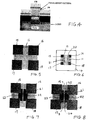
- the process step for the fabrication of the device will now be described in more detail with reference to Figures 5 to 8.
- a GaAs/GaAlAs heterojunction is formed on a substrate so as to define a two dimensional electron gas in the manner shown in section in Figure 3. Fabrication of such a junction is well known in the art and will not be described in detail herein.
- the two dimensional electron gas is formed in a cruciform configuration with four desposited metal gate regions 15, 16, 17, 18 being formed therein.
- the layer of PMMA resist is spun onto the surface of the substrate and two windows 19, 20 are opened in the resist using an electron beam.
- a thin line of resist 21 is left on the substrate between the opening 19, 20 in order to define an elongate wire in the two dimensional electron gas 13 as will be explained hereinafter.
- the substrate is thereafter subjected to FIB exposure, typically with a source of gallium ions, which produces implantation in the AlGaAs layer 11 in regions 22, 23 corresponding to the windows 19, 20.
- No implantation occurs in the region 21 due to the shielding effect of the PMMA resin.
- the regions 15-18 are unaffected by the FIB implantation as they are shielded by metal surface gates.
- an essentially two dimensional electron wire structure is formed beneath the region 21 in the two dimensional electron gas.
- the effect of the gallium ion implantation is to destroy the two dimensional electron gas in the regions 22, 23 so that the wire is in effect surrounded by regions of very low conductivity, so as to define the wire, without the need for external applied fields as in the prior art.
- tunnelling barriers are formed at opposite ends of the wire 21 by means of electrode regions 24, 25 which extend transversely across the wire and are connected to gate regions 15, 18 respectively.
- the electrode regions 24, 25 are typically written onto the surface of the substrate by electron beam techniques.
- the region 7 of the two dimensional electron gas can be considered as the source of the device, the region 8 can be considered the drain and the region 21 of the wire between the tunnelling barriers 24, 25 can be considered as a charge storage region.
- a metalisation overlayer can be applied to the gate regions 15 - 18 to form appropriate contacts.
- the region 15 defines a contact TB1 for the tunnelling barrier 25, and region 16 forms an isolation contact to shepherd the carriers through the central channel, 21.
- Region 17 provides a means of connecting the control gate 26, whereby the Schottky gate 26, which overlays the channel region produces a means of "tuning" the energy levels of the charge storage region, 21 to the correct level for operation of the device.
- the FIB implanted regions 22, 23 are arranged to define a pattern of FIB implantation that provides re-entrant regions 27, 28 which constitute in-plane gates connected to the 2-DEG gas 29, 30 that surrounds the wire 21.
- the electron gas regions 29, 30 are coupled to independent contacts (not shown) which allow the application of an external bias to the central/channel region 21 of the wire.
- the resulting structure is effectively a transistor which operates by manipulating the flow of single electrons.
- rf signals 180° out of phase are applied to the electrodes TB1, TB2 so as to raise and lower cyclicly the tunnelling barriers produced by electrode regions 24, 25.
- the device operates in a manner analogous to that described with reference to Figure 2.
- the barrier defined by the electrode 25 is momentarily reduced, a single electron can tunnel through the barrier into the wire 21.
- the energy levels are so arranged that only a single electron can tunnel into the region 21. Further electron tunnelling is inhibited by Coulomb blockade, i.e. the energy level of the next state permissible in the region 21 is greater than the tunnelling energy of a second electron so that the second electron cannot enter the region 21 when the barrier potential of region 25 is lowered.
- the height of the tunnelling barrier associated with electrode 24 is momentarily lowered and as a result a single electron tunnels through the barrier into the drain 8.
- the FIB implants 22, 23 may exhibit p- or n-type characteristics so that the gate 26 may make an electrical connection with the regions 22, 23 that would cause the channel in wire 21 to be widened or narrowed depending on the polarity of the applied voltage. Similar comments apply in relation to gates 15 - 18. In order to prevent this, it may be necessary to include an insulating layer (not shown) between the gates and the FIB implants.
- FIG 11 An alternative embodiment, which avoids the need for such an insulating layer, is shown in Figure 11.
- the heterostructure shown in Figure 3 is provided with a PMMA resist pattern 14 in the manner described with reference to Figure 4 and then is subject to a shallow mesa etch so as to remove the donors from the AlGaAs layer 11 except in the region protected by the PMMA resist pattern 14, thereby destroying the 2-DEG except in the region which is to define the wire 21.
- the main effect of geometrical inaccuracies in the wire and gate sizes will result in a spread in the essentially quantised magnitude of charging energy.
- the associated charging energy is of the order of 6°K (expressed as a termpature). It can be shown that if the gates are fabricated with tolerances of 10-20%, the error in the charging energy is approximately in the same range (approximately 15-30%) leading to a fluctuation in charging energy across the whole array of around 1K.
- the device can count single electrons which would enable a standard electric current to be established which is referenced to a standard of frequency i.e. the frequency applied to the tunnel barriers TB1, 2.
Landscapes
- Engineering & Computer Science (AREA)
- Chemical & Material Sciences (AREA)
- Nanotechnology (AREA)
- Physics & Mathematics (AREA)
- Mathematical Physics (AREA)
- Theoretical Computer Science (AREA)
- Crystallography & Structural Chemistry (AREA)
- Junction Field-Effect Transistors (AREA)
- Insulated Gate Type Field-Effect Transistor (AREA)
Applications Claiming Priority (2)
| Application Number | Priority Date | Filing Date | Title |
|---|---|---|---|
| GB9206149 | 1992-03-19 | ||
| GB929206149A GB9206149D0 (en) | 1992-03-19 | 1992-03-19 | Charge carrier flow control device |
Publications (3)
| Publication Number | Publication Date |
|---|---|
| EP0561580A2 true EP0561580A2 (de) | 1993-09-22 |
| EP0561580A3 EP0561580A3 (en) | 1994-07-06 |
| EP0561580B1 EP0561580B1 (de) | 2001-08-08 |
Family
ID=10712550
Family Applications (1)
| Application Number | Title | Priority Date | Filing Date |
|---|---|---|---|
| EP93301928A Expired - Lifetime EP0561580B1 (de) | 1992-03-19 | 1993-03-15 | Ladungsträger-Durchflusskontrollanordnung |
Country Status (3)
| Country | Link |
|---|---|
| EP (1) | EP0561580B1 (de) |
| DE (1) | DE69330535T2 (de) |
| GB (1) | GB9206149D0 (de) |
Cited By (2)
| Publication number | Priority date | Publication date | Assignee | Title |
|---|---|---|---|---|
| EP0626730A3 (de) * | 1993-05-28 | 1995-06-21 | Hitachi Europ Ltd | Im Nanometerbereich hergestellte Halbleiteranordnung. |
| EP0696065A3 (de) * | 1994-08-03 | 1996-09-25 | Hitachi Europ Ltd | Bauelement zur Steuerung der elektrischen Leitung |
Families Citing this family (1)
| Publication number | Priority date | Publication date | Assignee | Title |
|---|---|---|---|---|
| CN104112752B (zh) | 2014-05-16 | 2017-03-08 | 华南师范大学 | 具有相位锁定功能的平面纳米振荡器阵列 |
Family Cites Families (1)
| Publication number | Priority date | Publication date | Assignee | Title |
|---|---|---|---|---|
| EP0394757B1 (de) * | 1989-04-27 | 1998-10-07 | Max-Planck-Gesellschaft zur Förderung der Wissenschaften e.V. | Halbleiterstruktur mit einer 2D-Ladungsträgerschicht und Herstellungsverfahren |
-
1992
- 1992-03-19 GB GB929206149A patent/GB9206149D0/en active Pending
-
1993
- 1993-03-15 DE DE69330535T patent/DE69330535T2/de not_active Expired - Fee Related
- 1993-03-15 EP EP93301928A patent/EP0561580B1/de not_active Expired - Lifetime
Cited By (2)
| Publication number | Priority date | Publication date | Assignee | Title |
|---|---|---|---|---|
| EP0626730A3 (de) * | 1993-05-28 | 1995-06-21 | Hitachi Europ Ltd | Im Nanometerbereich hergestellte Halbleiteranordnung. |
| EP0696065A3 (de) * | 1994-08-03 | 1996-09-25 | Hitachi Europ Ltd | Bauelement zur Steuerung der elektrischen Leitung |
Also Published As
| Publication number | Publication date |
|---|---|
| EP0561580A3 (en) | 1994-07-06 |
| GB9206149D0 (en) | 1992-05-06 |
| DE69330535T2 (de) | 2002-04-18 |
| DE69330535D1 (de) | 2001-09-13 |
| EP0561580B1 (de) | 2001-08-08 |
Similar Documents
| Publication | Publication Date | Title |
|---|---|---|
| US4343015A (en) | Vertical channel field effect transistor | |
| US5670790A (en) | Electronic device | |
| US4581621A (en) | Quantum device output switch | |
| US5447873A (en) | Method of making a universal quantum dot logic cell | |
| US4912531A (en) | Three-terminal quantum device | |
| US5234848A (en) | Method for fabricating lateral resonant tunneling transistor with heterojunction barriers | |
| GB2295488A (en) | Semiconductor device | |
| US3914857A (en) | Process for the production of a charge shift arrangement by a two-phase technique | |
| US4675711A (en) | Low temperature tunneling transistor | |
| IE46921B1 (en) | Magnetic or electric field sensor,with a semi-conductive field effect structure | |
| JP2780845B2 (ja) | 能動型半導体構造の製造方法及び能動型半導体構造を有する電界効果トランジスタ | |
| US5032877A (en) | Quantum-coupled ROM | |
| DE69427617T2 (de) | Im Nanometerbereich hergestellte Halbleiteranordnung | |
| WO1988003328A1 (en) | Striped-channel transistor and method of forming the same | |
| US4799091A (en) | Quantum device output switch | |
| EP0561580B1 (de) | Ladungsträger-Durchflusskontrollanordnung | |
| DE4409863C1 (de) | Verfahren zur Herstellung eines Einzelelektronen-Bauelementes | |
| US5338692A (en) | Method of generating active semiconductor structures by means of starting structures which have a 2D charge carrier layer parallel to the surface | |
| EP0170044B1 (de) | Quantengekoppelte Bauelemente | |
| US5346851A (en) | Method of fabricating Shannon Cell circuits | |
| US4969018A (en) | Quantum-well logic using self-generated potentials | |
| EP0696065A2 (de) | Bauelement zur Steuerung der elektrischen Leitung | |
| EP0631322B1 (de) | Mikroelektronische Schaltungsstruktur und Verfahren zu deren Herstellung | |
| US4916082A (en) | Method of preventing dielectric degradation or rupture | |
| DE69125306T2 (de) | Halbleiteranordnung mit einer Struktur zur Beschleunigung von Ladungsträgern |
Legal Events
| Date | Code | Title | Description |
|---|---|---|---|
| PUAI | Public reference made under article 153(3) epc to a published international application that has entered the european phase |
Free format text: ORIGINAL CODE: 0009012 |
|
| AK | Designated contracting states |
Kind code of ref document: A2 Designated state(s): DE FR GB NL |
|
| PUAL | Search report despatched |
Free format text: ORIGINAL CODE: 0009013 |
|
| AK | Designated contracting states |
Kind code of ref document: A3 Designated state(s): DE FR GB NL |
|
| 17P | Request for examination filed |
Effective date: 19941214 |
|
| 17Q | First examination report despatched |
Effective date: 19960425 |
|
| GRAG | Despatch of communication of intention to grant |
Free format text: ORIGINAL CODE: EPIDOS AGRA |
|
| GRAG | Despatch of communication of intention to grant |
Free format text: ORIGINAL CODE: EPIDOS AGRA |
|
| GRAH | Despatch of communication of intention to grant a patent |
Free format text: ORIGINAL CODE: EPIDOS IGRA |
|
| GRAH | Despatch of communication of intention to grant a patent |
Free format text: ORIGINAL CODE: EPIDOS IGRA |
|
| GRAA | (expected) grant |
Free format text: ORIGINAL CODE: 0009210 |
|
| AK | Designated contracting states |
Kind code of ref document: B1 Designated state(s): DE FR GB NL |
|
| PG25 | Lapsed in a contracting state [announced via postgrant information from national office to epo] |
Ref country code: NL Free format text: LAPSE BECAUSE OF FAILURE TO SUBMIT A TRANSLATION OF THE DESCRIPTION OR TO PAY THE FEE WITHIN THE PRESCRIBED TIME-LIMIT Effective date: 20010808 Ref country code: FR Free format text: LAPSE BECAUSE OF FAILURE TO SUBMIT A TRANSLATION OF THE DESCRIPTION OR TO PAY THE FEE WITHIN THE PRESCRIBED TIME-LIMIT Effective date: 20010808 |
|
| REF | Corresponds to: |
Ref document number: 69330535 Country of ref document: DE Date of ref document: 20010913 |
|
| REG | Reference to a national code |
Ref country code: GB Ref legal event code: IF02 |
|
| NLV1 | Nl: lapsed or annulled due to failure to fulfill the requirements of art. 29p and 29m of the patents act | ||
| EN | Fr: translation not filed | ||
| PG25 | Lapsed in a contracting state [announced via postgrant information from national office to epo] |
Ref country code: GB Free format text: LAPSE BECAUSE OF NON-PAYMENT OF DUE FEES Effective date: 20020315 |
|
| PLBE | No opposition filed within time limit |
Free format text: ORIGINAL CODE: 0009261 |
|
| STAA | Information on the status of an ep patent application or granted ep patent |
Free format text: STATUS: NO OPPOSITION FILED WITHIN TIME LIMIT |
|
| 26N | No opposition filed | ||
| PG25 | Lapsed in a contracting state [announced via postgrant information from national office to epo] |
Ref country code: DE Free format text: LAPSE BECAUSE OF NON-PAYMENT OF DUE FEES Effective date: 20021001 |
|
| GBPC | Gb: european patent ceased through non-payment of renewal fee |
Effective date: 20020315 |