EP0560484A2 - Identification of pin-open faults by capacitive coupling - Google Patents
Identification of pin-open faults by capacitive coupling Download PDFInfo
- Publication number
- EP0560484A2 EP0560484A2 EP93300832A EP93300832A EP0560484A2 EP 0560484 A2 EP0560484 A2 EP 0560484A2 EP 93300832 A EP93300832 A EP 93300832A EP 93300832 A EP93300832 A EP 93300832A EP 0560484 A2 EP0560484 A2 EP 0560484A2
- Authority
- EP
- European Patent Office
- Prior art keywords
- capacitance
- conductive electrode
- signal
- component
- pin
- Prior art date
- Legal status (The legal status is an assumption and is not a legal conclusion. Google has not performed a legal analysis and makes no representation as to the accuracy of the status listed.)
- Granted
Links
Images


Classifications
-
- G—PHYSICS
- G01—MEASURING; TESTING
- G01R—MEASURING ELECTRIC VARIABLES; MEASURING MAGNETIC VARIABLES
- G01R31/00—Arrangements for testing electric properties; Arrangements for locating electric faults; Arrangements for electrical testing characterised by what is being tested not provided for elsewhere
- G01R31/28—Testing of electronic circuits, e.g. by signal tracer
- G01R31/302—Contactless testing
- G01R31/312—Contactless testing by capacitive methods
-
- G—PHYSICS
- G01—MEASURING; TESTING
- G01R—MEASURING ELECTRIC VARIABLES; MEASURING MAGNETIC VARIABLES
- G01R31/00—Arrangements for testing electric properties; Arrangements for locating electric faults; Arrangements for electrical testing characterised by what is being tested not provided for elsewhere
- G01R31/28—Testing of electronic circuits, e.g. by signal tracer
-
- G—PHYSICS
- G01—MEASURING; TESTING
- G01R—MEASURING ELECTRIC VARIABLES; MEASURING MAGNETIC VARIABLES
- G01R31/00—Arrangements for testing electric properties; Arrangements for locating electric faults; Arrangements for electrical testing characterised by what is being tested not provided for elsewhere
- G01R31/50—Testing of electric apparatus, lines, cables or components for short-circuits, continuity, leakage current or incorrect line connections
- G01R31/66—Testing of connections, e.g. of plugs or non-disconnectable joints
Definitions
- This invention relates to measuring and testing devices and more particularly to in-circuit testing devices. Even more particularly, the invention relates to in-circuit testing of connections between an integrated circuit and a printed circuit board.
- Functional testing uses a procedure of applying predetermined input signals and monitoring the output of a printed circuit board to determine if all of the components are present and operating properly on the circuit board. While functional testing provides a way of determining whether the P.C. board is functioning properly, it provides little or no information regarding the functioning of individual components on the board. Complex programming techniques have been used to provide limited information as to the location of non-functioning components on the board by carefully selecting input data and analyzing the output results. Such systems are complex, often costly to implement, and normally provide only vague information as to the location of malfunctioning components.
- in-circuit testing techniques have been used to individually test the components on the printed circuit board to determine if these components are working properly.
- This process uses a "bed of nails" tester to access each individual component and test that component individually. In this manner, non-functioning components can be identified and replaced to prevent the entire circuit board from being scrapped. This process works well for simple components where the circuit inside the component is known and can be easily tested. If the component being tested is very complex, or if the circuit inside the component is unknown, in-circuit testing may not achieve satisfactory results.
- Manufacturing defect analyzers are another class of testing devices that provide simpler tests and are less expensive to implement. These devices are designed to locate manufacturing faults, such as shorts on a printed circuit board, missing integrated circuits, bent component pins, etc. Although these devices do a reasonably good job of finding shorts and gross analog faults, they are marginal when testing digital sections of the board.
- the above and other aspects of the present invention are accomplished in a system that overcomes the disadvantages and limitations of the prior art by providing an apparatus and method for determining whether analog, digital, discrete or non-electrical components are present and properly connected to a printed circuit board.
- the present invention determines whether terminal pins, including input, output, power and ground, are connected to the circuit assembly regardless of the component family being used.
- the invention uses a metallic probe, such as copper plate, placed on top of an integrated circuit package.
- a connection is then made, through a bed of nails tester or other means, to a circuit assembly wiring trace that connects to the pin being tested.
- This connection is in turn connected to an oscillator, and an output of the probe is connected to a measuring device.
- the oscillator is then set to supply a signal to the pin, and this signal is capacitively coupled through the component package to the probe. Current is measured flowing out of the probe onto the measuring device, and if this current exceeds a predetermined threshold, the pin is considered to be connected.
- This system may also include an amplifier between the probe and the measurement device to reduce sensitivity to noise, and eliminate any unwanted system capacitance.
- An alternative embodiment measures the capacitance between the metallic probe and the lead within the integrated circuit, and if the capacitance exceeds the base capacitance of the system by a predetermined amount, the pin is considered connected.
- the system may also measure voltage between the probe and pin to determine capacitance. Where multiple pins are tied together inside the integrated circuit, the capacitance of all the pins is compared against a threshold capacitance. Unused pins may be grounded to minimize their effect on the capacitance.
- the probe may be shielded to minimize stray capacitance.
- a segmented probe, which has a separate segment over each pin of the integrated circuit may be used to further isolate a single pin.
- the voltage or current source to connected to the probe and the measuring system is connected to the pin.
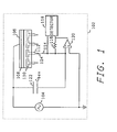
- Fig. 1 shows a schematic diagram of an alternative embodiment the invention.
- the system of one embodiment of the present invention 102 uses an oscillator 104 which supplies an alternating current signal, typically eight kiloHertz (8 Khz) at three (3) volts.
- the output of the oscillator 104 is connected to a metallic electrode 106 which is placed on top of an integrated circuit package 110.
- An insulator 108 may be placed between the electrode 106 and the integrated circuit package 110.
- a terminal pin under test 112 is connected to an integrated circuit trace 114 which is connected to a current measuring circuit.
- the connection to the current measuring circuit is typically made through a bed of nails connecting device.
- the current measuring circuit has an operational amplifier 120 with a feedback resistor 116.
- a detector 118 typically a voltmeter, is connected across the resistor 116 to measure the voltage drop, and thus the current flowing through the resistor 116.
- the current flowing through the resistor 116 is proportional to the current flowing through trace 114.
- the current measured must be greater than the amount of current that would flow through the baseline capacitance of the measurement system, represented by capacitor C bas 122.
- the current measuring circuit also determines the amount of capacitance that exists between the probe and the pin. As is well known in the art, since the frequency of the oscillator 104 is known, the capacitance can be calculated directly from the amount of current flowing in board trace 114. The capacitance between the probe and the pin is the calculated capacitance less the amount of capacitance in baseline capacitor 122.
- the oscillator 104 is activated and a current is conducted to the electrode 106.
- the current is passed to the pin 112 of the integrated circuit 110.
- the current then passes through a connection to a circuit assembly trace 114 and the current then passes to the circuit 116, 118 and 120 which measures the amount of current flowing from the pin 112 by measuring the voltage across resistor 116. If a threshold amount of current is measured by the circuit, that is, the current measured is greater than the amount of current flowing through C bas 122 alone, then the pin 112 must be connected to the integrated circuit trace 114.
- the pin 112 is not connected at location 124, no current will be conducted to the integrated circuit trace 114 and the threshold amount of current will not be measured by the circuit, indicating that a pin open fault is present.
- the detector 118 provides an indication to an operator oft the system that the pin is or is not connected.
- a voltage measurement circuit is connected between the probe 106 and the circuit trace 114 to measure the voltage across the capacitor formed by the probe and the pin. This measured voltage is used to calculate the capacitance formed and if the capacitance is equal to C bas alone, then a fault is present.
- Fig. 2 shows a top cut away view of the integrated circuit 110 and the electrode 106
- Fig. 3 shows a side cut away view of the integrated circuit 110 and the electrode 106.
- Figs. 2 and 3 illustrate how the capacitive coupling occurs between the electrode and the pins of the integrated circuit.
- the integrated circuit package 110 contains an integrated circuit 202.
- the integrated circuit 202 contains connections, however, these connections must be made to the outside of the integrated circuit package 110. Therefore, the pin 112 is connected to an internal conductor 204 which connects the pin 112 to a location just adjacent the integrated circuit 202. There a small wire spans between the conductor 204 and a location on the integrated circuit 202. Similar connections are made to all the other pins of the integrated circuit package 110.
- the conductor 204 forms a conductive plate, which acts as one plate of a capacitor.
- the other plate of the capacitor is the electrode 106, here illustrated by dashed lines, indicating that the conductor 106 is placed over the top of the integrated circuit package 110.
- the capacitor created in this manner is small, it is sufficient to conduct a signal from the electrode 106 to the pin 112.
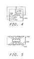
- FIG. 4 shows a diagram of an integrated circuit having four pins tied together.
- an integrated circuit 402 contains four leads within the package that are tied together. Lead 404, lead 406, lead 408, and lead 410 are all connected to a common point 412 within the integrated circuit 402. This presents a testing problem, since it is difficult to detect when one or some, but not all, of the pins connected to the leads 404, 406, 408, and 410 are not making contact with the circuit assembly.
- the circuit of Fig. 1 to measure the amount of capacitance between a probe and a lead, multiple leads tied together can be analyzed.
- the amount of capacitance between the four pins of the integrated circuit 402 and a probe would be measured using a circuit that is known to be functioning correctly. This amount of capacitance will have a particular value, for example, 200 femtofarads.
- the pins of the integrated circuit 402 are then intentionally disconnected, one at a time, and the amount of capacitance measured again. Using this method, the amount of capacitance of each pin can be determined. For example, the capacitance might be measured as follows:
- the capacitance When an unknown circuit is tested, if any one pin is not connected, the capacitance will be less than the amount measured for all four pins, indicating a fault. In addition, if pin 404 is not making contact, the capacitance will be a unique value, because of the unique amount of capacitance created by pin 404. Thus, in some cases, the difference in the capacitance will allow the technique to determine exactly which pin is not making contact.
- the measured capacitance would be 135 femtofarads, indicating that only pin 404 could be responsible for the decreased capacitance.
- This technique is ineffective if the pins are connected to the device substrate through a low impedance path. In this case, all the pins must be unconnected before the technique can detect a lowered capacitance.
- FIG. 5 shows a diagram of such a probe placed over an integrated circuit.
- an integrated circuit 502 has a pin 504 with a very small probe 506 placed over top of the pin 504.
- each pin can be probed separately.
- This technique results in much smaller capacitance being measured, however. For example, in one test of this technique, connected pins measured a capacitance of approximately 50 femtofarads, whereas unconnected pins measured 15 femtofarads.
- a probe 602 has a number of very small segments, such as segment 604, each of which will be located over a single pin when the probe 602 is placed on top of an integrated circuit.
- Each of the segments is connected to one output of a selector 606, to select a single segment when testing, and the input to the selector is connected to the voltage source 608.
- the measuring device is connected in the same manner as Fig. 1.
- a fairly large signal typically three volts, is applied to the probe placed on top of the integrated circuit. This is generally not the preferred way of testing a pin because of the large voltage that can be used. However, if the pin being tested is also connected to a pull-up resistor, or any resistor tied to a node which may be grounded, a reversal of the source and detector in the circuit of Fig. 1 may be desirable.
- a source 704 which is typically 0.2 volts RMS, is connected to the integrated circuit pin which forms one plate of the probe capacitor 710.
- Resistor 706 represents the pull-up resistor that may be inside or outside inside the integrated circuit 718.
- the baseline system capacitance 708 is always in parallel with the capacitor formed by the probe 710 and the terminal pin 720. These two capacitors are connected to the measurement circuit which includes the op-amp 716, feedback resistor 714, and detector 712. Because of the low voltage of the source 704, that is, approximately 0.2 volts RMS, junction diodes within the integrated circuit being tested are not forward biased enough to overload the source.
- Fig. 8 shows a schematic diagram of the circuit of Fig. 1 with the addition of pin guarding.
- the test circuit 802 contains a signal source 804 which is connected to a probe 806, placed over an integrated circuit 810.
- Signal capacitively coupled from the probe 806 to a pin 812 is conducted through a conductor 814 to a current measuring circuit which includes an op-amp 820, a feedback resistor 816, and a detector 818.
- a current measuring circuit which includes an op-amp 820, a feedback resistor 816, and a detector 818.
- all the pins of integrated circuit 810 that are not being tested are grounded through ground connections 822 and 824. This grounding of unused pins is called "guarding".
- FIG. 9 shows a diagram of such a shield in place over the probe.
- an integrated circuit 110 contains the capacitive probe 106 as illustrated previously in Fig. 1.
- a shield 902 is placed over the probe 106 but not contacting the probe 106.
- the shield 902 also contains a skirt 904 which extends outside the probe 106 and down over a part of the pins of the integrated circuit 110.
- the probe 106 may also placed in contact with any heat sink which is located on top of the integrated circuit 110. If the heat sink is not grounded, the probe may contact or couple to the heat sink, which enhances the coupling between the probe and the lead frame. However, if the heat sink is grounded, the leads within the integrated circuit will effectively be shielded from the capacitive probe and no capacitance can be measured. In these situations, the integrated circuit must be tested prior to grounding the heat sink.
- Fig. 10 shows an alternative embodiment having the measurement system connected to the probe, as in Fig. 7, but also including an amplifier in the probe circuit.
- a source 1004 which is typically 0.2 volts RMS, is connected to a selector 1005, and an output of the selector 1005 is connected to a pin 1020 of an integrated circuit 1006.
- the probe 1008 is placed adjacent the integrated circuit 1006 and is connected to a multiplexer 1010.
- the output of the multiplexer 1010 is connected to an amplifier 1014 having a large feedback resistor 1016.
- the multiplexer could be controlled by a switch or it could be controlled electrically by a controller or computer system.
- the output of the amplifier 1014 is connected to a detector 1018 to measure the current or voltage across the capacitance formed by the probe 1008 and the pin 1020.
- a shield 1028 may also be placed over the integrated circuit 1006 in the manner described above with respect to Fig. 9.
- the amplifier 1014 may also be placed inside the shield 1028.
- a second integrated circuit 1022 can also be tested.
- the source 1004 is also connected to pin 1024 of the integrated circuit 1022 through the selector 1005, and a second probe 1030 is placed adjacent the integrated circuit 1022. This second probe 1030 is connected to another input of the multiplexer 1010.
- the multiplexer 1010 and the selector 1005 are controlled by a controller 1032.
- a second shield 1026 may be placed over the second integrated circuit 1022.
- the amplifier 1014 in the probe circuit reduces sensitivity to noise and reduces the effects of system capacitance.
- the amplifiercould be located inside the detector 1018 or an amplifier could be placed between each of the probes and the multiplexer 1010.
- Another technique to reduce noise when testing an integrated circuit using the method of the present invention is to guard all ground and power pins of the integrated circuit. This technique is particularly effective since this usually grounds the printed circuit board ground plane which is also connected to many pins on other integrated circuits, thus reducing overall system noise.
- circuits described above are shown testing an electrical component such as an integrated circuit, the technique will work equally well with mechanical components such as integrated circuit sockets. It will also work with analog electrical components or discrete components such as resistors and capacitors.
Landscapes
- Physics & Mathematics (AREA)
- General Physics & Mathematics (AREA)
- Engineering & Computer Science (AREA)
- General Engineering & Computer Science (AREA)
- Testing Of Short-Circuits, Discontinuities, Leakage, Or Incorrect Line Connections (AREA)
- Tests Of Electronic Circuits (AREA)
- Testing Of Individual Semiconductor Devices (AREA)
Abstract
Description
- This invention relates to measuring and testing devices and more particularly to in-circuit testing devices. Even more particularly, the invention relates to in-circuit testing of connections between an integrated circuit and a printed circuit board.
- It is important that electronic components and printed circuit boards be tested after the components have been soldered to the printed circuit boards. Several different approaches have been developed for testing the components and printed circuit boards, including functional testing, in-circuit testing, and manufacturing defect analyzers.
- Functional testing uses a procedure of applying predetermined input signals and monitoring the output of a printed circuit board to determine if all of the components are present and operating properly on the circuit board. While functional testing provides a way of determining whether the P.C. board is functioning properly, it provides little or no information regarding the functioning of individual components on the board. Complex programming techniques have been used to provide limited information as to the location of non-functioning components on the board by carefully selecting input data and analyzing the output results. Such systems are complex, often costly to implement, and normally provide only vague information as to the location of malfunctioning components.
- Because of the limitations of functional testing, in-circuit testing techniques have been used to individually test the components on the printed circuit board to determine if these components are working properly. This process uses a "bed of nails" tester to access each individual component and test that component individually. In this manner, non-functioning components can be identified and replaced to prevent the entire circuit board from being scrapped. This process works well for simple components where the circuit inside the component is known and can be easily tested. If the component being tested is very complex, or if the circuit inside the component is unknown, in-circuit testing may not achieve satisfactory results.
- Manufacturing defect analyzers are another class of testing devices that provide simpler tests and are less expensive to implement. These devices are designed to locate manufacturing faults, such as shorts on a printed circuit board, missing integrated circuits, bent component pins, etc. Although these devices do a reasonably good job of finding shorts and gross analog faults, they are marginal when testing digital sections of the board.
- One very important potential problem that must be tested on every printed circuit board is whether all the pins of every component are soldered to the circuit board. Functional testing may miss a particular pin, if the functions performed by that particular pin are not thoroughly tested in functional test. Testing for this type of fault is particularly difficult when the circuit inside the component is unknown, such as the case with application specific integrated circuits (AS- lCs). Because of the large number of ASICs and the complexity of these devices, it is often not feasible to design an in-circuit test or a functional test to isolate this particular component.
- There is need in the art then for a device and method which will determine whether all pins of a component are soldered to a circuit board. There is further need in the art for such a device and method which does not rely on the circuit contained in the component. The present invention meets these and other needs.
- This application is related to the disclosure of US-A-5124660 entitled Identification of Pin-Open Faults by Capacitive Coupling through the Integrated Circuit, which is incorporated herein by reference for all that is disclosed therein.
- It is an aspect of the present invention to provide an apparatus and method to test for a connection between a pin of a component and a circuit assembly to which it is attached.
- It is another aspect of the invention to provide such an apparatus and method that does not rely on the circuit contained inside the component.
- The above and other aspects of the present invention are accomplished in a system that overcomes the disadvantages and limitations of the prior art by providing an apparatus and method for determining whether analog, digital, discrete or non-electrical components are present and properly connected to a printed circuit board. The present invention determines whether terminal pins, including input, output, power and ground, are connected to the circuit assembly regardless of the component family being used.
- Specifically, the invention uses a metallic probe, such as copper plate, placed on top of an integrated circuit package. A connection is then made, through a bed of nails tester or other means, to a circuit assembly wiring trace that connects to the pin being tested. This connection is in turn connected to an oscillator, and an output of the probe is connected to a measuring device. The oscillator is then set to supply a signal to the pin, and this signal is capacitively coupled through the component package to the probe. Current is measured flowing out of the probe onto the measuring device, and if this current exceeds a predetermined threshold, the pin is considered to be connected. This system may also include an amplifier between the probe and the measurement device to reduce sensitivity to noise, and eliminate any unwanted system capacitance.
- An alternative embodiment measures the capacitance between the metallic probe and the lead within the integrated circuit, and if the capacitance exceeds the base capacitance of the system by a predetermined amount, the pin is considered connected. The system may also measure voltage between the probe and pin to determine capacitance. Where multiple pins are tied together inside the integrated circuit, the capacitance of all the pins is compared against a threshold capacitance. Unused pins may be grounded to minimize their effect on the capacitance. The probe may be shielded to minimize stray capacitance. A segmented probe, which has a separate segment over each pin of the integrated circuit may be used to further isolate a single pin.
- In another alternative embodiment the voltage or current source to connected to the probe and the measuring system is connected to the pin.
- The above and other objects, features, and advantages of the invention will be better understood by reading the following more particular description of the invention, presented in conjunction with the following drawings, wherein:
- Fig. 1 shows a schematic diagram of the invention;
- Fig. 2 shows a top cutaway view of an integrated circuit;
- Fig. 3 shows a side cutaway view of an integrated circuit and illustrates, along with Fig. 2, how the capacitive coupling occurs;
- Fig. 4 shows an integrated circuit having several pins connected externally outside the integrated circuit;
- Fig. 5 shows the use of a very small probe that can be placed over a single pin of an integrated circuit;
- Fig. 6 shows a segmented probe that is used to separately test each pin of an integrated circuit;
- Fig. 7 shows a schematic diagram of the preferred embodiment of the invention wherein the component connections reversed from Fig. 1;
- Fig. 8 shows a schematic diagram of the invention with unused pins grounded;
- Fig. 9 shows a diagram of the probe with a shield; and
- Fig. 10 shows a schematic diagram having the measurement system connected to the probe.
- The following description is of the best presently contemplated mode of carrying out the present invention. This description is not to be taken in a limiting sense but is made merely for the purpose of describing the general principles of the invention. The scope of the invention should be determined by referencing the appended claims.
- Fig. 1 shows a schematic diagram of an alternative embodiment the invention. The preferred em- bodimentwill be described below with respect to Figs. 7 and 10. Referring now to Fig. 1, the system of one embodiment of the
present invention 102 uses anoscillator 104 which supplies an alternating current signal, typically eight kiloHertz (8 Khz) at three (3) volts. The output of theoscillator 104 is connected to ametallic electrode 106 which is placed on top of anintegrated circuit package 110. Aninsulator 108 may be placed between theelectrode 106 and theintegrated circuit package 110. A terminal pin undertest 112 is connected to anintegrated circuit trace 114 which is connected to a current measuring circuit. The connection to the current measuring circuit is typically made through a bed of nails connecting device. - The current measuring circuit has an
operational amplifier 120 with afeedback resistor 116. Adetector 118, typically a voltmeter, is connected across theresistor 116 to measure the voltage drop, and thus the current flowing through theresistor 116. The current flowing through theresistor 116 is proportional to the current flowing throughtrace 114. The current measured must be greater than the amount of current that would flow through the baseline capacitance of the measurement system, represented bycapacitor C bas 122. - The current measuring circuit also determines the amount of capacitance that exists between the probe and the pin. As is well known in the art, since the frequency of the
oscillator 104 is known, the capacitance can be calculated directly from the amount of current flowing inboard trace 114. The capacitance between the probe and the pin is the calculated capacitance less the amount of capacitance inbaseline capacitor 122. - To perform the test, the
oscillator 104 is activated and a current is conducted to theelectrode 106. Through capacitive coupling, the current is passed to thepin 112 of theintegrated circuit 110. The current then passes through a connection to acircuit assembly trace 114 and the current then passes to thecircuit pin 112 by measuring the voltage acrossresistor 116. If a threshold amount of current is measured by the circuit, that is, the current measured is greater than the amount of current flowing throughC bas 122 alone, then thepin 112 must be connected to theintegrated circuit trace 114. If thepin 112 is not connected atlocation 124, no current will be conducted to theintegrated circuit trace 114 and the threshold amount of current will not be measured by the circuit, indicating that a pin open fault is present. Thedetector 118 provides an indication to an operator oft the system that the pin is or is not connected. - In an alternative embodiment (not shown), a voltage measurement circuit is connected between the
probe 106 and thecircuit trace 114 to measure the voltage across the capacitor formed by the probe and the pin. This measured voltage is used to calculate the capacitance formed and if the capacitance is equal to Cbas alone, then a fault is present. - Fig. 2 shows a top cut away view of the
integrated circuit 110 and theelectrode 106, and Fig. 3 shows a side cut away view of theintegrated circuit 110 and theelectrode 106. Figs. 2 and 3 illustrate how the capacitive coupling occurs between the electrode and the pins of the integrated circuit. Referring now to Figs. 2 and 3, theintegrated circuit package 110 contains anintegrated circuit 202. Theintegrated circuit 202 contains connections, however, these connections must be made to the outside of theintegrated circuit package 110. Therefore, thepin 112 is connected to aninternal conductor 204 which connects thepin 112 to a location just adjacent theintegrated circuit 202. There a small wire spans between theconductor 204 and a location on theintegrated circuit 202. Similar connections are made to all the other pins of theintegrated circuit package 110. - The
conductor 204 forms a conductive plate, which acts as one plate of a capacitor. The other plate of the capacitor is theelectrode 106, here illustrated by dashed lines, indicating that theconductor 106 is placed over the top of theintegrated circuit package 110. Although the capacitor created in this manner is small, it is sufficient to conduct a signal from theelectrode 106 to thepin 112. - Occasionally, multiple pins within an integrated circu it wil be tied together. For example, this often occurs if an integrated circuit has multiple ground pins or multiple pins for a particular signal. Fig. 4 shows a diagram of an integrated circuit having four pins tied together. Referring now to Fig. 4, an
integrated circuit 402 contains four leads within the package that are tied together. Lead 404, lead 406, lead 408, and lead 410 are all connected to acommon point 412 within theintegrated circuit 402. This presents a testing problem, since it is difficult to detect when one or some, but not all, of the pins connected to theleads - Initially, the amount of capacitance between the four pins of the
integrated circuit 402 and a probe would be measured using a circuit that is known to be functioning correctly. This amount of capacitance will have a particular value, for example, 200 femtofarads. The pins of theintegrated circuit 402 are then intentionally disconnected, one at a time, and the amount of capacitance measured again. Using this method, the amount of capacitance of each pin can be determined. For example, the capacitance might be measured as follows: - pin 404 - 65 femtofarads
- pin 406 - 45 femtofarads
- pin 408 - 45 femtofarads
- pin 410 - 45 femtofarads
- When an unknown circuit is tested, if any one pin is not connected, the capacitance will be less than the amount measured for all four pins, indicating a fault. In addition, if
pin 404 is not making contact, the capacitance will be a unique value, because of the unique amount of capacitance created bypin 404. Thus, in some cases, the difference in the capacitance will allow the technique to determine exactly which pin is not making contact. - In the above example, if
pin 404 is not making contact, the measured capacitance would be 135 femtofarads, indicating thatonly pin 404 could be responsible for the decreased capacitance. This technique, however, is ineffective if the pins are connected to the device substrate through a low impedance path. In this case, all the pins must be unconnected before the technique can detect a lowered capacitance. - Another method will also solve the problem depicted by Fig. 4. That method is the use of a very small probe which covers only the surface area of a single pin. Fig. 5 shows a diagram of such a probe placed over an integrated circuit. Referring now to Fig. 5, an
integrated circuit 502 has apin 504 with a verysmall probe 506 placed over top of thepin 504. By moving thesmaller probe 506 around the top of theintegrated circuit 502, each pin can be probed separately. This technique results in much smaller capacitance being measured, however. For example, in one test of this technique, connected pins measured a capacitance of approximately 50 femtofarads, whereas unconnected pins measured 15 femtofarads. - The technique of Fig. 5 can be extended by creating a segmented probe as shown in Fig. 6. Referring now to Fig. 6, a
probe 602 has a number of very small segments, such assegment 604, each of which will be located over a single pin when theprobe 602 is placed on top of an integrated circuit. Each of the segments is connected to one output of aselector 606, to select a single segment when testing, and the input to the selector is connected to thevoltage source 608. When using the segmentedprobe 602, the measuring device is connected in the same manner as Fig. 1. - In the circuit of Fig. 1, a fairly large signal, typically three volts, is applied to the probe placed on top of the integrated circuit. This is generally not the preferred way of testing a pin because of the large voltage that can be used. However, if the pin being tested is also connected to a pull-up resistor, or any resistor tied to a node which may be grounded, a reversal of the source and detector in the circuit of Fig. 1 may be desirable.
- A circuit implementing this reversal is shown in Fig. 7, which is the preferred embodiment. Referring now to Fig. 7, a
source 704, which is typically 0.2 volts RMS, is connected to the integrated circuit pin which forms one plate of theprobe capacitor 710. Resistor 706 represents the pull-up resistor that may be inside or outside inside theintegrated circuit 718. Thebaseline system capacitance 708 is always in parallel with the capacitor formed by theprobe 710 and theterminal pin 720. These two capacitors are connected to the measurement circuit which includes the op-amp 716,feedback resistor 714, anddetector 712. Because of the low voltage of thesource 704, that is, approximately 0.2 volts RMS, junction diodes within the integrated circuit being tested are not forward biased enough to overload the source. - Fig. 8 shows a schematic diagram of the circuit of Fig. 1 with the addition of pin guarding. Referring now to Fig. 8, the
test circuit 802 contains asignal source 804 which is connected to aprobe 806, placed over anintegrated circuit 810. Signal capacitively coupled from theprobe 806 to a pin 812 is conducted through aconductor 814 to a current measuring circuit which includes an op-amp 820, afeedback resistor 816, and adetector 818. In the circuit of Fig. 8, unlike the circuit of Fig. 1, all the pins ofintegrated circuit 810 that are not being tested, are grounded throughground connections - Another technique for reducing cross-talk and noise is to place a grounded shield over the probe. Fig. 9 shows a diagram of such a shield in place over the probe. Referring now to Fig. 9, an
integrated circuit 110 contains thecapacitive probe 106 as illustrated previously in Fig. 1. In addition, however, ashield 902 is placed over theprobe 106 but not contacting theprobe 106. Theshield 902 also contains askirt 904 which extends outside theprobe 106 and down over a part of the pins of theintegrated circuit 110. - The probe 106 (Fig. 1) may also placed in contact with any heat sink which is located on top of the
integrated circuit 110. If the heat sink is not grounded, the probe may contact or couple to the heat sink, which enhances the coupling between the probe and the lead frame. However, if the heat sink is grounded, the leads within the integrated circuit will effectively be shielded from the capacitive probe and no capacitance can be measured. In these situations, the integrated circuit must be tested prior to grounding the heat sink. - Fig. 10 shows an alternative embodiment having the measurement system connected to the probe, as in Fig. 7, but also including an amplifier in the probe circuit. Referring now to Fig. 10, a
source 1004, which is typically 0.2 volts RMS, is connected to aselector 1005, and an output of theselector 1005 is connected to apin 1020 of anintegrated circuit 1006. Theprobe 1008 is placed adjacent theintegrated circuit 1006 and is connected to amultiplexer 1010. The output of themultiplexer 1010 is connected to anamplifier 1014 having alarge feedback resistor 1016. The multiplexer could be controlled by a switch or it could be controlled electrically by a controller or computer system. The output of theamplifier 1014 is connected to adetector 1018 to measure the current or voltage across the capacitance formed by theprobe 1008 and thepin 1020. Ashield 1028 may also be placed over theintegrated circuit 1006 in the manner described above with respect to Fig. 9. Theamplifier 1014 may also be placed inside theshield 1028. - A second
integrated circuit 1022 can also be tested. Thesource 1004 is also connected to pin 1024 of theintegrated circuit 1022 through theselector 1005, and asecond probe 1030 is placed adjacent theintegrated circuit 1022. Thissecond probe 1030 is connected to another input of themultiplexer 1010. Themultiplexer 1010 and theselector 1005 are controlled by acontroller 1032. Asecond shield 1026 may be placed over the secondintegrated circuit 1022. - Having the
amplifier 1014 in the probe circuit reduces sensitivity to noise and reduces the effects of system capacitance. Alternatively, the amplifiercould be located inside thedetector 1018 or an amplifier could be placed between each of the probes and themultiplexer 1010. - Another technique to reduce noise when testing an integrated circuit using the method of the present invention, is to guard all ground and power pins of the integrated circuit. This technique is particularly effective since this usually grounds the printed circuit board ground plane which is also connected to many pins on other integrated circuits, thus reducing overall system noise.
- Although the circuits described above are shown testing an electrical component such as an integrated circuit, the technique will work equally well with mechanical components such as integrated circuit sockets. It will also work with analog electrical components or discrete components such as resistors and capacitors.
- Having thus described a presently preferred embodiment of the present invention, it will now be appreciated that the objects of the invention have been fully achieved, and it will be understood by those skilled in the art that many changes in construction and circuitry and widely differing embodiments and applications of the invention will suggest themselves without departing from the spirit and scope of the present invention. The disclosures and the description herein are intended to be illustrative and are not in any sense limiting of the invention, more preferably defined in scope by the following claims.
Claims (10)
Applications Claiming Priority (2)
| Application Number | Priority Date | Filing Date | Title |
|---|---|---|---|
| US07/848,909 US5696451A (en) | 1992-03-10 | 1992-03-10 | Identification of pin-open faults by capacitive coupling |
| US848909 | 1992-03-10 |
Publications (3)
| Publication Number | Publication Date |
|---|---|
| EP0560484A2 true EP0560484A2 (en) | 1993-09-15 |
| EP0560484A3 EP0560484A3 (en) | 1994-06-08 |
| EP0560484B1 EP0560484B1 (en) | 2000-10-18 |
Family
ID=25304605
Family Applications (1)
| Application Number | Title | Priority Date | Filing Date |
|---|---|---|---|
| EP93300832A Expired - Lifetime EP0560484B1 (en) | 1992-03-10 | 1993-02-04 | Identification of pin-open faults by capacitive coupling |
Country Status (6)
| Country | Link |
|---|---|
| US (1) | US5696451A (en) |
| EP (1) | EP0560484B1 (en) |
| JP (1) | JP3228816B2 (en) |
| KR (1) | KR100248640B1 (en) |
| DE (1) | DE69329567T2 (en) |
| TW (2) | TW209317B (en) |
Cited By (5)
| Publication number | Priority date | Publication date | Assignee | Title |
|---|---|---|---|---|
| EP0573159A2 (en) * | 1992-06-03 | 1993-12-08 | Hewlett-Packard Company | Identification of pin-open faults by capacitive coupling through the integrated circuit package |
| EP0599544A1 (en) * | 1992-11-25 | 1994-06-01 | Hewlett-Packard Company | Capacitive electrode system for detecting open solder joints in printed circuit assemblies |
| EP0618453A2 (en) * | 1993-03-26 | 1994-10-05 | ARNOLD EDV GmbH | Method of testing circuit boards and device for carrying out the method |
| DE4402230C1 (en) * | 1994-01-26 | 1995-01-19 | Gfp Ges Fuer Prueftechnik Mbh | Method for testing whether terminal pins (posts) of an integrated circuit are electrically conductively soldered into a printed circuit and circuit arrangement for carrying out the method |
| EP0653642A1 (en) * | 1993-10-19 | 1995-05-17 | Hewlett-Packard Company | System for measuring the integrity of an electrical contact |
Families Citing this family (32)
| Publication number | Priority date | Publication date | Assignee | Title |
|---|---|---|---|---|
| US5391993A (en) * | 1994-01-27 | 1995-02-21 | Genrad, Inc. | Capacitive open-circuit test employing threshold determination |
| JP2994259B2 (en) | 1996-03-28 | 1999-12-27 | オー・エイチ・ティー株式会社 | Substrate inspection method and substrate inspection device |
| JP3165056B2 (en) * | 1997-02-28 | 2001-05-14 | 日本電産リード株式会社 | Substrate inspection device and substrate inspection method |
| FR2771182B1 (en) * | 1997-11-18 | 2000-01-28 | Sgs Thomson Microelectronics | METHOD AND SYSTEM FOR TESTING AN INTEGRATED CIRCUIT WITH CONTACTLESS OPERATION, AND AN INPUT CAPACITY OF SUCH AN INTEGRATED CIRCUIT |
| WO1999040448A1 (en) * | 1998-02-05 | 1999-08-12 | Koninklijke Philips Electronics N.V. | Connection test method |
| JP3675678B2 (en) * | 1999-08-06 | 2005-07-27 | 株式会社 東京ウエルズ | Probe contact state detection method and probe contact state detection device |
| US6262580B1 (en) * | 1999-10-14 | 2001-07-17 | United Microelectronics Corp | Method and testing system for measuring contact resistance for pin of integrated circuit |
| JP2001235501A (en) * | 2000-02-22 | 2001-08-31 | Oht Inc | Inspection device and sensor |
| KR20020019951A (en) * | 2000-05-19 | 2002-03-13 | 이시오까 쇼오고 | Method and apparatus for circuit board continuity test, tool for continuity test, and recording medium |
| US6333680B1 (en) * | 2000-10-02 | 2001-12-25 | International Business Machines Corporation | Method and system for characterizing coupling capacitance between integrated circuit interconnects |
| US6683449B1 (en) * | 2000-10-06 | 2004-01-27 | Dell Products, L.P. | Apparatus and method for detecting a mechanical component on a computer system substrate |
| US20030115502A1 (en) * | 2001-12-14 | 2003-06-19 | Smiths Industries Aerospace & Defense Systems, Inc. | Method of restoring encapsulated integrated circuit devices |
| US6717415B2 (en) * | 2002-02-05 | 2004-04-06 | Logicvision, Inc. | Circuit and method for determining the location of defect in a circuit |
| US6947853B2 (en) * | 2002-05-23 | 2005-09-20 | Oht, Inc. | Apparatus and method for inspecting electrical continuity of circuit board, jig for use therein, and recording medium thereon |
| US7109728B2 (en) * | 2003-02-25 | 2006-09-19 | Agilent Technologies, Inc. | Probe based information storage for probes used for opens detection in in-circuit testing |
| US6901336B2 (en) * | 2003-03-31 | 2005-05-31 | Agilent Technologies, Inc. | Method and apparatus for supplying power, and channeling analog measurement and communication signals over single pair of wires |
| US7170394B2 (en) * | 2003-07-31 | 2007-01-30 | Agilent Technologies, Inc. | Remote current sensing and communication over single pair of power feed wires |
| US6930494B2 (en) * | 2003-08-29 | 2005-08-16 | Agilent Technologies, Inc. | Capacitive probe assembly with flex circuit |
| US6998849B2 (en) * | 2003-09-27 | 2006-02-14 | Agilent Technologies, Inc. | Capacitive sensor measurement method for discrete time sampled system for in-circuit test |
| US7224169B2 (en) | 2004-11-02 | 2007-05-29 | Agilent Technologies, Inc. | Methods and apparatus for non-contact testing and diagnosing of inaccessible shorted connections |
| KR100674450B1 (en) * | 2005-03-31 | 2007-02-15 | 주식회사 청천바텍 | Appartatus for drying and carbonizing for waste matter |
| US7279921B1 (en) * | 2005-06-08 | 2007-10-09 | National Semiconductor Corporation | Apparatus and method for testing power and ground pins on a semiconductor integrated circuit |
| US7622931B2 (en) * | 2005-10-03 | 2009-11-24 | University Of Utah Research Foundation | Non-contact reflectometry system and method |
| TWI320485B (en) * | 2007-03-08 | 2010-02-11 | Test Research Inc | Open-circuit testing system and method |
| US7764069B2 (en) * | 2007-04-25 | 2010-07-27 | International Business Machines Corporation | Process for measuring bond-line thickness |
| US8310256B2 (en) | 2009-12-22 | 2012-11-13 | Teradyne, Inc. | Capacitive opens testing in low signal environments |
| US8760185B2 (en) * | 2009-12-22 | 2014-06-24 | Anthony J. Suto | Low capacitance probe for testing circuit assembly |
| JP5307085B2 (en) * | 2010-07-20 | 2013-10-02 | 日置電機株式会社 | Circuit board inspection equipment |
| US8583391B2 (en) * | 2011-04-15 | 2013-11-12 | Hamilton Sundstrand Corporation | Monitoring the low cycle fatigue of ruggedized avionics electronics |
| KR102328803B1 (en) * | 2014-12-16 | 2021-11-22 | 삼성전자주식회사 | Electronic device and method for determining an abnormal state of a connector |
| US11879935B2 (en) * | 2020-09-25 | 2024-01-23 | Nokomis, Inc. | Testing of microelectronics device and method |
| KR102547616B1 (en) * | 2021-04-15 | 2023-06-26 | 큐알티 주식회사 | Board for testing of semiconductor chip, and test system of semiconductor chip, and test method of semiconductor chip |
Citations (5)
| Publication number | Priority date | Publication date | Assignee | Title |
|---|---|---|---|---|
| EP0177210A1 (en) * | 1984-09-14 | 1986-04-09 | Gec-Marconi Limited | Electric circuit testing equipment |
| GB2179751A (en) * | 1985-08-23 | 1987-03-11 | Bicc Plc | Terminating electrical connectors |
| EP0317440A1 (en) * | 1987-11-20 | 1989-05-24 | Thomson-Csf | Device for controling a soldering joint by electronic mesurement of the soldering joint area |
| US4918376A (en) * | 1989-03-07 | 1990-04-17 | Ade Corporation | A.C. capacitive gauging system |
| US5124660A (en) * | 1990-12-20 | 1992-06-23 | Hewlett-Packard Company | Identification of pin-open faults by capacitive coupling through the integrated circuit package |
Family Cites Families (6)
| Publication number | Priority date | Publication date | Assignee | Title |
|---|---|---|---|---|
| GB2143954A (en) * | 1983-07-22 | 1985-02-20 | Sharetree Ltd | A capacitive method and apparatus for checking connections of a printed circuit board |
| US4789829A (en) * | 1986-07-18 | 1988-12-06 | Science Application International Corporation | Method and apparatus for determining RE gasket shielding effectiveness |
| US4779041A (en) * | 1987-05-20 | 1988-10-18 | Hewlett-Packard Company | Integrated circuit transfer test device system |
| US5557209A (en) * | 1990-12-20 | 1996-09-17 | Hewlett-Packard Company | Identification of pin-open faults by capacitive coupling through the integrated circuit package |
| US5254953A (en) * | 1990-12-20 | 1993-10-19 | Hewlett-Packard Company | Identification of pin-open faults by capacitive coupling through the integrated circuit package |
| US5266901A (en) * | 1992-05-29 | 1993-11-30 | International Business Machines Corp. | Apparatus and method for resistive detection and waveform analysis of interconenction networks |
-
1992
- 1992-03-10 US US07/848,909 patent/US5696451A/en not_active Expired - Lifetime
- 1992-10-15 TW TW081108206A patent/TW209317B/zh active
- 1992-10-15 TW TW082103079A patent/TW239251B/zh active
-
1993
- 1993-02-04 DE DE69329567T patent/DE69329567T2/en not_active Expired - Fee Related
- 1993-02-04 EP EP93300832A patent/EP0560484B1/en not_active Expired - Lifetime
- 1993-03-09 KR KR1019930003506A patent/KR100248640B1/en not_active IP Right Cessation
- 1993-03-10 JP JP07629693A patent/JP3228816B2/en not_active Expired - Fee Related
Patent Citations (6)
| Publication number | Priority date | Publication date | Assignee | Title |
|---|---|---|---|---|
| EP0177210A1 (en) * | 1984-09-14 | 1986-04-09 | Gec-Marconi Limited | Electric circuit testing equipment |
| GB2179751A (en) * | 1985-08-23 | 1987-03-11 | Bicc Plc | Terminating electrical connectors |
| EP0317440A1 (en) * | 1987-11-20 | 1989-05-24 | Thomson-Csf | Device for controling a soldering joint by electronic mesurement of the soldering joint area |
| US4918376A (en) * | 1989-03-07 | 1990-04-17 | Ade Corporation | A.C. capacitive gauging system |
| US5124660A (en) * | 1990-12-20 | 1992-06-23 | Hewlett-Packard Company | Identification of pin-open faults by capacitive coupling through the integrated circuit package |
| EP0492806A2 (en) * | 1990-12-20 | 1992-07-01 | Hewlett-Packard Company | Identification of pin-open faults by capacitive coupling through the integrated circuit package |
Cited By (10)
| Publication number | Priority date | Publication date | Assignee | Title |
|---|---|---|---|---|
| US5625292A (en) * | 1990-12-20 | 1997-04-29 | Hewlett-Packard Company | System for measuring the integrity of an electrical contact |
| EP0573159A2 (en) * | 1992-06-03 | 1993-12-08 | Hewlett-Packard Company | Identification of pin-open faults by capacitive coupling through the integrated circuit package |
| EP0573159A3 (en) * | 1992-06-03 | 1994-05-11 | Hewlett Packard Co | Identification of pin-open faults by capacitive coupling through the integrated circuit package |
| EP0599544A1 (en) * | 1992-11-25 | 1994-06-01 | Hewlett-Packard Company | Capacitive electrode system for detecting open solder joints in printed circuit assemblies |
| US5420500A (en) * | 1992-11-25 | 1995-05-30 | Hewlett-Packard Company | Pacitive electrode system for detecting open solder joints in printed circuit assemblies |
| EP0618453A2 (en) * | 1993-03-26 | 1994-10-05 | ARNOLD EDV GmbH | Method of testing circuit boards and device for carrying out the method |
| EP0618453A3 (en) * | 1993-03-26 | 1995-09-27 | Arnold Edv Gmbh | Method of testing circuit boards and device for carrying out the method. |
| EP0653642A1 (en) * | 1993-10-19 | 1995-05-17 | Hewlett-Packard Company | System for measuring the integrity of an electrical contact |
| DE4402230C1 (en) * | 1994-01-26 | 1995-01-19 | Gfp Ges Fuer Prueftechnik Mbh | Method for testing whether terminal pins (posts) of an integrated circuit are electrically conductively soldered into a printed circuit and circuit arrangement for carrying out the method |
| WO1995020766A1 (en) * | 1994-01-26 | 1995-08-03 | Gfp - Gesellschaft Für Prüftechnik Mbh | Process and device for testing printed circuit boards |
Also Published As
| Publication number | Publication date |
|---|---|
| JP3228816B2 (en) | 2001-11-12 |
| TW209317B (en) | 1993-07-11 |
| EP0560484B1 (en) | 2000-10-18 |
| US5696451A (en) | 1997-12-09 |
| JPH06160457A (en) | 1994-06-07 |
| KR930020165A (en) | 1993-10-19 |
| KR100248640B1 (en) | 2000-03-15 |
| DE69329567D1 (en) | 2000-11-23 |
| DE69329567T2 (en) | 2001-03-15 |
| EP0560484A3 (en) | 1994-06-08 |
| TW239251B (en) | 1995-01-21 |
Similar Documents
| Publication | Publication Date | Title |
|---|---|---|
| US5696451A (en) | Identification of pin-open faults by capacitive coupling | |
| US5124660A (en) | Identification of pin-open faults by capacitive coupling through the integrated circuit package | |
| US5557209A (en) | Identification of pin-open faults by capacitive coupling through the integrated circuit package | |
| US5254953A (en) | Identification of pin-open faults by capacitive coupling through the integrated circuit package | |
| EP0599544B1 (en) | Capacitive electrode system for detecting open solder joints in printed circuit assemblies | |
| US7075307B1 (en) | Method and apparatus for detecting shorts on inaccessible pins using capacitive measurements | |
| JP3784412B2 (en) | Manufacturing defect analyzer with expanded fault coverage | |
| US6087842A (en) | Integrated or intrapackage capability for testing electrical continuity between an integrated circuit and other circuitry | |
| US5517110A (en) | Contactless test method and system for testing printed circuit boards | |
| JP2625623B2 (en) | Circuit test apparatus and method | |
| US5138266A (en) | Single-probe charge measurement testing method | |
| US5625292A (en) | System for measuring the integrity of an electrical contact | |
| JPH01112179A (en) | Circuit board inspection instrument | |
| US6169395B1 (en) | Test for determining polarity of electrolytic capacitors within electronic assemblies | |
| WO2020055772A1 (en) | Method and apparatus for bond wire testing in an integrated circuit | |
| US11703549B2 (en) | Systems and methods for ground fault detection | |
| KR100476740B1 (en) | Method for testing rlc parallel circuit on the printed circuit board | |
| US9476928B2 (en) | System and method for detecting sensor leakage |
Legal Events
| Date | Code | Title | Description |
|---|---|---|---|
| PUAI | Public reference made under article 153(3) epc to a published international application that has entered the european phase |
Free format text: ORIGINAL CODE: 0009012 |
|
| AK | Designated contracting states |
Kind code of ref document: A2 Designated state(s): DE FR GB IT |
|
| PUAL | Search report despatched |
Free format text: ORIGINAL CODE: 0009013 |
|
| AK | Designated contracting states |
Kind code of ref document: A3 Designated state(s): DE FR GB IT |
|
| 17P | Request for examination filed |
Effective date: 19941130 |
|
| 17Q | First examination report despatched |
Effective date: 19970228 |
|
| GRAG | Despatch of communication of intention to grant |
Free format text: ORIGINAL CODE: EPIDOS AGRA |
|
| GRAG | Despatch of communication of intention to grant |
Free format text: ORIGINAL CODE: EPIDOS AGRA |
|
| GRAH | Despatch of communication of intention to grant a patent |
Free format text: ORIGINAL CODE: EPIDOS IGRA |
|
| GRAH | Despatch of communication of intention to grant a patent |
Free format text: ORIGINAL CODE: EPIDOS IGRA |
|
| GRAA | (expected) grant |
Free format text: ORIGINAL CODE: 0009210 |
|
| AK | Designated contracting states |
Kind code of ref document: B1 Designated state(s): DE FR GB IT |
|
| REF | Corresponds to: |
Ref document number: 69329567 Country of ref document: DE Date of ref document: 20001123 |
|
| ET | Fr: translation filed | ||
| ITF | It: translation for a ep patent filed |
Owner name: SOCIETA' ITALIANA BREVETTI S.P.A. |
|
| REG | Reference to a national code |
Ref country code: GB Ref legal event code: 732E |
|
| RAP2 | Party data changed (patent owner data changed or rights of a patent transferred) |
Owner name: HEWLETT-PACKARD COMPANY, A DELAWARE CORPORATION |
|
| RAP2 | Party data changed (patent owner data changed or rights of a patent transferred) |
Owner name: AGILENT TECHNOLOGIES, INC. |
|
| RAP2 | Party data changed (patent owner data changed or rights of a patent transferred) |
Owner name: AGILENT TECHNOLOGIES INC. |
|
| RAP2 | Party data changed (patent owner data changed or rights of a patent transferred) |
Owner name: AGILENT TECHNOLOGIES INC. A DELAWARE CORPORATION |
|
| PLBE | No opposition filed within time limit |
Free format text: ORIGINAL CODE: 0009261 |
|
| STAA | Information on the status of an ep patent application or granted ep patent |
Free format text: STATUS: NO OPPOSITION FILED WITHIN TIME LIMIT |
|
| 26N | No opposition filed | ||
| REG | Reference to a national code |
Ref country code: GB Ref legal event code: IF02 |
|
| PGFP | Annual fee paid to national office [announced via postgrant information from national office to epo] |
Ref country code: FR Payment date: 20030117 Year of fee payment: 11 |
|
| PGFP | Annual fee paid to national office [announced via postgrant information from national office to epo] |
Ref country code: GB Payment date: 20030129 Year of fee payment: 11 |
|
| PG25 | Lapsed in a contracting state [announced via postgrant information from national office to epo] |
Ref country code: GB Free format text: LAPSE BECAUSE OF NON-PAYMENT OF DUE FEES Effective date: 20040204 |
|
| GBPC | Gb: european patent ceased through non-payment of renewal fee |
Effective date: 20040204 |
|
| PG25 | Lapsed in a contracting state [announced via postgrant information from national office to epo] |
Ref country code: FR Free format text: LAPSE BECAUSE OF NON-PAYMENT OF DUE FEES Effective date: 20041029 |
|
| REG | Reference to a national code |
Ref country code: FR Ref legal event code: ST |
|
| PG25 | Lapsed in a contracting state [announced via postgrant information from national office to epo] |
Ref country code: IT Free format text: LAPSE BECAUSE OF NON-PAYMENT OF DUE FEES;WARNING: LAPSES OF ITALIAN PATENTS WITH EFFECTIVE DATE BEFORE 2007 MAY HAVE OCCURRED AT ANY TIME BEFORE 2007. THE CORRECT EFFECTIVE DATE MAY BE DIFFERENT FROM THE ONE RECORDED. Effective date: 20050204 |
|
| PGFP | Annual fee paid to national office [announced via postgrant information from national office to epo] |
Ref country code: DE Payment date: 20060331 Year of fee payment: 14 |
|
| PG25 | Lapsed in a contracting state [announced via postgrant information from national office to epo] |
Ref country code: DE Free format text: LAPSE BECAUSE OF NON-PAYMENT OF DUE FEES Effective date: 20070901 |