EP0560096A2 - Apparatus for measuring bend amount of IC leads - Google Patents
Apparatus for measuring bend amount of IC leads Download PDFInfo
- Publication number
- EP0560096A2 EP0560096A2 EP93102569A EP93102569A EP0560096A2 EP 0560096 A2 EP0560096 A2 EP 0560096A2 EP 93102569 A EP93102569 A EP 93102569A EP 93102569 A EP93102569 A EP 93102569A EP 0560096 A2 EP0560096 A2 EP 0560096A2
- Authority
- EP
- European Patent Office
- Prior art keywords
- leads
- lead
- defective
- sections
- bend
- Prior art date
- Legal status (The legal status is an assumption and is not a legal conclusion. Google has not performed a legal analysis and makes no representation as to the accuracy of the status listed.)
- Withdrawn
Links
Images


Classifications
-
- H—ELECTRICITY
- H01—ELECTRIC ELEMENTS
- H01L—SEMICONDUCTOR DEVICES NOT COVERED BY CLASS H10
- H01L21/00—Processes or apparatus adapted for the manufacture or treatment of semiconductor or solid state devices or of parts thereof
- H01L21/67—Apparatus specially adapted for handling semiconductor or electric solid state devices during manufacture or treatment thereof; Apparatus specially adapted for handling wafers during manufacture or treatment of semiconductor or electric solid state devices or components ; Apparatus not specifically provided for elsewhere
- H01L21/67005—Apparatus not specifically provided for elsewhere
- H01L21/67242—Apparatus for monitoring, sorting or marking
- H01L21/67288—Monitoring of warpage, curvature, damage, defects or the like
-
- G—PHYSICS
- G01—MEASURING; TESTING
- G01N—INVESTIGATING OR ANALYSING MATERIALS BY DETERMINING THEIR CHEMICAL OR PHYSICAL PROPERTIES
- G01N21/00—Investigating or analysing materials by the use of optical means, i.e. using sub-millimetre waves, infrared, visible or ultraviolet light
- G01N21/84—Systems specially adapted for particular applications
- G01N21/88—Investigating the presence of flaws or contamination
- G01N21/95—Investigating the presence of flaws or contamination characterised by the material or shape of the object to be examined
- G01N21/956—Inspecting patterns on the surface of objects
- G01N21/95684—Patterns showing highly reflecting parts, e.g. metallic elements
-
- G—PHYSICS
- G01—MEASURING; TESTING
- G01R—MEASURING ELECTRIC VARIABLES; MEASURING MAGNETIC VARIABLES
- G01R31/00—Arrangements for testing electric properties; Arrangements for locating electric faults; Arrangements for electrical testing characterised by what is being tested not provided for elsewhere
- G01R31/28—Testing of electronic circuits, e.g. by signal tracer
- G01R31/302—Contactless testing
- G01R31/308—Contactless testing using non-ionising electromagnetic radiation, e.g. optical radiation
- G01R31/311—Contactless testing using non-ionising electromagnetic radiation, e.g. optical radiation of integrated circuits
-
- H—ELECTRICITY
- H01—ELECTRIC ELEMENTS
- H01L—SEMICONDUCTOR DEVICES NOT COVERED BY CLASS H10
- H01L21/00—Processes or apparatus adapted for the manufacture or treatment of semiconductor or solid state devices or of parts thereof
- H01L21/67—Apparatus specially adapted for handling semiconductor or electric solid state devices during manufacture or treatment thereof; Apparatus specially adapted for handling wafers during manufacture or treatment of semiconductor or electric solid state devices or components ; Apparatus not specifically provided for elsewhere
- H01L21/67005—Apparatus not specifically provided for elsewhere
- H01L21/67242—Apparatus for monitoring, sorting or marking
- H01L21/67271—Sorting devices
-
- H—ELECTRICITY
- H01—ELECTRIC ELEMENTS
- H01L—SEMICONDUCTOR DEVICES NOT COVERED BY CLASS H10
- H01L22/00—Testing or measuring during manufacture or treatment; Reliability measurements, i.e. testing of parts without further processing to modify the parts as such; Structural arrangements therefor
-
- H—ELECTRICITY
- H05—ELECTRIC TECHNIQUES NOT OTHERWISE PROVIDED FOR
- H05K—PRINTED CIRCUITS; CASINGS OR CONSTRUCTIONAL DETAILS OF ELECTRIC APPARATUS; MANUFACTURE OF ASSEMBLAGES OF ELECTRICAL COMPONENTS
- H05K13/00—Apparatus or processes specially adapted for manufacturing or adjusting assemblages of electric components
- H05K13/08—Monitoring manufacture of assemblages
- H05K13/081—Integration of optical monitoring devices in assembly lines; Processes using optical monitoring devices specially adapted for controlling devices or machines in assembly lines
- H05K13/0813—Controlling of single components prior to mounting, e.g. orientation, component geometry
-
- G—PHYSICS
- G01—MEASURING; TESTING
- G01N—INVESTIGATING OR ANALYSING MATERIALS BY DETERMINING THEIR CHEMICAL OR PHYSICAL PROPERTIES
- G01N21/00—Investigating or analysing materials by the use of optical means, i.e. using sub-millimetre waves, infrared, visible or ultraviolet light
- G01N21/84—Systems specially adapted for particular applications
- G01N21/88—Investigating the presence of flaws or contamination
- G01N21/8851—Scan or image signal processing specially adapted therefor, e.g. for scan signal adjustment, for detecting different kinds of defects, for compensating for structures, markings, edges
- G01N2021/8887—Scan or image signal processing specially adapted therefor, e.g. for scan signal adjustment, for detecting different kinds of defects, for compensating for structures, markings, edges based on image processing techniques
-
- G—PHYSICS
- G01—MEASURING; TESTING
- G01N—INVESTIGATING OR ANALYSING MATERIALS BY DETERMINING THEIR CHEMICAL OR PHYSICAL PROPERTIES
- G01N21/00—Investigating or analysing materials by the use of optical means, i.e. using sub-millimetre waves, infrared, visible or ultraviolet light
- G01N21/84—Systems specially adapted for particular applications
- G01N21/88—Investigating the presence of flaws or contamination
- G01N21/95—Investigating the presence of flaws or contamination characterised by the material or shape of the object to be examined
- G01N21/956—Inspecting patterns on the surface of objects
- G01N2021/95638—Inspecting patterns on the surface of objects for PCB's
- G01N2021/95661—Inspecting patterns on the surface of objects for PCB's for leads, e.g. position, curvature
-
- G—PHYSICS
- G01—MEASURING; TESTING
- G01N—INVESTIGATING OR ANALYSING MATERIALS BY DETERMINING THEIR CHEMICAL OR PHYSICAL PROPERTIES
- G01N2201/00—Features of devices classified in G01N21/00
- G01N2201/10—Scanning
- G01N2201/102—Video camera
Definitions
- the present invention relates to a lead-bend measuring apparatus for measuring an amount of bend of leads projecting from a package of an integrated circuit device (hereafter simply referred to as an "IC") so as to determine the non-defective or defective state of the product by comparing the measured results with allowable values.
- IC integrated circuit device
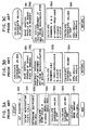
- Fig. 1 is a block diagram of a lead-bend measuring apparatus which shows a conventional example.
- the lead-bend measuring apparatus of this type conventionally comprises an inspection stage 38 on which an IC 2 is placed with its rear surface facing up by means of clamp claws 3a, 3b and 3c; a pair of annular incandescent lamps 4a for projecting light onto distal ends, proximal ends, and apex portions of the leads of the IC 2 as well as a pair of optical fiber arrays 4b connected to an incandescent lamp-house; a pair of camera heads 1, a camera driver 10, and a camera controller 11 for fetching the light reflected from and transmitted through the leads and for imaging the distal ends, proximal ends, and apex portions of the leads; an A/D converter 13 for fetching image signals from the camera controller 11 by means of a fetch clock 12 and converting the same into 256 gradations; a frame memory 15 for storing the image data converted into 256 gradations; a
- the CPU 23 comprises an area cutout unit 16 for fetching the image data of the entire imaged regions of the leads of the IC 2 from the frame memory 15 via I/O ports 14b, and for dividing the fetched image data into a plurality of divided regions designated by area-designating-pointer storage units 19a; a binarization processing unit 17 for binarizing the image data of the entire divided sections at a binarization level stored in advance in a binarization-level storage unit 20a, and for storing the binarised data in the binary image memory 18 connected to an external device via I/O ports 14d; a profile counter 21 for fetching the binarized data from the binary image memory 18 via I/O ports 14e and preparing an image profile of the leads; an area center-of-gravity calculating unit 22 for calculating the center of gravity of an area of the prepared profile; a lead-bend-amount calculating unit 25 for calculating a deviation of the center of gravity of the area from a reference profile position so as to obtain an amount of bend; and a
- the IC 2 is fed from the feeding section 6 to the inspection stage 38, and the IC 2 is placed on the inspection stage 38 with its rear surface facing up.
- the IC 2 is then fixed to the inspection stage 38 by means of the clamp claws 3a, 3b and 3c.
- light is projected onto the distal ends, proximal ends, and apex portions of the leads by means of the annular incandescent lamps 4a and the optical fiber arrays 4b.
- the camera heads 1 fetch the light reflected from or transmitted through the various portions of the leads and effect imaging.
- the camera controller 11 fetches imaging signals by means of the fetch clock 12, and the imaging signals are divided into 256 gradations by the A/D converter 13 and are stored in the frame memory 15.
- the area cutout unit 16 then divides all the image data of the frame memory 15 into a plurality of designated sections stored in advance in the area-designating-pointer storage units 19a.
- the binarization processing unit 17 effects binarization processing of all the image data of the areas divided by using one binarization level which is set in advance in the binarization-level storage unit 20a.
- the image data subjected to binarization processing is temporarily stored in the binary image memory 18.
- the profile counter 21 fetches the image data from the binary image memory 18 through the I/O ports 14e and prepares profiles of various portions of the leads.
- FIG. 2 is a diagram illustrating an algorithm for calculating an amount of bend in the lead-bend measuring apparatus shown in Fig. 1.
- Figs. 3A to 3C are flow-charts illustrating the algorithm. If it is assumed that the profile of each portion is depicted as shown in Fig. 2, in Step 310 of Fig. 3A, WINDOWs 1 and 2 shown in Fig. 2 are set by the area center-of-gravity calculating unit 22 and the lead-bend-amount calculating unit 25.
- Step 320 points a, b, c and d at which defining lines of the WINDOWs 1 and 2 and contour lines of the profile intersect each other are determined in Step 320.
- Step 330 mid-points between the respective pairs of points of intersection are determined and set as WG1 and WG2.
- Step 340 an angle ⁇ of inclination of the profile, i.e., an angle of bend, is determined from X-Y coordinate values of WG1 and WG2.
- Step 350 coordinates of a mid-point STP at one end of the profile are determined.
- the coordinates of STP are calculated as shown in Fig. 3B. Namely, in Step 351 of Fig.
- Step 352 a segment is extended from WG1 in parallel with the Y-axis. Then, in Step 352, the length of a segment A between the point WG1 and a point WG1VP is calculated. A segment B is determined from the segment A in Step 353. Then, the coordinates of STP are calculated in Step 354.
- Step 360 of Fig. 3A coordinate values of a mid-point SBP at the other end of the profile are determined in a similar manner in accordance with the flow-chart shown in Fig. 3C.
- Step 370 of Fig. 3A the difference between the X-axis components of the mid-points STP and SBP is calculated as the amount of bend.
- the non-defective/defective determining unit 24 allowable values of bend stored in advance in the external storage unit 26 are extracted, and a comparison is made between the same and the calculated amount of bend so as to determine the non-defective or defective state. Then, the horizontal transport mechanism section 5 is actuated by the sequencer 9, and the IC 2 whose non-defective or detective state has been determined is stored in the non-defective storage section 7 or the defective storage section 8. The inspection of the bend of IC leads has hitherto been effected automatically in the above-described manner.
- Figs. 4A to 4F are diagrams for explaining the problems in the conventional lead-bend measuring apparatus, in which Figs. 4A to 4D are graphs illustrating the distribution of illuminance at gradations, and Figs. 4E and 4F are diagrams illustrating the positions of sections in the leads.
- Figs. 4E and 4F are diagrams for explaining the problems in the conventional lead-bend measuring apparatus, in which Figs. 4A to 4D are graphs illustrating the distribution of illuminance at gradations, and Figs. 4E and 4F are diagrams illustrating the positions of sections in the leads.
- leads 39 are illuminated with light at sections 35a, 35b, 35c and 35d
- the distribution of illuminance differs for each of these sections, as shown in Figs. 9A to 9D.
- the sections 35a and 35b are imaged by one camera
- the sections 35c and 35d are imaged by another.
- an object of the present invention to provide a lead-bend measuring apparatus capable of effecting accurate measurement by making improvements on the binarization processing of a plurality of divided lead portions.
- a lead-bend measuring apparatus comprising: an illuminating means for projecting light onto leads projecting from a package of an integrated circuit device; an imaging means for imaging light reflected from and transmitted through the leads; a cutout means for fetching an image of the imaged light and dividing the image into a plurality of sections; a binarization processing means for processing gradations of the image with different binarization levels for each of the divided sections; a profile counter means for preparing profiles of various portions of the leads corresponding to the respective sections from binarized data subjected to processing by the binarization processing means; a calculating means for calculating a deviation of each of the prepared profiles from a reference profile and determining an amount of bend of each of the leads; and a means for determining a non-defective or defective state by making a comparison between the amount of bent calculated and allowable values.
- Fig. 5 is a block diagram of a lead-bend measuring apparatus in accordance with an embodiment of the present invention
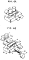
- Figs. 6A and 6B are enlarged perspective views of an inspection stage of the lead-bend measuring apparatus shown in Fig. 5
- Fig. 7 is a perspective view of a lower illuminating means for illuminating lead portions in the lead-bend measuring apparatus shown in Fig. 5.
- this lead-bend measuring apparatus is provided with binarization-level storage units 20b for storing the same number of binarization levels as the number of sections divided by an area cutout unit 16, as shown in Fig. 5.
- the lead-bend measuring apparatus of the present invention provided with the binarization-level storage units 20b is characterized in that clearer profiles of lead portions can be obtained as the binarization level selected for the dark and bright spots is changed in correspondence with the distribution of illuminance of light reflected from these sections.
- an IC 2 in Fig. 5 is gripped by a suction chuck of a horizontal transport mechanism section 5 which is controlled by a sequencer 9.
- the IC 2 is then moved horizontally and is transported from a feeding section 6 to an inspection stage 38.
- the IC 2 is placed on the inspection stage 38 with its rear surface facing upward, and is sucked with a vacuum so as to effect pre-alignment.
- the IC 2 is then fixed by means of a plurality of clamp claws 3a, 3b, 3c and 3d.
- the inspection stage 38 arranged in the state shown in Fig.
- the IC 2B is fed by a ball screw 30, and the IC 2 is positioned below a pair of annular incandescent lamps 4a, as shown in Fig. 6A. Then, the distal ends of the leads of the IC 2 and flat apex portions at their tops are irradiated by the annular incandescent lamps 4a, while the proximal ends of the leads are irradiated by a pair of optical fiber arrays 4b each comprised of optical fibers 4c and connected to an incandescent lamp-house 4d, as shown in Fig. 7.
- a pair of camera heads 1, a camera driver 10, and a camera controller 11 image the reflected images obtained thereby, and a fetch clock 12 and an 8-bit A/D converter 13 write the images to a frame memory 15 via I/O ports 14a with 256 gradations.
- a fetch clock 12 and an 8-bit A/D converter 13 write the images to a frame memory 15 via I/O ports 14a with 256 gradations.
- the area cutout unit 16 extracts a plurality of sections designated by area-designating-pointer storage units 19b, and divides the multivalued image data in the frame memory 15 into a plurality of sections.
- a binarization processing unit 17 fetches respective binarization levels corresponding to the sections from the binarization-level storage units 20b and effects binarization processing of the respective sections.
- the image data subjected to binarization processing is written to a binary image memory 18 via I/O ports 14d.
- an amount of bend of each lead is determined by a profile counter 21, an area-center-of-gravity calculating unit 22, and a lead-bend-amount calculating unit 25 by using the same algorithm as the one described for the prior art.
- the amount of bend of each lead thus calculated is compared with allowable values by a non-defective/defective determining unit 24 so as to determine the non-defective or defective state of the IC 2.
- Fig. 8 is a block diagram of the lead-bend measuring apparatus in accordance with another embodiment of the present invention.
- Fig. 9 is a perspective view of the inspection stage shown in Fig. 8 and an IC transport mechanism.
- a chute rail mechanism in which ICs are allowed to slide and drop by its own weight is adopted instead of the horizontal transport mechanism section which is used in the foregoing embodiment and in which each IC is gripped by a chuck and is moved. Namely, as shown in Fig.
- this IC transport mechanism comprises a chute rail 33a having a groove along which the package of the IC slides from the feeding section 6 onto the inspection stage 38; a positioning rail 33 having a vertically movable positioning stopper 34 at one end side thereof, the positioning rail 33 being secured on the inspection stage; and a pusher 33b for allowing the IC 2 discharged onto a placing table 33c from the positioning rail 33 to be dropped into a non-defective storage section 7 or a defective storage section 8 after completion of the inspection.
- the illuminating means of this lead-bend measuring apparatus is arranged such that a pair of rod-like parallel light sources 4e are arranged above the IC 2 and in parallel with the direction in which the leads are arrayed, and a reflecting mirror 32 for reflecting the light from the rod-like parallel light sources 4e is disposed substantially in the center of the IC 2 so as to illuminate the apex portions of the leads projecting from both sides of the IC 2 with this reflected light. Accordingly, the apex portions of the leads are imaged as transmitted images, and the distal ends as reflected images. In addition, the proximal ends of the leads are illuminated by the optical fiber arrays 4b in the same way as in the foregoing embodiment, and are imaged as reflected images.
- the IC 2 is first fed from the feeding section 6 to the chute rail 33a, the IC 2 slides along the chute rail 33a and drops onto the positioning rail 33.
- a sensor (not shown) is operated, and the stopper 34 is raised to position the IC 2.
- the IC 2 is then fixed by means of the clamp claws 3b and 3d.
- the camera heads 1, the camera driver 10, and the camera controller 11 pick up images, and the fetch clock 12 and the 8-bit A/D converter 13 write the images to the frame memory 15 with 256 gradations via the I/O ports 14a.
- the area cutout unit 16 cuts out the multivalued images into a plurality of sections designated by the area-designating-pointer storage units 19b.
- the binarization processing unit 17 then binarizes the cutout sections by using the binarization levels that are designated by the binarization-level storage units 20b on a one-to-one correspondence basis with respect to each section, and writes binarized image data to the binary image memory 18 through the I/O ports 14d.
- which portions of the images stored in the frame memory 15 are to be cut out is automatically transferred from an external storage unit 26 to the area-designating-pointer storage units 19b and is stored therein at the start of the apparatus.
- an operator of the apparatus is capable of newly preparing or revising these area-designating-pointer storage units 19b freely by operating a keyboard 27.
- the profile counter 21, the area-center-of-gravity calculating unit 22, and the lead-bend-amount calculating unit 25 calculate the amounts of bend of all the leads of the IC 2 on the basis of the binarized images which have been read through I/O ports 14e in accordance with the lead-bend calculating algorithm.
- the non-defective/defective determining unit 24 determines the non-defective or defective state by making a comparison with allowable values.
- the IC 2 for which the determination has been completed is discharged onto the placing table 33c from the positioning rail 33, and is transported to the non-defective storage section 7 or the defective storage section 7 by the pusher 33b.
- the apex portions of the leads are imaged as transmitted images, i.e., since images of the apex portions are stored in the binary image memory 18 as dark spots, the dark spots are converted to bright spots via an inverter 36 before they are fetched or loaded to the profile counter 21.
- the other portions of the leads i.e., the distal and proximal ends of the leads, are recorded in the binary image memory 18 as reflected images, i.e., bright spots, so that the image data thereof are processed as they are by the profile counter 21.
- a software switch 37 of a CPU 23 manages both an input line with the inverter 36 and a line without the same, and performs switching in such a manner as to effect inverted inputting with respect to the processing of the apex portions of the leads and non-inverted inputting with respect to the distal and proximal ends of the leads.
- the means for dividing the images of the leads into a plurality of sections and the means for setting binarization levels respectively corresponding to the divided sections and processing the sections with the corresponding binarization levels. Accordingly, there is an advantage in that even if the illuminance of the various portions of the leads is not uniform, it is possible to obtain clearer binarized images, thereby making it possible to effect measurements more accurately.
Abstract
Description
- The present invention relates to a lead-bend measuring apparatus for measuring an amount of bend of leads projecting from a package of an integrated circuit device (hereafter simply referred to as an "IC") so as to determine the non-defective or defective state of the product by comparing the measured results with allowable values.
- Fig. 1 is a block diagram of a lead-bend measuring apparatus which shows a conventional example. As shown in the drawings, the lead-bend measuring apparatus of this type conventionally comprises an
inspection stage 38 on which anIC 2 is placed with its rear surface facing up by means ofclamp claws incandescent lamps 4a for projecting light onto distal ends, proximal ends, and apex portions of the leads of theIC 2 as well as a pair ofoptical fiber arrays 4b connected to an incandescent lamp-house; a pair ofcamera heads 1, acamera driver 10, and a camera controller 11 for fetching the light reflected from and transmitted through the leads and for imaging the distal ends, proximal ends, and apex portions of the leads; an A/D converter 13 for fetching image signals from the camera controller 11 by means of afetch clock 12 and converting the same into 256 gradations; aframe memory 15 for storing the image data converted into 256 gradations; aCPU 23 adapted to fetch the image data from theframe memory 15, divide the fetched image data into a plurality of sections, binarize the image data of the divided sections, prepare a profile of various lead portions by means of this binarized data and calculate a deviation of that profile from a reference profile to determine an amount of bend of each lead, and compare this amount of bend with allowable values so as to determine the non-defective or defective state; aprinter 29, aCRT 28, akeyboard 27, and anexternal storage device 26 for storing the allowable values and the like, all of these units being connected to theCPU 23 via I/O ports 14f; abinary image memory 18 for temporarily storing the image data subjected to binarization processing by theCPU 23; afeeding section 6 for feedingICs 2; a horizontaltransport mechanism section 5 for transporting the ICs to anon-defective storing section 7 or adefective storing section 8 after the non-defective or defective state of the ICs is determined by theCPU 23; and asequencer 9 for controlling the various units. - The
CPU 23 comprises anarea cutout unit 16 for fetching the image data of the entire imaged regions of the leads of theIC 2 from theframe memory 15 via I/O ports 14b, and for dividing the fetched image data into a plurality of divided regions designated by area-designating-pointer storage units 19a; abinarization processing unit 17 for binarizing the image data of the entire divided sections at a binarization level stored in advance in a binarization-level storage unit 20a, and for storing the binarised data in thebinary image memory 18 connected to an external device via I/O ports 14d; aprofile counter 21 for fetching the binarized data from thebinary image memory 18 via I/O ports 14e and preparing an image profile of the leads; an area center-of-gravity calculating unit 22 for calculating the center of gravity of an area of the prepared profile; a lead-bend-amount calculating unit 25 for calculating a deviation of the center of gravity of the area from a reference profile position so as to obtain an amount of bend; and a non-defective/defective determiningunit 24 for determining the non-defective or detective state by comparing this amount of bend and allowable values stored in advance. - Next, a description will be given of the operation of this lead-bend measuring apparatus. First, the
IC 2 is fed from thefeeding section 6 to theinspection stage 38, and theIC 2 is placed on theinspection stage 38 with its rear surface facing up. TheIC 2 is then fixed to theinspection stage 38 by means of theclamp claws incandescent lamps 4a and theoptical fiber arrays 4b. Thecamera heads 1 fetch the light reflected from or transmitted through the various portions of the leads and effect imaging. The camera controller 11 fetches imaging signals by means of thefetch clock 12, and the imaging signals are divided into 256 gradations by the A/D converter 13 and are stored in theframe memory 15. Thearea cutout unit 16 then divides all the image data of theframe memory 15 into a plurality of designated sections stored in advance in the area-designating-pointer storage units 19a. Subsequently, thebinarization processing unit 17 effects binarization processing of all the image data of the areas divided by using one binarization level which is set in advance in the binarization-level storage unit 20a. The image data subjected to binarization processing is temporarily stored in thebinary image memory 18. Theprofile counter 21 fetches the image data from thebinary image memory 18 through the I/O ports 14e and prepares profiles of various portions of the leads. - A description will now be given of a method of calculating an amount of bend of each lead from the profiles of the various portions of the leads. Fig. 2 is a diagram illustrating an algorithm for calculating an amount of bend in the lead-bend measuring apparatus shown in Fig. 1. Figs. 3A to 3C are flow-charts illustrating the algorithm. If it is assumed that the profile of each portion is depicted as shown in Fig. 2, in
Step 310 of Fig. 3A, WINDOWs 1 and 2 shown in Fig. 2 are set by the area center-of-gravity calculating unit 22 and the lead-bend-amount calculating unit 25. Then, points a, b, c and d at which defining lines of theWINDOWs Step 320. InStep 330, mid-points between the respective pairs of points of intersection are determined and set as WG1 and WG2. InStep 340, an angle ϑ of inclination of the profile, i.e., an angle of bend, is determined from X-Y coordinate values of WG1 and WG2. InStep 350, coordinates of a mid-point STP at one end of the profile are determined. Here, the coordinates of STP are calculated as shown in Fig. 3B. Namely, inStep 351 of Fig. 3B, a segment is extended from WG1 in parallel with the Y-axis. Then, inStep 352, the length of a segment A between the point WG1 and a point WG1VP is calculated. A segment B is determined from the segment A inStep 353. Then, the coordinates of STP are calculated inStep 354. - Subsequently, in
Step 360 of Fig. 3A, coordinate values of a mid-point SBP at the other end of the profile are determined in a similar manner in accordance with the flow-chart shown in Fig. 3C. Then, inStep 370 of Fig. 3A, the difference between the X-axis components of the mid-points STP and SBP is calculated as the amount of bend. - Next, in the non-defective/defective determining
unit 24, allowable values of bend stored in advance in theexternal storage unit 26 are extracted, and a comparison is made between the same and the calculated amount of bend so as to determine the non-defective or defective state. Then, the horizontaltransport mechanism section 5 is actuated by thesequencer 9, and theIC 2 whose non-defective or detective state has been determined is stored in thenon-defective storage section 7 or thedefective storage section 8. The inspection of the bend of IC leads has hitherto been effected automatically in the above-described manner. - However, since the lead of the IC is complicate in shape, and the finished state of the surfaces of the leads is not necessarily uniform, it is impossible to obtain uniform intensity of light reflected from the various portions of the leads. As a result, the visibility of the projected images of various portions of the leads differs for each section, which in turn results in measurement errors, making it difficult to effect accurate measurement.
- Figs. 4A to 4F are diagrams for explaining the problems in the conventional lead-bend measuring apparatus, in which Figs. 4A to 4D are graphs illustrating the distribution of illuminance at gradations, and Figs. 4E and 4F are diagrams illustrating the positions of sections in the leads. A description will now be given of the aforementioned problems with reference to the drawings. For instance, as shown in Figs. 4E and 4F, if
leads 39 are illuminated with light atsections sections sections sections gradation 128 in the binarization processing level serving as a boundary, so that images of the same illuminance are obtained when the image data is processed at the same binarization level. However, in a case where the distribution of illuminance utterly differs in thesections - It is, therefore, an object of the present invention to provide a lead-bend measuring apparatus capable of effecting accurate measurement by making improvements on the binarization processing of a plurality of divided lead portions.
- To this end, in accordance with the present invention, there is provided a lead-bend measuring apparatus comprising:
an illuminating means for projecting light onto leads projecting from a package of an integrated circuit device;
an imaging means for imaging light reflected from and transmitted through the leads;
a cutout means for fetching an image of the imaged light and dividing the image into a plurality of sections;
a binarization processing means for processing gradations of the image with different binarization levels for each of the divided sections;
a profile counter means for preparing profiles of various portions of the leads corresponding to the respective sections from binarized data subjected to processing by the binarization processing means;
a calculating means for calculating a deviation of each of the prepared profiles from a reference profile and determining an amount of bend of each of the leads; and
a means for determining a non-defective or defective state by making a comparison between the amount of bent calculated and allowable values. - The above and other objects, features and advantages of the present invention will become more apparent from the following description of the invention when read in conjunction with the accompanying drawings, in which:
- Fig. 1 is a block diagram of a prior art example of the lead-bend measuring apparatus;
- Fig. 2 is a diagram illustrating an algorithm for calculating an amount of bend in the lead-bend measuring apparatus shown in Fig. 1;
- Figs. 3A to 3C are flow-charts illustrating the algorithm;
- Figs. 4A to 4F are diagrams for explaining the problem of the prior art lead-bend measuring apparatus, in which Figs. 4A to 4D are graphs illustrating the distribution of illuminance at gradations, while Figs. 4E to 4F are diagrams illustrating the positions of sections in the leads;
- Fig. 5 is a block diagram of a lead-bend measuring apparatus in accordance with an embodiment of the present invention;
- Figs. 6A and 6B are enlarged perspective views of an inspection stage of the lead-bend measuring apparatus shown in Fig. 5;
- Fig. 7 is a perspective view of a lower illuminating means for illuminating lead portions in the lead-bend measuring apparatus shown in Fig. 5;
- Fig. 8 is a block diagram of the lead-bend measuring apparatus in accordance with another embodiment of the present invention; and
- Fig. 9 is a perspective view of the inspection stage shown in Fig. 8 and an IC transport mechanism.
- Now, preferred embodiments according to the invention are explained with reference to the accompanying drawings. It is to be noted that, throughout the following explanation, the same or similar numerals refer to the same or like elements in all the figures of the drawings.
- Fig. 5 is a block diagram of a lead-bend measuring apparatus in accordance with an embodiment of the present invention; Figs. 6A and 6B are enlarged perspective views of an inspection stage of the lead-bend measuring apparatus shown in Fig. 5; and Fig. 7 is a perspective view of a lower illuminating means for illuminating lead portions in the lead-bend measuring apparatus shown in Fig. 5.
- It should be noted that this lead-bend measuring apparatus is provided with binarization-
level storage units 20b for storing the same number of binarization levels as the number of sections divided by anarea cutout unit 16, as shown in Fig. 5. The lead-bend measuring apparatus of the present invention provided with the binarization-level storage units 20b is characterized in that clearer profiles of lead portions can be obtained as the binarization level selected for the dark and bright spots is changed in correspondence with the distribution of illuminance of light reflected from these sections. - A description will now be given of the operation of this lead-bend measuring apparatus. First, an
IC 2 in Fig. 5 is gripped by a suction chuck of a horizontaltransport mechanism section 5 which is controlled by asequencer 9. TheIC 2 is then moved horizontally and is transported from afeeding section 6 to aninspection stage 38. Then, as shown in Fig. 6, theIC 2 is placed on theinspection stage 38 with its rear surface facing upward, and is sucked with a vacuum so as to effect pre-alignment. TheIC 2 is then fixed by means of a plurality ofclamp claws inspection stage 38 arranged in the state shown in Fig. 2B is fed by aball screw 30, and theIC 2 is positioned below a pair of annularincandescent lamps 4a, as shown in Fig. 6A. Then, the distal ends of the leads of theIC 2 and flat apex portions at their tops are irradiated by the annularincandescent lamps 4a, while the proximal ends of the leads are irradiated by a pair ofoptical fiber arrays 4b each comprised ofoptical fibers 4c and connected to an incandescent lamp-house 4d, as shown in Fig. 7. - Subsequently, as shown in Fig. 5, a pair of camera heads 1, a
camera driver 10, and a camera controller 11 image the reflected images obtained thereby, and a fetchclock 12 and an 8-bit A/D converter 13 write the images to aframe memory 15 via I/O ports 14a with 256 gradations. It should be noted that all of the distal ends, flat apex portions at the tops, and the proximal ends of the leads are imaged as reflected images. Then, thearea cutout unit 16 extracts a plurality of sections designated by area-designating-pointer storage units 19b, and divides the multivalued image data in theframe memory 15 into a plurality of sections. Abinarization processing unit 17 fetches respective binarization levels corresponding to the sections from the binarization-level storage units 20b and effects binarization processing of the respective sections. The image data subjected to binarization processing is written to abinary image memory 18 via I/O ports 14d. Subsequently, an amount of bend of each lead is determined by aprofile counter 21, an area-center-of-gravity calculating unit 22, and a lead-bend-amount calculating unit 25 by using the same algorithm as the one described for the prior art. The amount of bend of each lead thus calculated is compared with allowable values by a non-defective/defective determiningunit 24 so as to determine the non-defective or defective state of theIC 2. - Fig. 8 is a block diagram of the lead-bend measuring apparatus in accordance with another embodiment of the present invention. Fig. 9 is a perspective view of the inspection stage shown in Fig. 8 and an IC transport mechanism. In this lead-bend measuring apparatus, a chute rail mechanism in which ICs are allowed to slide and drop by its own weight is adopted instead of the horizontal transport mechanism section which is used in the foregoing embodiment and in which each IC is gripped by a chuck and is moved. Namely, as shown in Fig. 9, this IC transport mechanism comprises a
chute rail 33a having a groove along which the package of the IC slides from thefeeding section 6 onto theinspection stage 38; apositioning rail 33 having a verticallymovable positioning stopper 34 at one end side thereof, thepositioning rail 33 being secured on the inspection stage; and apusher 33b for allowing theIC 2 discharged onto a placing table 33c from thepositioning rail 33 to be dropped into anon-defective storage section 7 or adefective storage section 8 after completion of the inspection. - As shown in Fig. 9, the illuminating means of this lead-bend measuring apparatus is arranged such that a pair of rod-like parallel
light sources 4e are arranged above theIC 2 and in parallel with the direction in which the leads are arrayed, and a reflectingmirror 32 for reflecting the light from the rod-like parallellight sources 4e is disposed substantially in the center of theIC 2 so as to illuminate the apex portions of the leads projecting from both sides of theIC 2 with this reflected light. Accordingly, the apex portions of the leads are imaged as transmitted images, and the distal ends as reflected images. In addition, the proximal ends of the leads are illuminated by theoptical fiber arrays 4b in the same way as in the foregoing embodiment, and are imaged as reflected images. - In the operation of this lead-bend measuring apparatus, the
IC 2 is first fed from thefeeding section 6 to thechute rail 33a, theIC 2 slides along thechute rail 33a and drops onto thepositioning rail 33. As a result, a sensor (not shown) is operated, and thestopper 34 is raised to position theIC 2. TheIC 2 is then fixed by means of theclamp claws camera driver 10, and the camera controller 11 pick up images, and the fetchclock 12 and the 8-bit A/D converter 13 write the images to theframe memory 15 with 256 gradations via the I/O ports 14a. Then, thearea cutout unit 16 cuts out the multivalued images into a plurality of sections designated by the area-designating-pointer storage units 19b. Thebinarization processing unit 17 then binarizes the cutout sections by using the binarization levels that are designated by the binarization-level storage units 20b on a one-to-one correspondence basis with respect to each section, and writes binarized image data to thebinary image memory 18 through the I/O ports 14d. Here, which portions of the images stored in theframe memory 15 are to be cut out is automatically transferred from anexternal storage unit 26 to the area-designating-pointer storage units 19b and is stored therein at the start of the apparatus. In addition, an operator of the apparatus is capable of newly preparing or revising these area-designating-pointer storage units 19b freely by operating akeyboard 27. - Returning to the description of the operation, the
profile counter 21, the area-center-of-gravity calculating unit 22, and the lead-bend-amount calculating unit 25 calculate the amounts of bend of all the leads of theIC 2 on the basis of the binarized images which have been read through I/O ports 14e in accordance with the lead-bend calculating algorithm. The non-defective/defective determiningunit 24 determines the non-defective or defective state by making a comparison with allowable values. TheIC 2 for which the determination has been completed is discharged onto the placing table 33c from thepositioning rail 33, and is transported to thenon-defective storage section 7 or thedefective storage section 7 by thepusher 33b. - Since the apex portions of the leads are imaged as transmitted images, i.e., since images of the apex portions are stored in the
binary image memory 18 as dark spots, the dark spots are converted to bright spots via aninverter 36 before they are fetched or loaded to theprofile counter 21. The other portions of the leads, i.e., the distal and proximal ends of the leads, are recorded in thebinary image memory 18 as reflected images, i.e., bright spots, so that the image data thereof are processed as they are by theprofile counter 21. Asoftware switch 37 of aCPU 23 manages both an input line with theinverter 36 and a line without the same, and performs switching in such a manner as to effect inverted inputting with respect to the processing of the apex portions of the leads and non-inverted inputting with respect to the distal and proximal ends of the leads. - In this embodiment, since images of the apex portions of the leads are fetched as transmitted images, the apex portions of the leads can be imaged more clearly as compared with the earlier explained embodiment in which images of the apex portions are fetched as reflected images. Hence, there is an advantage in that measurements can be effected with higher accuracy. In addition, there is an advantage in that the IC mechanism for transporting the
ICs 2 is inexpensive. Furthermore, there is another advantage in that, since rod-like parallel light sources disposed in parallel with the direction in which the leads are arrayed are used as the illuminating means, the illuminance for the leads can be made more uniform. - As described above, in accordance with the present invention, there are provided the means for dividing the images of the leads into a plurality of sections and the means for setting binarization levels respectively corresponding to the divided sections and processing the sections with the corresponding binarization levels. Accordingly, there is an advantage in that even if the illuminance of the various portions of the leads is not uniform, it is possible to obtain clearer binarized images, thereby making it possible to effect measurements more accurately.
- While the invention has been described in its preferred embodiments, it is to be understood that the words which have been used are words of description rather than limitation and that changes within the purview of the appended claims may be made without departing from the true scope and spirit of the invention in its broader aspects.
Claims (9)
- A lead-bend measuring apparatus characterized by comprising:
an illuminating means (4a, 4b, 4c, 4d, 4e) for projecting light onto leads projecting from a package of an integrated circuit device (2);
an imaging means (1, 10, 11) for imaging light reflected from and transmitted through the leads;
a cutout means (16, 19b) for fetching an image of the imaged light and dividing the image into a plurality of sections;
a binarization processing means (17, 20b) for processing gradations of the image with different binarization levels for each of the divided sections;
a profile counter means (21) for preparing profiles of various portions of the leads corresponding to the respective sections from binarized data subjected to processing by said binarization processing means;
a calculating means (22, 25) for calculating a deviation of each of the prepared profiles from a reference profile and determining an amount of bend of each of the leads; and
a means (24) for determining a non-defective or defective state by making a comparison between the amount of bent calculated and allowable values. - A lead-bend measuring apparatus according to claim 1, wherein said illuminating means includes a pair of annular incandescent lamps (4a) for illuminating distal ends and apex portions of the leads and a pair of optical fiber arrays (4b) for illuminating proximal ends of the leads.
- A lead-bend measuring apparatus according to claim 1, wherein said illuminating means includes a pair of rod-like parallel light sources (4e) arranged in parallel with the direction in which the leads are arrayed, and a reflecting mirror (32) disposed substantially in the center of the integrated circuit device for reflecting the light from the rod-like parallel light sources so as to illuminate the apex portions of the leads projecting from both sides of the integrated circuit device.
- A lead-bend measuring apparatus according to claim 1, wherein said imaging means includes a pair of camera heads (1), a camera driver (10), and a camera controller (11) for fetching the light reflected from and transmitted through the leads and for imaging the distal ends, proximal ends, and apex portions of the leads.
- A lead-bend measuring apparatus according to claim 1, wherein said cutout means (16, 19b) includes an area cutout unit (16) for cutting out the image into the plurality of sections and area-designating-pointer storage units (19b) for designating the sections to be cut out by said area cutout unit (16).
- A lead-bend measuring apparatus according to claim 1, wherein said binarization processing means (17, 20b) includes a binarization processing unit (17) for fetching binarization levels corresponding to the cutout sections and effecting binarization processing of the cutout sections and binarization-level storage units (20b) for storing the same number of binarization levels as the number of sections divided by said cutout means.
- A lead-bend measuring apparatus according to claim 1, further comprising a transport mechanism (5, 33a, 33, 33b, 34) for transporting the integrated circuit device to a non-defective storing section (7) or a defective storing section (8) after the non-defective or defective state of the integrated circuit device is determined.
- A lead-bend measuring apparatus according to claim 7, wherein said transport mechanism is a horizontal transport mechanism in which the integrated circuit device (2) is gripped by a chuck and is moved thereby.
- A lead-bend measuring apparatus according to claim 7, wherein said transport mechanism includes a chute rail (33a) having a groove along which the package of the integrated circuit device (2) slides from a feeding section (6) onto an inspection stage (38), a positioning rail (33) having a vertically movable positioning stopper (34) at one end side thereof, and a pusher (33b) for allowing the integrated circuit device discharged onto a placing table (33c) from the positioning rail (33) to be dropped into the non-defective storage section (7) for storing non-defective integrated circuit devices or the defective storage section (8) for storing defective integrated circuit devices after completion of the measurement.
Applications Claiming Priority (2)
| Application Number | Priority Date | Filing Date | Title |
|---|---|---|---|
| JP29828/92 | 1992-02-18 | ||
| JP4029828A JPH06137839A (en) | 1992-02-18 | 1992-02-18 | Lead bending measuring device |
Publications (2)
| Publication Number | Publication Date |
|---|---|
| EP0560096A2 true EP0560096A2 (en) | 1993-09-15 |
| EP0560096A3 EP0560096A3 (en) | 1993-11-03 |
Family
ID=12286891
Family Applications (1)
| Application Number | Title | Priority Date | Filing Date |
|---|---|---|---|
| EP19930102569 Withdrawn EP0560096A3 (en) | 1992-02-18 | 1993-02-18 | Apparatus for measuring bend amount of ic leads |
Country Status (3)
| Country | Link |
|---|---|
| US (1) | US5412477A (en) |
| EP (1) | EP0560096A3 (en) |
| JP (1) | JPH06137839A (en) |
Cited By (4)
| Publication number | Priority date | Publication date | Assignee | Title |
|---|---|---|---|---|
| WO1994024700A1 (en) * | 1993-04-16 | 1994-10-27 | Modular Vision Systems Inc. | Qfp lead quality inspection system and method |
| EP0678911A2 (en) * | 1994-04-20 | 1995-10-25 | Siemens Aktiengesellschaft | System and method for inspecting semiconducter wafers |
| EP0678910A2 (en) * | 1994-04-20 | 1995-10-25 | Siemens Aktiengesellschaft | Inspection system for semiconductor wafers |
| WO1999005702A1 (en) * | 1997-07-23 | 1999-02-04 | Siemens Aktiengesellschaft | Testing and correction of faulty contact arrangements of integrated semiconductor components |
Families Citing this family (2)
| Publication number | Priority date | Publication date | Assignee | Title |
|---|---|---|---|---|
| JP3298753B2 (en) * | 1994-10-14 | 2002-07-08 | 株式会社新川 | Wire bending inspection device |
| US5877803A (en) * | 1997-04-07 | 1999-03-02 | Tritech Mircoelectronics International, Ltd. | 3-D image detector |
Citations (10)
| Publication number | Priority date | Publication date | Assignee | Title |
|---|---|---|---|---|
| JPS63181341A (en) * | 1987-01-23 | 1988-07-26 | Toshiba Corp | Apparatus and method for visual inspection of lead |
| JPS63265440A (en) * | 1987-04-22 | 1988-11-01 | Mitsubishi Electric Corp | Inspecting apparatus for lead shape of semiconductor device |
| JPH01233349A (en) * | 1988-03-14 | 1989-09-19 | Nec Corp | Lead bend detecting apparatus for semiconductor device |
| JPH01265144A (en) * | 1988-04-15 | 1989-10-23 | Sony Corp | Lead deformation checking method for packaging parts |
| JPH02136707A (en) * | 1988-11-16 | 1990-05-25 | Nec Corp | Lead bend detector |
| JPH03165536A (en) * | 1989-11-24 | 1991-07-17 | Nec Corp | Coplanarity measuring device |
| JPH03285341A (en) * | 1990-04-02 | 1991-12-16 | M B K Maikurotetsuku:Kk | Lead scanner |
| JPH0475359A (en) * | 1990-07-17 | 1992-03-10 | Nec Corp | Coplanarity measuring device |
| JPH0480937A (en) * | 1990-07-24 | 1992-03-13 | Nec Corp | Lead bending measuring device |
| JPH04102346A (en) * | 1990-08-22 | 1992-04-03 | Nec Corp | Lead-bend inspection apparatus of semiconductor device |
Family Cites Families (4)
| Publication number | Priority date | Publication date | Assignee | Title |
|---|---|---|---|---|
| US4995157A (en) * | 1989-05-16 | 1991-02-26 | Reel-Tech Inc. | Component feeder system |
| JPH083405B2 (en) * | 1989-06-30 | 1996-01-17 | 松下電器産業株式会社 | Lead position recognition device |
| EP0430860A3 (en) * | 1989-11-21 | 1993-01-13 | Toyo Ink Mfg. Co., Ltd. | Binarization processing method for multivalued image and method to form density pattern for reproducing binary gradations |
| US5168528A (en) * | 1990-08-20 | 1992-12-01 | Itt Corporation | Differential electronic imaging system |
-
1992
- 1992-02-18 JP JP4029828A patent/JPH06137839A/en active Pending
-
1993
- 1993-02-17 US US08/018,864 patent/US5412477A/en not_active Expired - Fee Related
- 1993-02-18 EP EP19930102569 patent/EP0560096A3/en not_active Withdrawn
Patent Citations (10)
| Publication number | Priority date | Publication date | Assignee | Title |
|---|---|---|---|---|
| JPS63181341A (en) * | 1987-01-23 | 1988-07-26 | Toshiba Corp | Apparatus and method for visual inspection of lead |
| JPS63265440A (en) * | 1987-04-22 | 1988-11-01 | Mitsubishi Electric Corp | Inspecting apparatus for lead shape of semiconductor device |
| JPH01233349A (en) * | 1988-03-14 | 1989-09-19 | Nec Corp | Lead bend detecting apparatus for semiconductor device |
| JPH01265144A (en) * | 1988-04-15 | 1989-10-23 | Sony Corp | Lead deformation checking method for packaging parts |
| JPH02136707A (en) * | 1988-11-16 | 1990-05-25 | Nec Corp | Lead bend detector |
| JPH03165536A (en) * | 1989-11-24 | 1991-07-17 | Nec Corp | Coplanarity measuring device |
| JPH03285341A (en) * | 1990-04-02 | 1991-12-16 | M B K Maikurotetsuku:Kk | Lead scanner |
| JPH0475359A (en) * | 1990-07-17 | 1992-03-10 | Nec Corp | Coplanarity measuring device |
| JPH0480937A (en) * | 1990-07-24 | 1992-03-13 | Nec Corp | Lead bending measuring device |
| JPH04102346A (en) * | 1990-08-22 | 1992-04-03 | Nec Corp | Lead-bend inspection apparatus of semiconductor device |
Non-Patent Citations (10)
| Title |
|---|
| PATENT ABSTRACTS OF JAPAN vol. 012, no. 457 (E-688) 30 November 1988 & JP 63 181341 A (TOSHIBA CORP) 26 July 1988 * |
| PATENT ABSTRACTS OF JAPAN vol. 013, no. 086 (E-720) 28 February 1989 & JP 63 265440 A (MITSUBISHI ELECTRIC CORP) 01 November 1988 * |
| PATENT ABSTRACTS OF JAPAN vol. 013, no. 557 (P-974) 12 December 1989 & JP 01 233349 A (NEC CORP) 19 September 1989 * |
| PATENT ABSTRACTS OF JAPAN vol. 014, no. 025 (P-991) 18 January 1990 & JP 01 265144 A (SONY CORP) 23 October 1989 * |
| PATENT ABSTRACTS OF JAPAN vol. 014, no. 369 (P-1090) 09 August 1990 & JP 02 136707 A (NEC CORP) 25 May 1990 * |
| PATENT ABSTRACTS OF JAPAN vol. 015, no. 405 (E-1122) 16 October 1991 & JP 03 165536 A (NEC CORP) 17 July 1991 * |
| PATENT ABSTRACTS OF JAPAN vol. 016, no. 116 (E-1181) 24 March 1992 & JP 03 285341 A (NEC CORP) 16 December 1991 * |
| PATENT ABSTRACTS OF JAPAN vol. 016, no. 291 (E-1224) 26 June 1992 & JP 04 075359 A (NEC CORP) 10 March 1992 * |
| PATENT ABSTRACTS OF JAPAN vol. 016, no. 300 (E-1227) 02 July 1992 & JP 04 080937 A (NEC CORP) 13 March 1992 * |
| PATENT ABSTRACTS OF JAPAN vol. 016, no. 340 (E-1238) 23 July 1992 & JP 04 102346 A (NEC CORP) 03 April 1992 * |
Cited By (6)
| Publication number | Priority date | Publication date | Assignee | Title |
|---|---|---|---|---|
| WO1994024700A1 (en) * | 1993-04-16 | 1994-10-27 | Modular Vision Systems Inc. | Qfp lead quality inspection system and method |
| EP0678911A2 (en) * | 1994-04-20 | 1995-10-25 | Siemens Aktiengesellschaft | System and method for inspecting semiconducter wafers |
| EP0678910A2 (en) * | 1994-04-20 | 1995-10-25 | Siemens Aktiengesellschaft | Inspection system for semiconductor wafers |
| EP0678911A3 (en) * | 1994-04-20 | 1996-04-17 | Siemens Ag | System and method for inspecting semiconducter wafers. |
| EP0678910A3 (en) * | 1994-04-20 | 1996-04-17 | Siemens Ag | Inspection system for semiconductor wafers. |
| WO1999005702A1 (en) * | 1997-07-23 | 1999-02-04 | Siemens Aktiengesellschaft | Testing and correction of faulty contact arrangements of integrated semiconductor components |
Also Published As
| Publication number | Publication date |
|---|---|
| JPH06137839A (en) | 1994-05-20 |
| US5412477A (en) | 1995-05-02 |
| EP0560096A3 (en) | 1993-11-03 |
Similar Documents
| Publication | Publication Date | Title |
|---|---|---|
| US4942618A (en) | Method and apparatus for determining the shape of wire or like article | |
| US6141040A (en) | Measurement and inspection of leads on integrated circuit packages | |
| US5495337A (en) | Method of visualizing minute particles | |
| US5621530A (en) | Apparatus and method for verifying the coplanarity of a ball grid array | |
| EP1557876A1 (en) | Probe mark reader and probe mark reading method | |
| JP2870142B2 (en) | Coplanarity measuring method and apparatus | |
| JP5421763B2 (en) | Inspection apparatus and inspection method | |
| EP0222072A2 (en) | Method of loading surface mounted device and an apparatus therefor | |
| JPH06103165B2 (en) | How to measure the height of circuit elements on a board | |
| JP2009156877A (en) | Three-dimensional inspection system | |
| JPH11351827A (en) | Image processor | |
| JP3311135B2 (en) | Inspection range recognition method | |
| CN101587084B (en) | Needle track inspection device, detecting device and needle track checking procedure | |
| JP3333615B2 (en) | Apparatus and method for measuring dimensions of semiconductor device | |
| US5058177A (en) | Method for inspection of protruding features | |
| US5412477A (en) | Apparatus for measuring bend amount of IC leads | |
| KR20000054979A (en) | Method for inspecting lead pins of IC package and apparatus therefor | |
| JP2000131037A (en) | Apparatus for inspecting shape of body | |
| JPH0429007A (en) | Optical inspection device | |
| JP3219094B2 (en) | Chip size detection method, chip pitch detection method, chip array data automatic creation method, and semiconductor substrate inspection method and apparatus using the same | |
| JPH07119705B2 (en) | Electronic component inspection device | |
| JP2003065754A (en) | Method and device for measuring flatness of semiconductor device package | |
| JP2946570B2 (en) | Coplanarity measuring device | |
| JP2569883B2 (en) | Coplanarity measuring device | |
| JP2000011173A (en) | Method for recognizing image and device therefor |
Legal Events
| Date | Code | Title | Description |
|---|---|---|---|
| PUAI | Public reference made under article 153(3) epc to a published international application that has entered the european phase |
Free format text: ORIGINAL CODE: 0009012 |
|
| AK | Designated contracting states |
Kind code of ref document: A2 Designated state(s): DE FR GB |
|
| PUAL | Search report despatched |
Free format text: ORIGINAL CODE: 0009013 |
|
| AK | Designated contracting states |
Kind code of ref document: A3 Designated state(s): DE FR GB |
|
| 17P | Request for examination filed |
Effective date: 19930927 |
|
| 17Q | First examination report despatched |
Effective date: 19950620 |
|
| STAA | Information on the status of an ep patent application or granted ep patent |
Free format text: STATUS: THE APPLICATION IS DEEMED TO BE WITHDRAWN |
|
| 18D | Application deemed to be withdrawn |
Effective date: 19960103 |